Note: Descriptions are shown in the official language in which they were submitted.
CA 02354018 2001-06-06
WO 00/36583 PCTIUS99/29673
PORTABLE MICRODISPLA.Y SYSTEM
RELATED APPLICATIONS
This application claims the benefit of U.S. Application No. 60/112,147 filed
on December 14, 1998 and U.S. Application No. 60V12I,899 filed on February 26,
1999, the entire contents of which are incorporated '.herein by reference.
BACKGROUND OF THE INVENTION
Flat-panel displays are being developed which utilize liquid crystals or
electroluminescent materials to produce high qualit;r images. These displays
are
expected to supplant cathode ray tube (CRT) technology and provide a
more highly defined television picture or computer monitor image. The most
promising mute to large scale high quality liquid cr~rstal displays (LCDs},
for
example, is the active-matrix approach in which thin-film transistors (TFTs)
are
co-located with LCD pixels. The primary advantagE; of the active matrix
approach
using TFTs is the elimination of cross-talk between pixels, and the excellent
gray
scale that can be attained with TFT-compatible LCDs.
CA 02354018 2001-06-06
- WO 00/36583 _ 2 _ PCT/US99I29b73
Color liquid crystal flat panel displays can be made in several different ways
including with color filters or sequentially flashing lights. Both style
displays are
found in transmissive or reflective models.
Transmissive color filter liquid crystal flat panel displays generally include
five different layers: a white light source, a first polarizing filter that is
mounted on
one side of a circuit panel on which the TFTs are arrayed to form pixels, a
filter plate
containing at least three primary colors arranged into pixels, and finally a
second
polarizing filter. A volume between the circuit panel and the filter plate is
filled with
a liquid crystal material. This material will allow transmission of light in
the
material when an electric field is applied across the rnateria,l between the
circuit
panel and a ground affixed to the filter plate. Thus, when a particular pixel
of the
display is turned on by the TFTs, the liquid crystal rr.~aterial rotates
polarized light
being transmitted through the material so that the light will pass through the
second
polarizing filter.
In sequential color displays, the display panel. is triple scanned, once for
each
primary color with the associated color light directed at the display panel.
For
example, to produce color frames at 20 Hz, the active; matrix must be driven
at a
frequency of 60 Hz. 1n order to reduce flicker, it is desirable to drive the
active
matrix at 180 Hz to produce a 60 Hz color image. At: over 60 Hz, visible
flicker is
reduced.
Owing to the limitations of amorphous silicor.~, other alternative materials
include polycrystalline silicon, or laser recrystallized silicon. These
materials are
limited as they use silicon that is akeady on glass, which generally restricts
further
circuit processing to low temperatures.
Tntegrated circuits for displays, such as the above-referred color sequential
display, are becoming more and more complex: For e;xampie, the color
sequential
display is designed for displaying High Definition Television (I~T'~ formats
requiring a 1280-by-1024 pixel array with a pixel pitch, or the distance
between lines
connecting adjacent columns or rows of pixel electrodes, being in the range of
15-55
microns, and fabricated on a single five-inch wafer.
CA 02354018 2001-06-06
- WO 00!36583 _ 3 _ PCT/US99I29693
SU1~IMARY OF THE INVENTION
This invention relates to a microdisplay and :more specifically to a small
area
high resolution liquid crystal display and methods for making such displays.
The
display has an array of at least 72,000 pixel electrodes and an active area of
less than
200 mm2, for example.
In a preferred method of displaying an image, an image is written to a liquid
crystal display having a plurality of pixel electrodes therein causing the
liquid crystal
to move to a specific image position. A light source is flashed to illuminate
the
display. The pixel electrodes are set to a specific electric field intensity
to cause the
liquid crystal to move towards a desired orientation or position before the
next image
is written. The process of writing, flashing and settiylg produces a desired
image.
In a preferred method, the image is a color image and the writing of the image
is associated with two or more color that are flashed after the writing steps
are
repeated for each of the plurality of colors. The voltage of the
counterelectrode is
switched after each flashing of the light source and prior to the next writing
of the
image. The liquid crystal display is an active matrix display having at least
75,000
pixel electrodes and having an active area of less tha'1 160 mm2.
In preferred embodiments, an active matrix color sequential liquid crystal
display has an active matrix circuit, a counterelectrode plane or layer, and
an
interposed layer of liquid crystal. The active matrix circuit has an array of
transistor
circuits formed in a first plane. Each transistor circuit is connected to a
pixel
electrode in an array of pixel electrodes having an area of 200 mm2 or less
and
preferably under 100 mm2. The counterelectrode panel extends in a second plane
that is parallel to the first plane and receives an applied voltage. The
liquid crystal
layer is interposed in a cavity between the two planes. The cavity has a depth
along
an axis perpendicular to the f rst and second planes o:f less than 3 microns.
in a preferred embodiment, an oxide layer extends between the pixel
electrode array and a layer of liquid crystal material. The oxide has a first
thickness
in a peripheral region around the array of pixel electrodes and a thinner
second
thickness in a pixel electrode region extending over tlae array of pixel
electrodes.
The thick peripheral region (about 0.5 microns in a preferred embodiment)
serves to
CA 02354018 2001-06-06
WO 00/36583 _ q, _ PCT/US99129673
better isolate the driver electrodes integrated into the display circuit. The
thinner
oxide region (about 0.3 microns) serves to reduce the voltage drop across the
oxide
during display operations. This serves to increase the applied voltage on the
liquid
crystal without the need to draw more power from the power source such as a
battery.
One preferred method of controlling the liquid crystal is to invert the input
video signal to eliminate DC voltage buildup on the liquid crystal material.
While
column inversion, where alternating columns receive video and inverted video,
is a
common mode, it is recognized that row, pixel or frune inversion can be
preferred in
some nodes. Another preferred method of controlling the liquid crystal in the
display
is to switch the voltage applied to the counterelectrode panel at the
beginning of the
subframe. In addition to eliminating non-symmetrical voltages, the technique
of
switching the voltage to the counterelectrode panel after every subframe
improves
contrast.
In addition to the switching of the voltage to the counterelectrode, there are
several other techniques that can be used in conjunction with or separately
from the
switching of the voltage to improve the quality of the image on the display.
It has
been recognized that the temperature of the microdisplay and in particular the
liquid
crystal effects the response of the liquid crystal and the brightness and the
color
uniformity of the image on the display.
An alternative method and one which can be used independently or in
conjunction with the switching of the voltage of the c;ounterelectrode is to
initialize
the pixels Vp~L to VcoM after flashing the backlight. With the pixel
electrodes set to
VIM, the liquid crystal begins to relax to the clear state, if the liquid
crystal
associated with the pixel was in some other state. Th.e liquid crystal
associated with
each pixel is relaxing, rotating to the clear state, until that pixel is
written to and
receives the signal or voltage associated with that image. In that the pixels
are
written in sequence, there is a greater time from writing until flashing the
light source
for the first pixels then the last pixels. The frst pixels will have the
majority of the
writing period to get to their desired position after receiving the video
signal and the
initializing of the pixel to VcoM will have minimum effect. However, the
pixels
CA 02354018 2001-06-06
WO 00136583 _ $ _ PCT/US99/29673
which receive their signal last and which have been initalized to clear and
have the
assocaited liquid crystal rotating towards clear if not: akeady there, will be
clear or
near clear prior to receiving their signal. The liquid crystal in this
preferred
embodiment is oriented such that it takes less time to drive black than relax
white.
Therefore, with the last pixels being at or near clear, the response time is
quicker
driving to black than if the pixels were black and relaxing to clear. The
initialization
of the display so that the liquid crystal is rotating towards the state which
takes
longest to reach, the clear state in a preferred embodiment, the individual
pixel
elements upon being set are closer to the settle positiion upon the flash of
the light
source.
The characteristics of the liquid crystal material are effected by the
temperature of the liquid crystal. For example, the twist time of twisted-
nematic
liquid crystal material is shorter when the liquid cry.ctal material is warm.
By
knowing the temperature of the liquid crystal, the duration and timing of the
flash of
the backlight can be set to achieve the desired brightness and minimizing
power
consumption.
The liquid crystal can be heated by several alternative embodiments. In one
preferred embodiment, the display is placed in a heat mode wherein multiple
rows
are turned on and a voltage drop occurs across the row Nines, creating heat.
The measuring of the temperature of the liquid crystal requires additional
analog circuitry which adds complexity to the circuit; of the display. It is
recognized
that it is the operational characteristics of the liquid <;rystal, not the
actual
temperature, that is ultimately desired. In one preferred embodiment, an
electrical
measurement of the liquid crystal capacitance is performed instead of the
measurement of temperature in order to determine when heating is required.
When
the heater is on and the duration that the heater is on does not need to be
based on the
temperature and can be actuated in response to a liquid crystal sensor that
responds to
optical, electrical or other property of the liquid crystal.
In one preferred embodiment, a sensor is incorporated to determine if the
liquid crystal is approaching the characteristic clearing temperature of the
liquid
crystal. The clearing temperature sensor is located just off the active
display area.
CA 02354018 2001-06-06
WO 00/36583 _ 6 _ PCT/US99/29673
The capacitance of a white (clear) pixel and a black pixel converge as the
liquid
crystal approaches its characteristic clearing temperature.
One of the traits of liquid crystal that is desired is the long time constant
which allows the image to be maintained without having to refresh in certain
instances. While a long time constant is generally a benefit, it can be a
detriment in
instances where the display is powered down and powered up a short time later.
Upon powering up the system, a portion of the previious image may remain.
In a preferred embodiment, an analog compa~rator samples the voltage of the
main power in real time. When the voltage drops below the level to run the
circuit
plus some margin, such as 90 percent, the display is powered down. In powering
down the display, a reset signal (PDR*) is asserted low. On receipt of the
PDR*
signal, the display circuitry will place VDD on all th.e column lines, and
activate ail
the row lines. The other end of the storage capacitor for each pixel is tied
to the
previous row line. This in effect discharges the storage capacitor to zero (0)
volts.
The normal timing continues for two or more cycles, therein sequentially
activating
alI the even and odd rows. This drives zero (0) volts on the column lines into
every
pixel.
Because the storage capacitor is several time:. larger than the pixel
capacitor,
the voltage on the storage capacitor will then discharge the pixel capacitor
to zero (0)
volts. At this point the display can be de-energized without any residual
charge left
on either the storage or pixel capacitor.
The increasing capability of microdisplays at the same time as the decrease in
size of the microdisplay has allowed for devices that were not possible prior
to the
invention of microdisplays or allow devices with increased capability. These
devices
included digital cameras, digital printers and improved camcorder viewfnders.
In a preferred embodiment, the microdisplay its used within a digital camera.
The microdisplay is used to both display the image to be taken and to display
images
stored within memory within the digital camera.
BRIEF DESCRIPTION OF THE DRAWINGS
CA 02354018 2001-06-06
WO 00/36583 - ~ - PCT/US99/29673
The above and other objects and features of the invention will be better
understood and appreciated by those skilled in the art in view of the
description of
the preferred embodiments given below in conjunction with the accompanying
drawings, in which:
FIG. 1 is a perspective view of a single wafer having a plurality of display
devices formed thereon in accordance with the invention;
FIG. 2 is a schematic illustration of a die for an integrated active matrix
panel
display which includes optional control signal circuitry therein;
FIG. 3 illustrates a timing diagram for the display control circuit
illustrated in
FIG. 2;
FIG. 4 is a schematic of the process of manufacturing and assembling the
microdisplay;
FIGS. SA - SD are a schematic of the process of making the circuit on the
TFT layer;
FIG. 6 is a cross-sectional view of an ITO (W dium Tin Oxide) layer;
FIG. 7A is a cross-sectional view of a TFT layer with a pooled buried oxide
layer;
FIG 7B is a schematic of a step in forming an alternative TFT layer;
FIG 7C is a cross-sectional view of an alternative TFT layer;
FIG. 8 is an exploded view of the ITO layer and the TFT layer prior to
assembly;
FIG. 9 is an enlarged sectional view of the display in its housing;
FIG. 10 is a schematic illustration of a die for an alternative integrated
active
matrix panel display;
FIG. 1 i is a schematic illustration of a die for an alternative (LW)
integrated
active matrix panel display;
FIG. 12A is an exploded view of the backlight relative to the display;
FIG. 12B is a rear perspective view of the backlight;
FIG. I2C is a front perspective view of the backlight with a diffuser;
FIG. 13A is a perspective view of the assemb:ted display module;
FIG. 13B is an exploded view of the assembled display module;
CA 02354018 2001-06-06
WO 00/3b583 _ 8 _ PCT/US99129673
FIG. 14A is a side view of a lens suitable for magnifying a microdisplay in
accordance with the invention;
FIG. 14B is a cross sectional view of the assembled display module;
FIG. 14C is a side view of a mufti-element lens providing an increased field
of view;
FIG. 15 illustrates a single lens positioned at3jacent to the kinoform;
FIG. 16A is a cross sectional view of a backlight system with a detector;
FIG. 16B is a, schematic of a control circuit for the LED;
FIG. 17 is a graphical representation of the tame to turn the liquid crystal
clear
to black and black to clear;
FIG. 18A is a graphical representation of the voltage and the transitioning of
the liquid crystal for a pixel that is desired to be red;
FIG. 18B is a graphical representation of the voltage and the transitioning of
the liquid crystal for the first pixel and the last pixel for an intermediate
color such as
yellow;
FIG. 19A illustrates an alternative preferred embodiment of the display
control circuit in accordance with the invention;
FIG. 19B illustrates a timing diagram for the display control circuit
illustrated
in FIG. 19A;
FIG. 20A illustrates a pixel element of the display control circuit shown in
FIG. 19A;
FIG. 20B illustrates a portion of the display control circuit shown in FIG.
19A;
FIG. 21 is a graphical representation of a black pixel being reset to white
and
white pixel being reset to black by the switching the voltage to the
counterelectrode;
FIG. 22 is a graphical representation of the voltage and the transitioning of
the liquid crystal for the first pixel and the last pixel for an intermediate
color such as
yellow for the display control circuit illustrated in FIG. 19A;
FIG. 23A illustrates a timing diagram for a color sequential display with
initialization;
FIG. 23B illustrates a circuit to initialize all columns to the same voltage;
CA 02354018 2001-06-06
WO 00136583 - 9 - PCT/US99129673
FIG. 23C illustrates a timing diagram for a color sequential display with LW
switching the voltage of the counterelectrode and initialization of the pixels
to clear;
FIG. 24 is a graphical representation of voltage of the pixel electrode as
power is turned off and back on in the prior art;
FIG. 25 illustrates a preferred embodiment of display control circuits in
accordance with the invention;
FIG. 26 is a graphical representation of the control signal as power is turned
off in accordance with the invention;
FIG. 27A illustrates an alternative preferred embodiment of the display with a
heat gate;
FIG. 27B illustrates a portion of the display shown in FIG. 27A;
FIG. 27C illustrates an alternative embodiment of a portion of the display
shown in FIG. 27A;
FIG. 27D illustrates an alternative heat driving embodiment;
1 S FIG. 27E illustrates an alternative heating ennbodiment for a display with
two
select scanners;
FIG. 27F illustrates a liquid crystal response time sensor array located just
outside the active display;
FIG. 27G is an enlarged view of the liquid crystal response time sensor array;
FIG. 28A is a schematic of a display control circuit which receives an analog
signal;
FIGS. 28B and 28C are schematics of components of the display control
circuit of FIG. 28A;
FIG. 29A illustrates a prior art signal path in a display;
FIG. 29B is a timing diagram showing skew lbetween EXCLK and TCG;
FIG. 29C illustrates a delay-locked loop circuit;
FIG. 29D illustrates a phase-locked circuit;
FIG. 30 is an illustration of a digital mechanism to detect the signal located
in
the program logic chip;
FIG. 31 is a timing diagram of the inputs and outputs of the circuit of FIG.
30;
CA 02354018 2001-06-06
WO 00/36583 - 10 - PCTIU599I296'73
FIG. 32 illustrates a timing control circuit similar to FIG. 28A with a PLL
limiting;
FIG. 33 illustrates an alternative preferred embodiment of the display control
circuit;
FIG. 34A is a timing diagram with a 3:1 ratio of subframes to fields;
FIG. 34B is a timing diagram with a 4:1 ratio of subframes to fields;
FIG. 34C is a timing diagram with a 10:3 ratio of subframes to fields;
FIG. 35A is a schematic illustration of an ini:egrated circuit of the
microdisplay which receives a digital video signal;
FIG. 35B is a schematic illustration of a linear feedback shift register
(LFSR)
state machine for the digital signal according to the iinvention;
FIG. 36 is a schematic of a data link;
FIG. 37A illustrates the data link between a video card and a display driver
board;
FIG. 37B is a schematic of a digital driver;
FIG. 38A illustrates a liquid crystal response curve;
FIG 38B is a schernatic of a display control circuit with a digital table;
FIG. 39A illustrates a timing diagram for the display for a monochrome
display;
FIG. 39B 1 and 39B2 illustrate an alternative ;preferred embodiment of the
display control circuit in accordance with the invention;
FIG. 39C illustrates horizontal scaling by interpolation;
FIG 39D illustrates vertical scaling by interpolation;
FIG. 39E illustrates a pixel pairing scheme;
FIG. 40A is a front view of a digital camera;
FIG. 40B is a rear view of the digital camera of FIG. 40A;
FIG. 40C is a Left side view of the digital camera of FIG. 40A;
FIG. 40D is a right side view of the digital camera of FIG. 40A;
FIG. 41 is an exploded view of the digital camera of FIGS. 40A - 40D;
FIG. 42 illustrates a display control circuit for a camera;
FIGS. 43 is a perspective view of a camcorder with a portion broken out;
CA 02354018 2001-06-06
WO 00/36583 _ l I _ PCTlUS99/29G73
FIGS. 44 illustrates a display control circuit for a camcorder;
FIG. 45 is a schematic for a head mounted display system for use in a
vehicle;
FIG. 46 is a schematic of a control system :for a digital printer,
FIG. 47 illustrates a sectional view of the digital printer;
FIG. 48 is a schematic of circuitry of an instant digital camera;
FIG. 49A is a front perspective view of a cellular telephone with a
microdisplay;
FIG. 49B is a front view of the cellular telephone with a microdisplay;
FIG. 49C is a rear view of the cellular telephone with a microdisplay;
FIG. 50 is a sectional view of a reflective diisplay; and
FIG. S I is a schematic of time a silicon on quartz process of manufacturing
and the microdisplay.
DETAILED DESCRIPTION OF THE INVENTION
Refernng to the drawings, where like numerals indicate like elements, there is
illustrated a display in accordance with the present invention, generally
referred to as
I 10 in FIG. 9, for example.
A preferred embodiment of the invention utilizes a process of making a
plurality of flat panel displays 110 in which a Iarge number of active matrix
arrays
112 are fabricated on a single wafer 114 as illustrated in connection with
FIG. 1.
The number of displays fabricated on a single wafer depends upon the size of
the wafer and the size of each display. In a preferred embodiment, the wafer
has a
five inch diameter or larger. The size of each display depends on the
resolution and
pixel electrode size. In a display having a resolution of approximately 76,800
pixels
(e.g. a 320 x 240 array), commonly referred to as Q'VGA, with a 0.24 inch
diagonal
display and the pixel electrodes having a width of 15 microns, the active
display area
is 4.8 mm x 3.6 mm. The display die has dimension of 8.6 mm x 60 mm. A total
display dimension, size of display holder 290 of FIC~. 13B, of 15.42 mm x 9.86
mm
Greater than 150 separate displays of this size can be fabricated on a single
five inch
wafer or greater than 200 display, on a. single six inch wafer.
CA 02354018 2001-06-06
WO 00/36583 - 12 - PCT/US99I29673
Another preferred embodiment of the display has a resolution of
approximately 307,200 pixels {e.g. a 640 x 480 array), commonly referred to as
VGA, with a 0.38 inch diagonal display. The VGA display has pixel electrodes
with
a width of 12 microns. The active display area is 7.158 nun x 5.76 mm . The
display
die has dimension of 11.8 mm x 8.2 mm. The total display dimension of 16.97 mm
x
11.58 mrn I00 separate displays of this size can be fabricated on a single
five inch
wafer.
By fabricating a large number of small high resolution displays on a single
wafer, the manufacturing yield can be substantially increased and the cost per
display
can be substantially reduced.
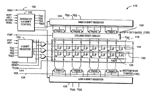
An integrated circuit active matrix display die 116 is shown schematically in
FIG. 2. The integrated circuit display die I 16 has been diced from a single
wafer 114
along with a selected number of replicated circuits. incorporated into the
integrated
circuit display die 116 are a display matrix circuit 1 I8, a vertical shift
register 120, a
horizontal shift control I22, a pair of horizontal shift registers 124 and
126, and a
plurality of transmission gates 128 and 130.
A video signal high line i32 and a video signal low line I34 carry analog
video signals from a digital to analog amplifier to the; transmission gates
128 and 130
located above and below the display matrix circuit 1:18. In a preferred
embodiment,
the transmission gates above the display matrix circuit are p-channel
transmission
gates 128 and are-connected to the video high (VIDHf) line 134. The
transmission
gates 130, which are located below the display matri;~c circuit 118 in a
preferred
embodiment are n-channel transmission gates 130 and are connected to the video
low
(VIDL) line 134.
The transmission gates 128 and 130 are controlled by the horizontal shift
registers 124 and 126. The p-channel transmission gate 128 is controlled by
the high
horizontal shift register 124 and the n-channel transmussion gate 130 by the
low
horizontal shift register 126, as in the embodiment shown in FIG. 2. The
horizontal
shift registers 124 and 126 are controlled. by the horizontal shift control
I22. The
horizontal shift registers 124 and 126 select the column to which that bit or
segment
of the video signal is sent as further explained below.
CA 02354018 2001-06-06
- WO 00/36583 _ 13 _ PCT/US99/29b73
The display matrix circuit 1 I 8 has a plurality of pixel elements 138. For
example, in a QVGA display there would be 76,80t> (320 x 240) active pixel
elements. There may be additional pixel elements which would not be considered
active, as explained below. Each pixel element 138 has a transistor 140 and a
pixel
S electrode 142. The pixel electrode 142 works in conjunction with a
counterelectrode
144 and an interposed layer of liquid crystal 146, as best seen in FIG. 9, to
form a
pixel capacitor 148 for creating an image.
In addition to selecting the column which receives the signal by use of the
horizontal shift registers 124 and 126 as described above, the row needs to be
I O selected. The vertical shift register 120 selects the now. The row line 1
SO from the
vertical shift register 120 is connected to the gate of each of the
transistors 140 to
turns on the pixels of the row. With the pixels turned on for one row, and a
column
1 S2 selected by one of the horizontal shift registers lL 24 and 126, a single
pixel is
selected and the video signal drives the liquid crystal or allows the liquid
crystal of
I S the pixel element to relax.
The microdisplay 1 I O has the image scanned in row by row in a progressive
fashion. In a preferred embodiment of the QVGA, tile image is scanned or the
pixel
electrode voltage is set pixel element by pixel element. Two pixel elements
can be
set at one time, with an odd or even receiving a VIDIH signal I32 using high
20 horizontal shift register 124 and the other row (i.e. the even or odd)
receiving a ViDL
signal 134 using low horizontal shift register 126, as explained below with
respect to
FIG. I 1. It is recognized that other configurations such as shown in FIG. 10,
can be
used where the display is broken into segments and acre supplied
simultaneously. It
is also recognized that multiple pixel electrodes can be scanned in the same
clock
2S cycle, if the display uses multiple VIDH and VIDL inputs.
The display matrix circuit 118 has a column reset circuit 154. The column
reset circuit 1 S4 is used for both power down reset, as explained below with
respect
to the FIGS. 24 and 2S and initialization as explained below with respect to
FIGS.
23A and 23B. In initialization, the column reset circuit 1 S4 sets the voltage
to each
30 pixel electrode 142 to the voltage which results in the; liquid crystal
relaxing to the
CA 02354018 2001-06-06
WO 00136583 - 14 - PCT/US99I296'73
clear state. The column reset circuit 154 is used before each subframe or
frame as
explained below.
FIG. 3 illustrates a timing diagram for a mi.crodisplay using column
inversion. The video signal is sent to the IC displaEy die 116 both as actual
video and
inverted video. The p-channel transmission gates 128, as seen in FIG. 2,
receive
actual video and the pixels supplied by these gates are driven between the
common
voltage (Voo~, the voltage applied to the countere:lectrode, and the supply
voltage
source (VDD). The n-channel transmission gates 130 receive the inverted video
and
the pixels supplied by these gates are driven between VCOM and the supply
voltage
i 0 sink (VEE). In one subframe, one column receives video and the adjacent
columns
receive inverted video. In the next subframe, the columns receiving the video
and
inverted video are switched. After the entire frame is scanned into the
display and
there is a delay to allow the liquid crystal to twist, the backlight is
flashed to present
the image. The delay to allow the liquid crystal to ttwist is further
explained below.
1 S In a preferred embodiment, VDD is approximately 11 volts, VEE is
approximately 2
volts and VCOM is approximately 7.0 volts. There is a slight voltage
difference
between the voltage signal center voltaged (VVC) and VcoM to accommodate an
offset voltage in the liquid crystal. The technique of alternating the video
on each
column is called column inversion and helps prevent a DC voltage from building
up
20 on the liquid crystal material and additionally prevents cross talk. In
addition to
column inversion, other similar inversion techniques are row inversion, frame
inversion and pixel inversion.
Other timing diagrams are discussed below which feed the video and flash
the backlight in a different manner to present the image.
25 The flat panel display, also referred to as a rr~icrodisplay 110, is
assembled in
several major assemblies wherein in each assembly may have several steps.
Referring to FIG. 4, the wafer 1 I4 is a SOI (Silicon on Insulator) wafer on
which the
integrated circuit display die I 16 is laid. The display circuit 116
transferred to a
glass sheet 158 and is lifted off the wafer 114. The backside of the display
circuit
30 1 I6 is processed. In addition to the display circuit I 16, an ITO (Indium
Tin Oxide)
wafer 160, as seen in FIG. 6, having the counterelectrode 144 is manufactured.
The
CA 02354018 2001-06-06
WO 00/36583 - 15 - PCT/US99129673
display circuit 116, the ITO wafer 160 and the liquid crystal 146 are
assembled in a
display assembly 162. The display assembly 162 is. assembled into a module
assembly I64.
The forming of the IC display die 1 I6 is illustrated in FIGS. 5A-5D. One of
the transistors 140 of the display matrix circuit 118 is shown being formed
with a
thin film single crystal silicon layer i72 over an inso~zlating substrate 174
as seen in
FIG. 5A. The silicon layer 172 over the insulating soubstrate 174 can be
formed by
recrystallization of the silicon layer or by using a bonded wafer process in
which a
first silicon wafer is bonded to a second silicon wafer with an insulating
oxide layer.
The second wafer is thinned to form a silicon-on-insulator structure suitable
for
display circuit fabrication and transfer to an optically transparent
substrate.
Additional details on fabrication of the display is described in U.S. Patent
Application No. 08/215,555 filed March 21, 1994 arid titled "Methods of
Fabricating
Active Matrix Pixel Electrodes" which issued as U.S. Patent No. 5,705,424 on
January 6, 1998, and U.S. Patent Application No. 08/966,985 filed November 10;
1998 and titled " Color Sequential Reflective Micro<iisplay," the contents of
which
are incorporated herein in their entirety by reference.. A thermal oxide 176
also
overlies a portion of the single crystal silicon layer 172. The insulating
substrate 174
is carried by a Silicon (Si) wafer 178.
A layer of Si3N4 180 is formed as an anti-reflection layer over the insulating
substrate 174 and the thermal oxide 176 as illustrated in FIG. 5B. The pixel
electrode I42, a poly-silicon electrode, is formed over the Si3N4 layer 180
and is in
contact with the thin film single crystal silicon layer 172.
Referring to FIG. SC, a Boron Phosphorus Silica Glass (BPSG) layer 184 is
formed over the circuit. A portion is etched away and an aluminum terminal 186
is
added. Referring to FIG. SD, a layer of Phosphorus Silica Glass (PSG) 188 of
Si02
is formed over the BPSG 134 and the aluminum ternunal 186. A titanium (Ti)
black
matrix 190 is located over the transistor as a Iight shield. A silica
passivation 192 is
formed over the entire wafer. The wafer is ready for the next assembly
process.
CA 02354018 2001-06-06
WO OOl3b5$3 - I 6 - PCTlUS99I296~3
In a separate process, the ITO wafer I60 having a counterelectrode i44 is
formed. FIG. 6 illustrates the ITO wafer having a layer of glass I98, and the
counterelectrode 144 (an ITO layer).
With the circuitry formed and the ITO wafer I60 formed, the two are ready to
be joined together. The circuitry device 116 is then transferred to an
optically
transparent substrate 204 as shown in FIG. 7A. A transparent adhesive 206 as
described in greater detail in U.S. Patent No. 5,256,,562, the contents of
which are
incorporated herein by reference, is used to secure the circuit to the
substrate 204.
The layer, Si Wafer 178, seen in FIGS. SA-SD, to vvhich the insulating
substrate 174
I O was initially attached, is removed.
The insulating substrate 174, also referred to as a buried oxide layer, is
etched
in the location over the pixel arrays I42 as illustrated in FIG. 7A. The
buried oxide
layer not located over the pixel arrays is Left, thereizi creating a series of
pools 208.
In a preferred embodiment, the buried oxide layer is O.SUm and thinned by
0.21tm to
0.31Zm in the pool areas over the pixel arrays. By only thinning the pixel
arrays, the
applied voltage to the liquid crystal is increased without compromising the
back-gate
effect to the transistors (TFTs).
An alternative integrated circuit display die 116 is shown in FIGS. 7B and 7C.
Referring to FIG. 7B, the insulating substrate 174 is~ etched, a layer of
Si3N4 180 is
formed over the insulating substrate 174 and the thermal oxide 176. The pixel
electrode 142, a poly-silicon electrode, is formed over the Si3N4 layer and is
in
contact with the thin film single crystal silicon layer 172. The rest of the
wafer is
formed in the method described above.
After, the circuitry device 116 is transferred to an optically transparent
substrate 204 as seen in FIG. 7C. The insulating substrate 174, also referred
to as a
buried oxide layer, is etched. The buried oxide is thinned until the Si3N4
layer 180,
as seen in FIG. 7B, is reached. The Si3N4 layer 180 is removed by wet etch
phosphoric acid process. The pixel electrode i42 is in contact with the liquid
crystal
146.
It is recognized that the insulating substrate L 74 can be etched in the
location
where the pixel electrodes 142 are to be located to the silicon wafer i78. The
Si3Na
CA 02354018 2001-06-06
WO 00/36583 - 17 - PCTIUS99/29673
layer is located on the silicon wager 178. The buried oxide does not need to
be
thinned after the circuit device 1 I6 is transferred to the optically
transparent substrate
204. The Si3N4 layer 180 is removed as described above.
It is also recognized that the series of pools; 208, such as shown in FIG 7A,
can be thinned to the Si3N4 layer 180. The Si3N4 layer 180 with a wet etch
phosphoric acid process.
An alignment layer 210 of SiOx is deposited on the buried oxide and the
counterelectrode illustrated in FIGS. 6 and 7A. Th.e alignment layers 210
align the
liquid crystal as described below.
A frame adhesive 2I2 is placed around each display area as illustrated in FIG.
8. in addition, a silver paste is located in one spot sin each display, so
that the
counter electrode is connected to the circuit when joined. A fill hole is left
for filling
the liquid crystal, as described below. The frame a,3hesive has a plurality of
spacer
balls. The spacer balls are 3-4 ltrn in diameter. The TFT glass and the
counterelectrode glass are pressed together. The spacer balls ensure that the
layers
are spaced 1.8pm apart when the bonding pressure its asserted. There are no
spacers
in the active matrix area. The combined wafers are then cured. While in a
preferred
embodiment spacer balls are used, it is recognized a. spacerless display can
also be
made using other spacer technology such as posts.
After curing, the two sheets of glass, the TF'.C glass 204 and the
counterelectrode glass 198, are scribed and broken. The two glass layers are
scribed
and broken on two opposite ends and staggered such that the TFT glass 204
appears
shifted to the right relative to the counterelectrode glass 198 in FIG. 9.
The individual displays are placed in a holding tray and dipped into liquid
crystal to fill the space between the buried layer and the counterelectrode.
The liquid
crystal 146 is located between the alignment layers 2;10. The fill hole is
then filled.
That is the final step of the display assembly.
The module assembly consists of attaching a flex cable 214, a pair of
polarizers 216 and mounting them into a module 218.. Referring to FIG. 9, a
sectional view of a display I 10 is shown. For clarity, the elements of the
display are
not shown to scale, only one pixel element is shown and certain elements have
not
CA 02354018 2001-06-06
WO 00!365$3 = 18 - PCTIUS99/29673
been shown. The display i 10 has an active matrix portion 220 including the
pixel
element 138 spaced from the counterelectrode 144 'by the interposed liquid
crystal
material layer 146. Each pixel element 138 has a transistor 140 and a pixel
electrode
142. The active matrix portion 220 can have aluminum light shields 224 to
protect
the transistor (TFT) 140 if the active matrix is used for projection requiring
high
luminance light. The counterelectrode 144 is connected to the rest of the
circuit by
solder bumps 226. The matrix 220 is bounded by a pair of glass substrates 198
and
204. An additional pair of glass plates 228 are located outboard of the active
matrix
portion 220. The glass plates 228 are spaced from the polarizer 216. The space
defines an insulation layer 230. The module 2I 8 of the display 110 is a two-
piece
case which contains the active matrix portion 220, tlhe glass plates 228 and
the
polarizers 216. A room temperature vulcanization (RTV) rubber 232 helps
maintain
the elements in the proper position in the case.
Each of the glass substrates 198 and 204 has one of the polarizers 2I6 on the
side opposite the layer of liquid crystal 146.
In order to get the liquid crystal to respond more quickly, the distance
between the counterelectrode and the oxide layer is 2.0 lzm at the pools 208.
The
narrow distance between the two elements results in less liquid crystal that
has to
twist to allow light to pass. However, the narrowing; of the distance results
in
additional problems including the viscosity of some liquid crystals making it
difficult
to fill the display. Therefore, the selection of the proper liquid crystal
requires an
evaluation of the liquid crystal properties.
There are many characteristics that must be taken into account in selecting
the
desirable liquid crystal. Some characteristics include; the operational
temperature
range, the birefringence (delta n = n~-no), the operational voltage, viscosity
and
resistivity of the liquid crystal. With respect to viscosity, flow viscosity
and
rotational viscosity are two areas that are examined. The preferred ranges are
a flow
viscosity of less than 40 centipoises (cp) and a rotational viscosity less
than 200cp in
the temperature range of 0° C to 70°C.
Another characteristic that is examined in selE;eting a liquid crystal is
delta n.
The value of delta n depends on the cell gap and the liquid crystal pretilt
angle at the
CA 02354018 2001-06-06
WO 00/36583 _ 19 _ PCT/US99/29673
two surfaces. The pretilt angle at the two surfaces is influenced by the
alignment
layer of SiOX deposited on the buried oxide and the counterelectrode. For a
2pm gap
a delta n of greater than 0.18 is preferred and a delta n of 0.285 is desired.
For a
large gap a different delta n is required. For a gap <>f5pm a delta n in the
range of
0.08 to 0.14 is desired.
in addition to viscosity and delta n (fin), the; liquid crystal's threshold
voltage
and the voltage holding rate are criteria to be examined when selecting a
liquid
crystal. In a preferred embodiment, the threshold voltage is less than 1.8
volts, and
preferably approximately 1.2 volts. The voltage hooding ratio is preferably
greater
than 99%.
Other characteristics that are desired are easy alignment and stability to UV
and high optical intensity. If required, the delta n cm be compromised in
order to
achieve a lower viscosity and lower operation valtal;e.
In a preferred embodiment, the liquid crystal. chosen was a SFM
(superfluoriated material). In preferred embodiments, the liquid crystal
selected was
one of TL203 and MLC-9100-000 marketed by Merck.
Liquid crystal is formed of a chemical chain which extends from the two
surfaces. The alignment layers 210 of SiOx as seen in FiG. 7A, are deposited
on the
buried oxide 174 and the counterelectrode 144, or the pixel electrode 142 and
the
counter electrode 144 in FIG. 7C1 are oriented in a preferred embodiment at
90° to
each other. The alignment layers 210 give the liquid. crystal 146 a pre-
alignment.
The alignment layers 210 have thickness of approxinnately 500 Angstrom.
The chain of liquid crystal twists and untwists depending on the voltage to
the associated pixel electrode. This twisting in relation to the polarization
plates
results in the liquid crystal going between a white or clear state and a dark
state.
While depending on the relation of the liquid crystal and the polarization
plates, the liquid crystal can either look clear or dark in the relaxed
position and
conversely dark or clear in the driven state. In a preferred embodiment, the
liquid
crystal looks clear in the relaxed position and dark in the driven state.
As indicated above, the microdisplay 110 can have an active matrix array of
different numbers of pixels. FIG. 10 shows schematically an alternative
circuit
CA 02354018 2001-06-06
WO 00/36583 _ 20 _ PCTIUS99I29673
active matrix display die 240 for (640 x 480) pixel display. In contrast to
the
embodiment shown in FIG. 2, the display is split into quadrants which feed
simultaneously and independently. The integrated circuit display die 240 has a
display matrix circuit 242, a pair of vertical shift registers 244, a
horizontal shift
S control 246, a quadruplet of horizontal shift registers 248, and a plurality
of
transmission gates 250.
The analog video signals from a digital to a':ialog amplifier are carried on a
quadruplet of video signal lines 2S2 to the transmission gates 2S0 located
above and
below the display matrix circuit 224. The integrated circuit display die 240
has a
column reset circuit ZS4, similar to the column reset circuit I S4 discussed
above.
The display matrix circuit 242 has elements similar to those discussed above
with
respect to FIG. 2 and shown in more detail in FIG. 20A.
It is recognized that in both smaller and larger arrays, such as 480 x 320 and
1280 x 1024, it may be desirable to split the display in sectors and drive
individual
1S sectors independently. Another description of a display with a multiple
channel
driver is described in U.S. Patent Application Serial; No. 08/942,272 filed on
September 30, 1997 and titled "Color Display System for a Camera," the entire
contents being incorporated herein by reference.
FIG. 11 shows an integrated circuit display die 2S8 for a microdisplay for low
voltage video in which video is fed to the even columns of the display from
one side,
above in FIG. I 1, and the video for the odd columns is fed from the other
side.
Incorporated into the integrated circuit display die 258 are a display matrix
circuit
260, a vertical shift register 120, a horizontal shift control 122, a pair of
horizontal
shift register 124 and 126, and a plurality of transmission gates 262. The
2S transmission gates 262 may be implemented with a complimentary pair of N-
channel
1020 and P-channel I022 transistors.
A pair of video signal lines 264 carries analog video signals from a pair of
digital to analog amplifiers 356, as discussed in furt3her detail with respect
to FIG.
39B, to the transmission gates 262. The transmission gates 262 are controlled
by the
horizontal shift registers 124 and I26. The horizontal shift registers 124 and
I26 are
controlled by the horizontal shift control 122. The horizontal shift registers
select the
CA 02354018 2001-06-06
WO 00/36583 - 2i - PCT/lJS99/29673
two columns to which that bits or segment of the video signal are sent by the
inputted
video signal. In contrast to the integrated circuit display dies shown in FIG.
2 and
10, the two pixels, one in an even column and one in an odd column, are
written
simultaneously .
The display matrix circuit 260 has a plurality of pixel elements I28 similar
to
the previous embodiments. Each pixel element 138 has the transistor 140 and
the
pixel electrode 142. The pixel electrode 142 works in conjunction with the
counterelectrode 144 and the interposed layer of liquid crystal 146, as best
seen in
FIG. 20A, to form the pixel capacitor 148 for creating an image.
I0 In addition to selecting the column which receives the signal by use of the
horizontal shift register 124, the row needs to be selected. The vertical
shift register
120 selects the row. The row line 150 from the vertical shift register i 20 is
connected to the gate of each of the transistors 140 to turn on the pixels of
the row.
With the pixels turned on for one row, and two columns 152 selected, each by a
respective horizontal shift register 124 or 126, the tv~ro pixels are selected
and the
video signal drives the liquid crystal or allows the liquid crystal of the
pixel element
to relax.
In contrast to the integrated circuit display die 116 of FIG. 2; while there
still
two horizontal shift registers and two video signal lines, each video signal
line
receives both a video signal and an inverted video si~~al. The signal is
switched
each frame or subframe and is referred to as frame inversion. In addition, the
voltage
to the counterelectrode {Vco~ is switched every frame or subframe as explained
below. The integrated circuit display die also has a column reset circuit 154.
In low
voltage video (LW), which will be described in greater detail below, the
voltage of
the counterelectrode is switched and initialization occurs at the beginning of
the
subframe. While the integrated circuit display die 258 which writes to two
pixels at
the same time is discussed with LW, neither requires the other.
The image on the microdisplay 110 is viewed in a preferred embodiment by
shining a light through the liquid crystal I46 or backlighting the liquid
crystal 146.
FIGS. 12A, 12B, and 12C show a backlight system 266.
CA 02354018 2001-06-06
WO 00/36583 - 22 ~ PCT/US99/296'73
An exploded view of a preferred embodiment of the backlight system 266
relative to the display 110 is shown in FIG. 12A. A plurality of LEDs 270
backlight
are mounted on circuit board 268. Preferably, three LEDs are used to provide
three
colors. The circuit board 268 with the LEDs 270 is held by a backlight housing
278.
Between the backlight housing 278 and the display 110, a brightness
enhancement
film 280, such as the "BEF" film available from 3hZ Corporation can optionally
be
used along with a diffuser 282. As seen in FIGS. 1:2B and 12C, the circuit
board 268
mounted on a first side of housing 278 and the bacl~;light active area is
defined by the
diffuser 282 on a second side of the housing 274.
The microdisplay 100 and the backlight sysi:em 266 are coupled with a lens
system 284. FIG. 13A is a perspective view of the ;~ssernbled display module
286.
The exploded view of FIG. 13B shows the elements. of the system 286 in detail.
The
backlight reflector is positioned in backlight housing 278 which can be
adhered
directly onto the display 110 with an epoxy adhesive or with a plurality of
clips 288.
The display is held by a display holder 290 which c:~n also serve to define
the visual
border for the active area of the display as seen by the user thrnugh a
transparent
window 292. The transparent window 292 which is generally considered part of
the
lens system 284, is carried by an optics holder 294. The optics holder 294 in
addition retains a color correction element 296, and a lens 298. An optional
second
lens may be located in the optics holder 294.
The optics holder 294 is slideably located in a housing element 300. A pin
302 carried by the optics holder 294 couples the holder 294 to a ring 304,
such that
rotation of the ring 304 translates the optics holder 2'94 along an optical
axis 306. A
holding panel 308, which retains the ring 304 to the housing element 300 also
secures the display holder 290, which is referred to as a module 218 in FIG:
9. The
assembled display module 286 as illustrated in FIGS. 13A and 13B has a volume
of
less than i5cm3.
The assembled display module 286 fits snugly within an external housing
such as a viewfinder housing 862, such as that shown in FIG. 43, or within the
other
device housings as described herein, such as in FIG. ~41. These small high
resolution
CA 02354018 2001-06-06
WO 00/36583 _ 23 _ PCTlUS99/29673
displays require magnification such that when held in a user's hand within the
range
of 0.5 inches to 10 inches of the user's eye, a clear image is provided.
Referring to FIG. 14A, the lens 298 for magnifying the image of the
microdisplay I 10 and carried in the optics holder 2!~4 ofFIGS. 13A and 13B is
shown. For a QVGA {Quarter VGA 320 x240) display with a 0.24 inches diagonal
microdisplay, in a preferred embodiment the lens 298 has an outer diameter 312
of
about 30.4mm and a thickness 314 at the optical axiis 206 of about 8mm. The
lens
298 has an inner surface 316 that receives light from the display and has a
curved
diameter of about 21.6 mm, and viewing surface 31.8 has a diameter 320 of
about
22.4. A peripheral edge 322 of the lens 298 is used to hold the lens 298 in
the optics
holder 294 and has a thickness 324 of about 2 mm and a radius 328 of about 4
mm.
While in a preferred embodiment, the lens 298 is made of acrylic, it is
recognized
that the lens 298 could be made of polymer material or glass. This particular
example of such a lens has a 16 degree field of view and an ERD (eye relief
distance)
of 54mm.
FIG. 14B is a cross sectional view of an alternative assembled display module
286 with lens 298. The lens 298, along with the transparent window 292 and the
color correction element 296, not shown in FIG. l4Et, is retained by the
optics holder
294.
The backlight housing 278 has three LEDs 2'70. The rnicrodisplay 1 i 0 is
within the module 218 interposed between the holding element 300 and the
backlight
housing 278.
Another preferred embodiment of a 1.25 inch. diameter lens system 330 with
a larger field of view is illustrated in FIG. 14C. Three lens elements 332,
334 and
336 enlarge the image on the display 110.
The color correction element 296 can be a transparent molded plastic
kinoform having a contoured surface with circular steps that introduce phase
corrections into the incident light. The conf guration of a preferred
embodiment 296
in which the single lens 298 is positioned adjacent the kinoform, color
correction
element, 296 for a QVGA display 110 is illustrated irE FiG. 15 with dimensions
in
millimeters. The kinoform 296 can be made of an acrylic material molded to
form a
CA 02354018 2001-06-06
WO OOI36583 _ 24 _ PCT/US99/29673
concave surface 296a facing the lens. The surface 296a can have an anti-
reflective
coating thereon to increase the transmission: The concave surface is divided
into a
number of zones of different radii and width. Each zone is separated by a step
in the
surface. The QVGA display preferably has between 150 and 300 zones whereas a
640 x 480 display has between 500 and 1000 zones.
Other preferred embodiments of optical systems for color displays are
described in application U.S. Serial No. 08/565,OSE~ filed on November 30,
1995, the
entire contents of which is incorporated herein by reference. Additional
details on
optical systems for color displays are described in LJ.S. Serial No.
08/966,985 filed
on November 10, 1997 of Jacobsen et al. and titled "REFLECTIVE
MICRODISPLAY FOR PORTABLE COMMUNICATION SYSTEM", the contents
of which is incorporated herein in its entirety by reference.
In producing the image both the twisting and untwisting of the pixel segments
of liquid crystal, as described in more detail below and the LEDs 270 of the
backlight system 266 needed to be controlled the Ll?Ds 270 are flashed to
produce
the image as explained below. In addition, to the fl:~shing, it may be
desirable to
vary the intensity.
When LEDs 270 are produced, the intensity for a given current will vary from
LED to LED or lot to lot. In attempting to balance the colors of the three
LEDs, red,
blue and green, one technique is to connect a poten~~orneter to each LED and
adjust
to get the proper balance of color temperature.
FIG. 16A is a cross sectional view of a backlight system 340 with a detector
342. The backlight system 340 has a backlight housing 278 to which a circuit
board
344 and the diffuser 282 are attached. A plurality ofLEDs 270 are attached to
the
circuit board 344. The detector 342 is Located on the; opposite side of the
circuit
board 344. An aperture or glass rod 346 allows light to pass through the
circuit board
344 from the LEDs 270 to the detector 342. In a preferred embodiment, the
detector
342 is made from silicon. It is recognized that other visible light sensors
like photo
resistive material can be used.
FIG. 16B is a schematic of a circuit 348 that controls the current to the LEDs
270. The circuit 348 has a display logic circuit 350, which controls the LEDs
270
CA 02354018 2001-06-06
WO 00/365$3 - 25 - PCT/US99/29673
through a multiplexes 352 which selects the LED 2.70. In a preferred
embodiment,
the multiplexes 352 is part of the display logic circuit. The multiplexes 352
is
controlled by the display Iagic circuit 350. The display logic circuit 350 is
further
discussed below with respect to the microdisplay I I0.
In addition to being connected to the multiplexes 352/LED 270, the display
logic circuit 350 is connected to a memory 354. In a preferred embodiment, the
memory is a 24 bit memory which holds predetermined values of intensity levels
for
the red, green and blue LEDs 270. A digital-to-analog converter 356 receives
the
digital value from the memory 354 and produces an analog signal representing
the
I0 intensity level.
The brightness control 362 may be used to adjust the analog signal from the
converter 356. In a preferred embodiment, the brightness control 362 may be a
potentiometer at the output of the converter 356. In an alternative
embodiment, the
brightness control may be connected to the full-scale control of the converter
356.
I S A feedback control circuit 358 compares the signal from the detector 342
to
the analog intensity signal from the converter 356 or brightness control 362,
and
produces an output signal far the LED current drive circuit 360. The feedback
control circuit 358 adjusts its output signal so that tine LED intensity
measured by the
detector 342 matches the intensity value set by the converter 356 and
brightness
20 control 362. In a preferred embodiment, the LED cuGrrent drive circuit 360
uses a
transistor 366 and resistor 368.
While in most environments it is desired to have the display as bright as
possible, especially in bright sunlight, there are certain situations where it
is desirous
to Iower the intensity of the display such that the person using the display
preserves
25 their night vision, such as an aircraft or a ship at night.
The backlight in the display transitions from .a normal mode to a night or low
light ambient mode. In a normal mode, the LED(s) for normal light are used,
such as
a single amber, green, or white LEDs for a monochrome display and red, blue,
and
green LEDs for a color sequential display.
30 For daylight operation, the "day" LED(s) would be on to provide the display
to be readable in ambient sunlight. If the ambient Iight Ieve1 decreases, the
LED(s)' .
CA 02354018 2001-06-06
W0 00/365$3 - 26 - PCTNS99l29673
intensity could be decreased to provide an image r~rith brightness comfortable
to
view. At some point with lower light ambient, a call for a decrease in the LED
intensity would result in the turning off of the "day" LED and the turning on
of the
"night" LED; further reductions in display brightnc;ss would result in
decrease of the
"night" LED intensity until arriving to some minimum or at some point the LED
is
fumed off. Referring to FIG. 16B, an ambient light sensor 369 connects to the
brightness control 362 to vary the intensity of the L,EDs 270. The ambient
Iight
sensor 369 also connects to the display Iogic circuii: 350 such that the Iogic
circuit
350 can switch to single color "night" LED.
Increasing the display brightness would be the reverse of this, consisting of
first increasing the "night" LED brightness until some crossover point where
the
"night" LED was turned off and the "day" LED fumed on. Further increasing of
the
display brightness would only increase the "day" LED brightness.
Dependent on the environment in which the microdisplay is located, the
"night" LED is either a red LED or a blue green LE:D. While red is typically
considered better for maintaining a person's night vision, the red light is
more
detectable using night detection gear.
It is recognized that the night illumination sa~urce can be chosen either from
a
class of sources that do not emit infrared and near infrared frequencies, or a
filter that
removes infrared and near infrared frequencies can be interposed between the
night
Iight source and the remaining structure.
While the intensity, style or color of a Iight source may be dependent on the
ambient Iight, the level of ambient Iight does not gerAerally effect the color
sequential
process described below. The circuitry for backlight was discussed above.
Circuitry
for controlling the microdisplay 110 is described below.
The configuration of the display for a monochrome or a color sequential
display is generally the same with the same pixel pitch or size. This is in
contrast to
other types of color displays where there is an individual pixel for each of
red, green
and blue. The distinction in the display is the Iight source not the
microdisplay 110.
In a monochrome display a single light source is required, wherein in a color
sequential display there are three distinct light sources (e.g., red, green
and blue). In
CA 02354018 2001-06-06
WO 00/36583 _ 27 - PCT/US99/29673
that there are three distinct colors, each color must flash in order to
produce most
images, in contrast to one flash for monochrome. Ii; is recognized that for
monochrome, it may be desirable to leave the LED on or to pulse the light
emitting
diode (LED) as described below.
In sequential color displays, the display panel is triple scanned, once for
each
primary color. For example, to produce color frames at 20 Hz; the active
matrix
must be driven at a frequency of 60 Hz. However, in order to reduce flicker it
is
desirable to drive the active matrix to have a frame rate of 60 frames per
second,
since at over 60 Hz, visible flicker is reduced. In a color display a
preferred frame
rate is a minimum 60 frames per second which results in 180 sub-frames per
second,
in that each frame has a red, a blue and a green sub-frame. In contrast for
the
monochrome display where there is only a frame not three subframes, the frame
rate
can be higher and in a preferred embodiment the Prune rate is 72 frames per
second.
It is thus recognized that while a display for a color sequential display is
substantially
similar to one for a monochrome display, the sub-frame rate needs to be
substantially
faster to achieve the desired results in color sequential.
Referring back to FIGS. 2 and 3, the image its scanned into the active matrix
display 110 by the vertical shift register 120 selecting the first row, by the
row going
low, and the horizontal shift register 124 or 126 selecting column by column
until the
entire row has been written to.
In a column inversion mode, which is the preferred mode for the integrated
circuit display die 116 shown in FIG. 2, the video for each pixel element 138
is
alternated from video entering throughout the p-channel transmission gates 128
from
the video signal high line 132 and inverted video entering through the n-
channel
transmission gate 130 from the video signal low line; 134. The switching back
and
forth from video to inverted video in each column prevents DC voltage buildup
on
the buried oxide 174 and the liquid crystal 146.
When the f rst row is done, the vertical shift register 120 selects the second
row. This continues until the last row is selected. The horizontal shift
register 124
or I26 selects column by column until the Last column in the last row has been
written to. There is therefore a set time delay between when the first pixel
(i.e., the
CA 02354018 2001-06-06
WO 00/36583 _ 2g _ PCT/US99129673
first row, first column) and when the last pixel (i.e., the last row, last
column) has
been written. in a preferred embodiment, the delay from writing the first
pixel to the
last pixel is approximately 3 milliseconds.
As indicated above in describing the assemlbly of microdisplay 110, the liquid
crystal does not respond instantaneously to the change of voltage. The delay
for the
liquid crystal to respond is illustrated in FIG. 17. The state of the liquid
crystal 146
is dependent on the voltage of the pixel electrode 142, commonly referred to
as Vp;xel
370, and the voltage of counterelectrode 144, commonly referred to as V~oM
372.
With Vp;xe, 370 initially equal to V~oM 372, in framf; 378 as seen in FIG. 17,
there is
no voltage drop across the iiqnid crystal and the liquid crystal 146, as seen
through
the polarizers, is clear, as illustrated in transparence; graph. When Vp;X~,
370 goes to a
voltage, +V or -V, 374 there is a voltage drop or difference across the liquid
crystal;
the liquid crystal is driven black as seen in frames 3~80.
The change is not instantaneous since it takes the liquid crystal a set time
to
rotate. This time is a function of several factors including the type of
liquid crystal
and the temperature. The voltage is shown alternating since the voltage is
inverted
on the pixels to prevent a DC charge building on the liquid crystal.
If after reaching the steady state black, Vp;Xer is set to VcoM, the liquid
crystal
returns to the clear state. Like the translation from t;lear to black, the
change is not
instantaneous. The change of state from black to clear takes longer than when
the
liquid crystal is being driven to black as seen in frarnes 382. FIG. I7 shows
it takes
over 2 %Z times as long to go from black to clear as it takes to go from clear
to black.
In a preferred embodiment using the preferred liquid crystal at room
temperature; the
time to drive from white to black is approximately 4~ milliseconds and the
time for
the liquid crystal to return to white is approximately 10 milliseconds.
As indicated above, in order for the color display to reduce flicker, there
needs to be 180 subframes per second or less than 6 milliseconds per subframe.
Therefore at 180 subframes per second, the liquid crystal cannot go from black
to
clear in a subfiame.
An example where a red image or pixel is desired is shown in FIG. 18A. The
upper graph shows the voltage of the pixel electrode 142, Vp;xel 370. The
voltage
CA 02354018 2001-06-06
WO 00/36583 - 29 - PCT/US99/29673
Vp~Xe, 370 is set to a voltage to relax the liquid crystal to clear or drive
the liquid
crystal to black. It is desired that the liquid crystal is clear when the red
LED flash
and black or opaque when the green or blue LED flLashes. Therefore, to obtain
the
red pixel, the voltage of pixel electrode 142, Vp;xei =s 70 is set to VCoM for
the
subframe 384 which is associated with the red flash of light and another
voltage for
the subframes 386 which are associated with the green and the blue flashes.
With the
microdisplay 110 having 180 subfi-ames per secondl, the eye blends red flash
with the
dark opaque periods therein producing a red pixel.
If the liquid crystal starts as clear in the first: subframe 384a, it is
capable of
being driven black in the next subframe 386a, the subframe associated with the
green
flash. The display circuit continues to drive the liquid crystal black for the
next
subframe 386b associated with the blue flash. When the display circuit for
that pixel
sets the voltage for that pixel electrode 142, Vp;~e~ 3'70 to VCOM, the liquid
crystal is
allowed to relax. However, the liquid crystal 146, ~~s represented in the
illustration,
does not get to a clear state by the time the subframe 384b is done. In the
illustration
shown in FIG. 18A, the liquid crystal only gets to about fifty percent (50%)
clear. in
the next subframe 386c, the green subframe, the liquid crystal 146 is driven
black
again. Therefore, the liquid crystal for this red pixel never gets to its
completely
clear state before the flash. A maximum brightness or conixast is never
achieved.
With a color sequential display, even when t:he display is of a static image,
the display is dynamic since the display is sequencing through the red image,
the
green image, and the blue image.
Referring back to FIG. 3, if the liquid crystal had a fast enough response to
twist or untwist or if the subframe was a longer timE; period, even the last
pixel 388
written to, as represented by the end of the write bo:K, would be settled in
the final
position before the flashing of the LED. However, the liquid crystal does not
respond quickly enough to allow settling at the framie or subframe speeds
required to
prevent flicker as illustrated in FIG. 18A. In that the pixels are written to
sequentially, the first pixel 390 is written to (i.e., driven to twist or
allowed to relax)
a set time before the last pixel 388. In a preferred embodiment, the time
between
writing to the first pixel 390 and the last pixel 388 is approximately 3
milliseconds.
CA 02354018 2001-06-06
WO 00/3b583 _ 30 _ PCT/tlS99I29673
Therefore, the liquid crystal 146 associated. with the last pixel 388 and the
liquid crystal 146 associated with the first pixel 388 do not have the same
amount of
time to respond prior to the flashing of the backlight.
With the twist of the liquid crystal different at the two pixels, there is a
different amount of light passing through the liquid crystal and therefore the
contrast,
the luminance, the color blend can vary from one corner to another of the
display.
For example, if a display had an intermediate color such as yellow at the
first pixel
and the last pixel, the color would not be identical.
An example of producing a yellow pixel which is created by allowing the red
flash and the green flash to be seen and not the blue flash is shown in FIG.
18B. The
FIG. 18B illustrates that the video signal sets the voltage for each pixel
electrode
142, V~;xe, 370, to VcoM for the red subframes and fi7r the green subframes,
and to
another voltage for the blue subframes. Therefore 'the video for the pixel is
set to
drive the pixel black for the blue subframe and allow it to relax for the red
and the
green subframes, as represented by the square wavc;. In the first subframe
392a in
FIG. 18B, the blue subframe, the liquid crystal for iboth the first pixel 390
and the
last pixel 388 are shown at a steady state black. Th.e first pixel 390
receives its signal
at the beginning of the red subframe 394a and the liiquid crystal begins to
relax. The
last pixel 388 receives its signal at some time later, 3 milliseconds in a
preferred
embodiment, and the liquid crystal begins to relax at that time. The liquid
crystal
146 related to the first pixel 390 and the last pixel 388 are at different
points in the
transition to clear when the red LED flashes, therein producing different
levels of
red. In the embodiment shown in FIG. 18B, the ne:!ct color to flash is green
and
therefore the pixel electrodes 142 associated with first and last pixels 390
and 388 do
not change voltage in the transition to the subframe 396x. Therefore the
liquid
crystal associated with both the first and the last pixel 390 continues to
transition to
clear. When the LED for green flashes, the liquid crystal for the two pixels
390 and
388 are in different points of transition to clear, therefore there is a
different level of
green. In addition, because the green flash occurred after the red flash and
the liquid
crystal had more time to transition, the amount of green that is visible is
greater than
the amount of red, therein resulting in a greenish yellow.
CA 02354018 2001-06-06
- WO OOI36583 _ 31 _ PCT/US99/29673
Still referring to FIG. 18B, the next subframc~ is the blue subframe 392b. The
pixels 390 and 388 are driven black. The first pixel 390 once again receives
its
signal near the beginning of the subframe and in that in a preferred
embodiment it
takes 3 milliseconds for the liquid crystal to turn black, the liquid crystal
146 is black
before the flash of the blue LED. The last pixel 388 receives its signal near
the end
of the subframe and is still transitioning to black when the blue LED flashes.
Therefore, the last pixel 388 in this subframe 392b has some blue in its
yellow.
In the next frame, the next red subframe 394b, the liquid crystal 146 is
relaxing, therein turning to clear. The last pixel had been previously driven
black,
therefore as it transitions to clear, the last pixel will once again lag
behind the first
pixel.
FIG. 19A illustrates a display control circuit 400 for practicing the LW
method. The digital control circuit 400 takes an image from a source and
displays
the image on the microdisplay 110. The digital control circuit 400 has a
processor
402 which receives image data at an input 404. The processor 402 sends display
data
to a memory 406 and/or a flash memory 408 via a timing control circuit 410.
The
image data can be in a variety of forms including serial or parallel digital
data, analog
RGB data, composite data, or s-video. The processor 402 is conf gored for the
type
of image data received, as is well known in the art. l:n the preferred
embodiment
shown in FIG. 19A, the signal is digital or is converted to digital before
entering the
timing control circuit 410.
The timing control circuit 410 receives clock and digital control signals from
the processor 402. The timing control circuit 410 controls both the
mierodisplay 110
and the backlight system 266. The timing control cv~cuit 410 transmits control
signals to the backlight 266 along a plurality of lines 411. The control
signals from
the timing control circuit 410 control the flashing of the LEDs 270 in
relation to the
image on the microdisplay 110. The tirriing, the duration and intensity of the
flash of
LEDs 270 is controlled.
The image data travels from the timing control circuit 410 to the microdisplay
110 through a digital-to-analog converter 412. The analog image data/signal is
sent
along two paths. One of the paths has the signal pass through an inverter 412.
The
CA 02354018 2001-06-06
WO 00136583 _ 32 _ PCT/US99/29673
analog video signal and the inverted analog video signal are alternatively fed
to the
microdisplay 10, with a switch 416 alternating the input on each subframe. In
addition, the common voltage (Vco",~ which enters the display 110 and applied
to
the counterelectrode I44 is alternated between the two values by a switch 418.
The
switches 416 and 418 for alternating the video and t:he VcoM to the display
are
controlled by a frame control line 420 from the timing control circuit 410.
The timing control circuit 410 transmits control signals, such as vertical
start
pulse; vertical clock, horizontal start pulse, and horizontal clock, to the
display 110
along lines 422 and 424. Lines 428 direct ready, reset, write enable, output
enable,
color enable, address and data signals to memory 4C>6/408 to control delivery
of
image frames to the display 110.
Referring to FIG. 19B in conjunction with FIG.19A, the voltage of the
counterelectrode 144, the common voltage (Vco,,,~ alternates between two
voltages.
The video signal is alternating between actual video signal and inverted. In
contrast
to the column inversion in the previous embodiment; where the video signal is
inverted in every column, in LW the video signal is inverted only every frame.
In a preferred embodiment, V~oM alternates t~etween a video high voltage
(V~ of 6 volts and a video low voltage (V~) of l .:i volts. Therefore, V~oM
alternates between a high voltage V~, referred to as VcoM HIGH and a low
voltage
V"I", referred to as VCOM Low. The video signal voltage fluctuates between
V"I, and
V~. Both the supply voltage source (VDD) and the supply voltage sink (VEE) are
off set from V"a and V',,., by 1.5 volts, ie. VDD is 7.:5 volts and VEE is 0
volts.
These offset or headroom increase pixel transistor conduction in the on state
and
decrease pixel transistor leakage in the off state.
With V~oM high as in frame 432a, the actual video signal is scanned.or
written 434 into the matrix circuit/microdisplay 110. After a rest time or
delay 436
to allow for the liquid crystal 146 to twist towards the desired position, a
flash period
438 occurs where the LED backlight 266 flashes to present the images.
Prior to the next frame, subframe 2, 432b, V~oM goes low. With V~oM
switching to the low voltage, the image that has just 'been scanned is erased
because
CA 02354018 2001-06-06
WO 00/36583 - 33 - PCT/US99I29673
the voltage across the pixel changed. However, since the flash period 438
ended and
the LED backlights 270 are not on, the loss of the innage is not seen.
With V~o;,s low in frame 432b, the inverted video signal is scanned or written
434 into the matrix circuitlmicrodisplay 110. Simil~~rly after the rest time
436, a
flash period 438 occurs to present a refreshed or nevv image.
Prior to the next frame 432c, V~oM goes high. With V~oM switched to the
high voltage, Voo~ high, the image that was scannecl in is erased. The actual
video
signal is written 434 into the microdisplay 110 with V~oM high. A delay occurs
and
the flash of the LED.
A. schematic of pixel element 138 is shown in FIG. 20A. The pixel element
138 has the transistor (TFT) 140 through which the video is fed. The
transistor
(TFT) 140 is controlled by a signal from the vertical shift register 120.
There is a storage capacitor 442 which holds the charge and in a preferred
embodiment connects to another row line 150, the previous row line (N-1). In
addition, the liquid crystal 146 in proximity to the pixel electrode 142 acts
as a
capacitor 444 and a resistor 446. The buried oxide 174 interposed between the
pixel
electrode 142 and the liquid crystal 146 acts as a second capacitor 446. The
counterelectrode 144 which has the common voltage; VCOM switches back and
forth as
described above.
If the display is a color display, the LEDs 270 of the backlight 266
sequentially flash the distinct colors. In addition, three screen scans, one
for each
color LED 270, comprise a frame and the V~oM alternates each screen, sub
frame.
The delay time before beginning the flash an<i the flash time are shown as
identical in FIG. 19B. However, both the delay time (the delay for response
time of
the liquid crystal) and the flash time can depend on tlhe specif c color to be
flashed.
The delay time depends on when the liquid crystal associated with the last
pixel to be
written has sufficient time to twist to allow that speciific color to be seen.
The
duration of the flash, or the point that the flash must'be terminated, depends
on when
the liquid crystal associated with the first pixel to be written of the next
frame has
twisted sufficiently that Light from the backlight is visible to the viewer.
CA 02354018 2001-06-06
WO 00/36583 - 34 - PCT/US99/29673
The timing control circuit 4 i 0, as seen in FIfG. I 9A, can vary the flash
duration and the delay or response time depending on the color that is to be
flashed.
In addition, the current to the backlights 266 can be; varied to adjust the
intensity of
the color. If desired, a color control line 520 can be added to the timing
control
circuit 410 to allow the user to vary the color.
In a preferred embodiment, V~,~ fluctuates every 5-6 milliseconds. It takes
approximately 3 milliseconds to write/scan the image. The LED flashes for a
time
period of about 0.5 milliseconds. There is a waiting; period between writing
to the
last pixel and the flash of about 1.5 milliseconds, such as represented in
FIG. 19B. It
IO is recognized that it may be desirable to vary the delay time before
flashing the LED
or vary the length of the LED flash depending on the color LED to be flashed.
Less time is needed to write with a smaller storage capacitor and therefore a
smaller pixel TFT can be used. If the liquid crystal has a fast enough
response, the
storage capacitor can be eliminated and the capacitance of the liquid crystal
becomes
the storage capacitor. in addition, with no storage capacitor a larger
aperture is
possible. With a larger aperture and increased aperture ratio, the image will
be
brighter for the same cycling of the backlight or the total power used can be
reduced
with the same image brightness.
Referring to FIG. 20B, a portion of the display control circuit of FIG. 19A
with an enlarged schematic of one pixel 138 is shown. The pixel 138 is charged
by
the horizontal shift register 124 selecting the column 152 by turning a
transmission
gate 262 and the vertical shift register 170 selecting a row 150. The video is
written
to the pixel and the liquid crystal begins to twist and become optically
transmissive.
After the entire display has been written and there h~~s been a delay before
the LED
flashes, the Vco~ , i.e., the voltage to the counterelectrode 144, is switched
from high
to low or vice versa by the frame control line 420. t~,t the same time, the
video signal
is switched from actual video to inverted video or vice versa, so that the
video will be
switched for the next frame.
The liquid crystal can be twisted to become either optically transmissive or
optically opaque. The orientation of the polarizers ajFfect whether the liquid
crystal is
driven to white, transmissive, or to dark, opaque.
CA 02354018 2001-06-06
WO OOJ36583 - 35 - PCT/US99129673
Referring to FIG. 21, the top graph 452 illustrates the switching of the
voltage to the counterelectrode 144, V~oM every subframe. The voltage switches
between 6 and i.5 volts in a preferred embodiment. The resetting of the V~oM
changes the reference voltage for the pixel 138.
The second line 454 illustrates the video signal that switches between a video
and an inverted video signal. The video signal varies from a voltage
representing
clear to a voltage representing black. When VcoM is at the low voltage, 1.5
volts in a
preferred embodiment, the voltage for clear would equal V~oM, 1.5 volts and
the
voltage for black in a preferred embodiment is 6 volts. This second line
represents
I O the video signal for black which is offset voltage of 4.5 volts from the
voltage of
'VcoM~
The middle two lines 456 and 458 of FIG. 21 illustrate the voltage offset on a
particular pixel element. The upper of the two lines 456 illustrates a pixel
written to
black and the lower line 458 illustrates the same pixel written to clear.
15 Referring the third line 456, the pixels start as clear, ie. the voltage
offset
between the pixel electrode and the counterelectrode is zero. When the proper
column and row is selected for the pixel, the pixel el~trode voltage is set at
4.5 volts
offset from the Voorl, ie. 1.5 volts wherein VcoM is 6 volts in a preferred
embodiment. The liquid crystal begins to be driven t:o the dark position. At a
set
20 period of time afterwards, the pixel has been written and the LED is
flashed. When
the VcoM is switched from 6 volts to 1.5 volts, as indiicated in the first
line 452, the
offset of this pixel electrode goes from 4.5 to zero thE;rein resulting in the
liquid
crystal relaxing back towards the clear direction. When the video signal is
again
written to the pixel to drive it black, the video signal is offset once again
by 4.5 volts
25 but in this case it is a video signal of 6 volts. The flash of LED occurs a
set time
period afterwards. When V~oM once again is flipped from I.5 to 6 volts, the
offset
returns to zero between the pixel electrode and the counterelectrode and the
liquid
crystal begins to relax back towards clear. This pattern continues to repeat.
With respect to the fourth line 458 in FIG. 21, which illustrates the pixel
30 written to clear, the pixel starts as black with the offset voltage between
the V~oM
and video being 4.5. When the pixel electrode is written to clear, the offset
voltage
CA 02354018 2001-06-06
WO 00/36583 _ 36 _ PCTIUS99129673
between the V~oM and the pixel electrode becomes zero and the liquid crystal
begins
to rotate towards a clear position. At a set period afterwards, the LED
flashes. When
the voltage of the counterelectrode is switched fronn 6 volts to 1.5 volts the
offset
between the pixel electrode and the counterelectrocle goes from zero to 4.5
volts and
S the liquid crystal begins to be driven black. When the pixel electrode is
next written,
the voltage to the pixel electrode is set to 1.5 volts which is equivalent to
the
counterelectrode voltage and an offset voltage of zero therein the liquid
crystal
begins to relax back to a clear state. The LED is fleshed a set time
afterwards. When
the voltage of the counterelectrode is next switched. from 1.5 volt to 6
volts, the
offset of the voltage between the pixel electrode and the counterelectrode
becomes
4.5 volts again and the liquid crystal associated witlh this pixel electrode
is driven
towards black. When the video signal for this pixel. electrode is written to
white the
voltage is set to 6 volts and the voltage offset between the pixel electrode:
and the
counterelectrode is zero volts and the liquid crystal begins to relax back to
the clear
position. This pattern continues to repeat.
The fifth line 460 in FIG. 21 represents a video signal for the pixel. For
simplicity and clarity, the video signal is shown constant for the entire
frame even
though the video signal only at the time period associated with that pixel is
relevant.
The first subfrarne 464x, the video signal is to drive the liquid crystal
black therein
the voltage of the signal is 4.5 offset from VcoM or 1..5 volts. In the next
subframe
464b, the signal to be written is for clear therein the voltage is set to the
voltage; of
VcoM the voltage remains at 1.5 volts since the voltage V~oM is once again 1.5
in that
VcoM h~ switched to 1.5 volts. The third subframe 464c the video is once again
set
for clear, however, in that VcoM has switched from 1..5 volts to 6 volts, the
video
signal likewise is flipped or inverted from 1.5 to 6 volts so that the offset
is
maintained at zero. In the fourth subframe 464d shown, the video signal is
written
such that the pixel will turn back to black therein the; video needs to be
offset by 4.5
volts in a preferred embodiment from that of VcoM and VooM in this subframe is
1.5
volts and the video is set to 6 volts.
The sixth and bottom line: 462 shows the video of the pixel using the video
from the above line 460 written at the proper location indicated by the dashed
CA 02354018 2001-06-06
WO 00/36583 _ 37 _ PCT/US99129673
vertical fines 472. The video pixel is initially offset from that of the
counterelectrode
by zero volts until the pixel electrode is written to black therein putting an
offset of
4.5 volts. The liquid crystal associated with the pixel I38 is driven, twisted
to black.
The flash is indicated by the dashed vertical line 474 however, in that the
pixel
electrode has been driven so that the liquid crystal has rotated to black
therein the
red flash is not seen. Upon the counterelectrode switching from 6 volts to 1.5
volts,
the pixel begins to relax to clear since the voltage offset between the
counterelectrode and Vpixel is zero. Upon the pixel electrode being written,
it is
written to clear however, the voltage has akeady had a zero offset so there is
no
I O change. When the flash occurs for subframe 464b in that the liquid crystal
has
rotated to a clear position, the green flash is seen at tile pixel.
Upon the counterelectrode switching to 6 volits from 1.5 volts at the
beginning of subframe 464c, the offset between the voltage of the pixel
electrode and
the counterelectrode is 4.5 volts therein the liquid crystal begins to be
driven to the
1 S black state. When the pixel electrode is written to clc;ar (white) the
voltage of the
pixel electrode is set to 6 volts wherein the offset from the voltage and the
counterlectrode is zero and the liquid crystal begins t~o relax back to clear.
When the
flash occurs the liquid crystal has been moving towards the clear state and
the blue
LED light is seen.
20 Upon the counterelectrode being switched from 6 volts back to i.5 volts at
the start of the next subframe 466a, the offset between the counterelectrode
and the
pixel electrode is 4.5 volts and the liquid crystal begins to be driven black.
When the
pixel electrode is written to again, to the black state, the voltage of the
pixel electrode
does not change therein when the flash occurs the liquid crystal blocks the
light and
25 the red LED is not seen therein the green and blue lights are seen to give
a cyan
color.
FIG. 22 illustrates the creation of a yellow pixel for the first pixel and the
last
pixel, similar to what is shown in FIG. 18B, with the voltage of the
counterelectrode
144 V~oM switching after each subframe. While generally referring to a frame
as a
30 red, green and blue subframe, the first color flash and order is merely a
preference.
The video for the pixel is set to drive the pixel black i:or the blue subframe
468b and
CA 02354018 2001-06-06
WO O~136583 - 3$ - PCTlUS99129673
allow it to relax for the red 468r and the green subfi°ames, as
represented by the
square wave. In the first subframe in FiG. 22, the ~nlue subframe 468b, the
Liquid
crystal for both the first pixel and the last pixel are shown at a steady
state black.
The first pixel 390 receives its signal at the beginning of the red subframe
and the
liquid crystal begins to relax. The last pixel 384 receives its signal at some
time
later, 3 milliseconds in a preferred embodiment, and the liquid crystal begins
to relax
at that time. The liquid crystal related to the first pixel and the last pixel
are at
different points in the transition to clear when the re;d LED flashes, therein
producing
different levels of red as in FIG. 18B. However, in contrast to the previous
embodiment, the switching of the voltage to the cou~nterelectrode resets the
clear
pixels to black. This is represented by the downward slope between the red
subframe
468r and the green subframe 4688.
The next color to flash is green. The first pixel receives its signal at the
beginning of the green subfi~ame 468g and the liquid crystal begins to relax.
The last
I S pixel receives its signal at some time later, 3 milliseconds in a
preferred embodiment,
and the liquid crystal begins to relax at that time. V~~hen the LED for green
flashes,
the liquid crystal for the two pixels are in different points of transition to
clear,
therefore there is a different level of green. However, in contrast to the
previous
embodiment, the liquid crystal does not have more tame to transition prior to
the
flash of the green LED compared to the red LED, since the voltage to the
counterelectrode is switched every frame. The color is thus more uniform in
that
both the first pixel and the last pixel have the same ratio of red to green.
Still refernng to FIG. 22, the next subframe :is the blue subfi~ame 468b. The
pixels are driven black by the switching of the voltage to the
counterelectrode VcoM,
as represented by the slope between the green subfr~un~ 468g and the blue
subframe
468b. In contrast to the previous embodiment, both the first pixel 390 and the
Last
pixel 388 are driven black at the same time by the switching of the voltage to
the
counterelectrode. When the individual pixel is written to, the pixel is
written to
black so there is no change. The last pixel 388 is therefore not still
transitioning
when the blue LED is flashed. With the switching o~f the voltage to the
CA 02354018 2001-06-06
WO 00/36583 _ 39 _ PCTNS99/29673
counterelectrode VooM, while there are still variations of luminosity from the
top to
the bottom, there is now uniform color.
In an alternative embodiment, the storage capacitor 422 for each pixel
element 138 is connected to the black matrix 190 instead of the previous row
line
150 for anew LVV display. With the storage capacitor 422 connected to the
black
matrix 190, the microdisplay 110 can progress from the top to the bottom or
from the
bottom to the top. In that the video data is stored digitally, the video can
be scanned
alternatively from the top to the bottom and then scanned from the bottom to
the top
to average out the time between writing and the flashing for the total image.
To achieve good color purity, the liquid cry;ctal must complete its transition
to
the proper state prior to or during a settling phase 4'76, which is
illustrated in FIG.
23A. Otherwise, the liquid crystal state is effected by the position, state,
of liquid
crystal in the previous subfrarne (e.g, the green flash will depend on its
state during
the red field). This "color shift" effect appears at the bottom of the display
first,
IS since those pixels are the last to be updated during tlhe Write phase 472.
As indicated above, LW (low voltage video) is a combination of the
switching of the voltage of the counterlectrode 144 ;end the initialization.
Initialization is discussed below.
Initialization occurs prior to the writing of the image to the display. An
initialization phase (Init) 478 is shown in FIG. 23A just before the write
phase 472.
The initialization phase 478 takes advantage of the fact that the black-to-
white and
white-to-black liquid crystal transition times are different in the preferred
embodiment. In a preferred embodiment in which the black-to-white transition
is
slower, all pixels are initialized to the white state at the beginning of the
field by
setting the voltage to the pixels Vp~L to the same voltage as the
counterelectrode,
VcoM, as referred to as initialization, after flashing the backlight.
In one preferred embodiment, the odd rows axe first set to VcoM with the even
rows subsequently set to VcoM. With the pixel electrodes set to VcoM, the
liquid
crystal begins to relax to the clear state, if the liquid crystal associated
with the pixel
is in some other state. This gives those pixels which will be written to clear
(white)
pixel a head start, so that the Settle phase 476 need b~e only as long as the
faster clear
CA 02354018 2001-06-06
WO 00/36583 _ 40 _ PCT/US99I29673
(white)-to-black transition. (It is recognized that the optimal initialization
state will
depend on such particulars as liquid crystal chemishy, alignment, and cell
assembly,
and that initialization to black, clear, or intermediate; gray levels might be
preferred
for a given display).
Once the voltage to the pixel electrodes Vp~~L has been reset to VooM in the
initialization phase 478, the writing phase 472 begins and the first pixel
receives its
signal and begins to transition. Each pixel receives iits signal until the
last pixel
receives its signal. The liquid crystal associated witlh each pixel is
relaxing, rotating
to the clear state, until that specific pixel receives the signal. The first
pixels will
have the majority of the writing period to get to their desired position and
the
initializing of the pixel to VCOM will have minimal ei:fect. However, the
pixels which
receive their signal last will be clear or near clear prior to receiving their
signal. As
indicated above it takes less time to drive black than relax white (clear).
Therefore,
with the end pixels being clear, the response time is quicker driving to black
than if
the pixels were black and needed to relax to clear.
The drive electronics quickly update all pixels in the array. First, the data
scanners drive all column lines to the appropriate initialization voltage. An
initialization switch 482 is associated with each column. FIG. 23B shows
switches
implemented with p-channel MOS transistors; it is recognized that n-channel
transistors, complementary MOS pairs, or other configurations could be used.
Second, the select scanners 484 select multiple rows simultaneously as
described in
relation to the power down reset circuitry. The control logic is modified to
support
the initialization operation. In power down reset the columns are all set to
VDpin .
contrast to the initial voltage as in the initialization phase 478.
A preferred method according to the invention which we refer to as low
voltage video (LW) improves the image by overcoming several of the image
quality
problems discussed above. An integrated circuit display die 258 for a LW
display
is shown in FIG. 11.
It is recognized that the switching of the voltage to the counterelectrode
V~oM
or initializing can be done individually or in combination. However, in LW
(low
voltage video) both the switching of the voltage to the counterelectrode and
the
CA 02354018 2001-06-06
WO 00/36583 _ 41 _ PCTIUS99/29673
initializing are done. The combination allows for lower voltages and takes
advantage
of the fact that the response time driving white to black is quicker than the
response
time driving black to white.
FIG. 23C illustrates a LVV microdisplay with both the switching of the
voltage to the counterelectrode and the initializing of the pixels to clear.
In contrast
to FIG. 21 and similarl to FIG. 22, a first and last pixel are discussed. The
top two
graphs 462 and 454 are similar to the top two graphs of FIG. 21.
The top graph 452 illustrates the switching of the voltage to the
counterelectrode 144, VcoM every subframe. The voltage switches between 6 and
1.S
volts in a preferred embodiment. The second Line 4454 illustrates the video
signal
which switches between a video and an inverted vi<ieo signal. The video signal
varies from a voltage representing clear to a voltagE; representing black.
This second
line 454 represents the video signal for black, whic3h is an offset in voltage
of 4.5
volts from the voltage of VcoM.
The third Line 460 of FIG. 23C, similar to th.e fifth line in FIG. 21,
represents
a video signal for the pixels. For simplicity and clarity, the video signal is
shown
constant for the entire frame even though only at the time period associated
with the
pixels is relevant.
In addition, while the video signal is shown at either totally black or
totally
clear, it is recognized that the video signal can be at a level in between.
For example,
if the voltage of the video signal is 4 volts using the preferred embodiment
voltages,
the video is some gradient between clear and black, resulting in a gradient or
grey
scale.
In the first subframe 486r of the third line 4Ei0, the video signal is at a
level to
drive the liquid crystal black therein the voltage of the signal is 4.5 volts
offset from
VcoM or 1.5 volts. In the next subframe 486g, the signal to be written is for
clear,
therein the voltage is set to the voltage of VcoM; the voltage is once again
l.Svolts in
that VcoM has switched to l.5volts. The third subframe 486b, the video is once
again
set for clear, however, in that VcoM has switched from 1.5 volts to 6 volts,
the video
signal likewise is flipped or inverted from 1.5 to 6 volts so that the offset
is
maintained at zero. In the fourth subframe 488r shown, the video signal is
written
CA 02354018 2001-06-06
WO OOI36583 _ 42 . PCTJUS99/296~3
such that the pixel will tum back to black therein th.e video needs to be
offset by 4.5
volts in a preferred embodiment from that of VCOM; VcoM in this subframe is
1.5 volts
and the video is set to 6 volts.
The fourth line 490 and the fifth line 492 show the video of the pixel using
the video from the third line 460 written to the pixel at the respective time.
The
fourth line 490 illustrates the writing to the first pixel 390 that is written
to in the
microdisplay I 10. The fifth line 492 illustrates the writing to the last
pixel 388 that
is written to in the microdisplay 110.
Both pixels are written to black, therein putting an offset of 4.5 volts. The
pixel TL 388 is written at a set time after T,. In a preferred embodiment, the
delay
between the writing to the first pixel 390 and to the last pixel 388 is 4.2
milliseconds,
during which all the interposed pixels are written.
The sixth line 494 and the seventh line 496 illustrate the position of the
liquid
crystal associated with the first pixel element (T,) 490 and last pixel
element (TL)
492 respectively. The flash is indicated by the dash line. However, in that
the pixel
electrode has been driven so that the liquid crystal has rotated to black as
seen in the
sixth and seventh lines 494 and 496, the red flash is not seen.
Referring to the fourth and fifth lines 490 and 492, upon the counterelectrode
switching from 6 volts to 1.5 volts entering subframe 4868, the voltage offset
between the counterelectrode and Vpixel is zem andl the liquid crystal begins
to relax
to clear, as seen in the sixth and the seventh lines 494 and 496.
In that the switching of the voltage to the coimterelectrode sets the pixel
electrodes to a voltage representing clear, the initialization does change the
pixel
electrode or the transitioning of the liquid crystal. I:~pon the pixel
electrode being
written, it is written to clear however similar to the effect of the
initialization, since
the voltage has already had a zero offset, there is no change. When the flash
474
occurs, in that the liquid crystal has rotated to a clea~~ position as
illustrated in lines
six and seven 494 and 496, the green flash is seen at the pixels.
In the next subframe 486b, upon the countere;Iectrode switching to 6 volts
from 1.5 volts as illustrated in the first line 452 of F1:G. 23C, the offset
between the
voltage of the pixel electrode and the counterelectrode is 4.5 volts therein
the liquid
CA 02354018 2001-06-06
WO 00136583 _ 43 _ PCT/US99/29673
crystal begins to be driven to the black state as illustrated in the downward
line in
both the fourth line 490 and the fifth line 492. The liquid crystal begins to
rotate
towards black as seen in lines 494 and 496. However, shortly after the
switching of
the voltage to the counterelectrode all the pixels are initialized to the
clear
position/voltage as illustrated by the upward line in both the fourth line and
fiffih Line.
The liquid crystal beings to relax to clear state as illustrated in the sixth
line and the
seventh line 494 and 496. The initializing occurs less than 100 microseconds
after
the switching the valtage counterelectrode in a prefi~rred embodiment.
Upon the two pixel electrodes being written., the pixels are written to clear;
however, in that the voltage is already a zero offset, there is no change to
the voltage
to the pixel electrode. The liquid crystal continues to relax to the clear
position as
illustrated in the sixth line 494 for pixel T, or remains in the proper
position as when
the last pixel 388 would be written as illustrated in the fifth line 492 and
the seventh
line 494. When the flash occurs, the liquid crystal for both pixel T, and T~,,
as
illustrated by the sixth line 494 and the seventh line 496 of FIG. 23C, have
settled in
the clear state and the light of the blue LED light is seen.
In the next subframe 488r, upon the counterc~lectrode being switched from 6
volts back to 1.5 volts, the offset between the counterelectrode and the pixel
electrode is 4.5 volts as illustrated by the downward line in the fourth line
490 and
20 the fifth line 492 and the liquid crystal begins to be .driven towards the
black state as
illustrated by the downward sloping line in the sixth. and seventh lines 494
and 496.
However, shortly after switching the voltage to the counterelectrodes, all the
pixels are initialized to the clear position/voltage as illustrated by the
downward line
in both the fourth Line and the fifth line 490 and 492. The liquid crystal
begins to
relax to the clear state as illustrated in the sixth line and the seventh line
49'4 and 496.
The liquid crystal of the first pixel T, does not get back to the completely
clear position prior to the pixel being written 498 as seen in the sixth line
494 of FIG.
23C. The writing to the pixel, T, sets the pixel electrode to a 4.5 volt
offset over the
counterelectrode voltage of 1.5 volts as seen in the fourth line and the first
line
respectively. The setting of the pixel electrode to a voltage representing
black results
in the liquid crystal being rotated to black.
CA 02354018 2001-06-06
WO 00/36583 ,~ ~ _ PCTNS991Z9673
The liquid crystal of the last pixel TL returns to the completely clear
position
prior to the pixel being written 500 as illustrated in the seventh line 496.
The writing
to the pixel TL in subframe 488r, as illustrated in th<~ fifth line 492 to
black, results in
the liquid crystal being rotated to black. In that the liquid crystal can be
driven
S quickly to black in contrast to relaxing to clear, the liquid crystal
associated with the
last pixel 288, pixel TL along with first pixel 290 T,, is in proper position
prior to the
flash of the red LED. However, in that the liquid crystal has rotated to
black, the red
flash is not seen.
The process is continued. In contrast to the previous embodiment, in that
each pixel electrode has been set to an offset of zero which results in the
liquid
crystal rotating towards clear, the liquid crystal is either clear or moving
towards
clear when the image is written to the pixel. In that the liquid crystal can
be driven
from clear to black in the setting time between the v~rriting of the last
pixel TL and the
flash, the liquid crystal is either at or in close proximity the desired state
when the
flash occurs. This results in the color being more uriifanm and the contrast
and
brightness improved over the previous embodiments.
In LW, the switching of the voltage to the counterelectrode allows for a
reduced voltage range. The initialization allows the liquid crystal associated
with
each pixel to relax, rotate to the clear state, until that; pixel receives the
signal. The
first pixels will have the majority of the writing period to get to their
desired position
and the initializing of the pixel to VcoM will have minimum affect. However,
the
pixels which receive their signal last will be clear or nearly clear prior to
receiving
their signal. As indicated above, it takes less time to drive black than relax
clear
(white) in the embodiment discussed. Therefore, with the end pixels being
clear, the
response time is quicker driving to black than if the 3pixels were black and
relaxing to
clear. (It is recognized that the optimal initialization. state will depend on
such
particulars as liquid crystal chemistry, alignment, and cell assembly, and
that
initialization to black, white, or gray levels might be preferred for a given
display).
In a preferred embodiment, the writing of each subframe takes 4.2
milliseconds. The settle, flash; LW of switching the voltage to the
counterelectrode
and initialization combines for 1.3 milliseconds. The settle time in a
preferred
CA 02354018 2001-06-06
- w0 00/36583 - 45 - PCT/US99129673
embodiment is approximately 1.0 milliseconds before the beginning of the
flash.
While the flash can extend into the beginning of the writing of the next
subframe, in
that LW affects the pixel by beginning to turn the liquid crystal, the end of
the flash
may need to be based on the beginning of LW. However, the use of LW results in
a shorter settling time requirement.
In another embodiment associated with the die of FIG. 11, the writing of each
subframe takes 1.64 milliseconds. The settle, flash, LVV of switching the
voltage to
the counterelectrode and initialization combines for 3.92 milliseconds. The
settle
time ina preferred embodiment is approximately 3.12 milliseconds before the
beginning of the flash.
Referring to FIG. 24, in normal operation the; voltage of the pixel is
fluctuating. The voltage at the point (V,~, as seen in FIG. 20A, between the
buried
oxide and the liquid crystal generally follows the pixel voltage, but is lower
because
of the drop across the buried oxide and drops because of the resistance of the
liquid
crystal (RL~). When powering off, VDn drops to zero. The pixel voltage (VP~ is
unable to discharge through the p-channel pixel TFT and drops. VA which is
coupled
to VPs drops likewise. If a sufficient time transpires, VA will return to zero
due to
the Roc.
However, if the power is funned back on to th.e display prior to the natural
discharge time, a portion of the image may be seen fir several seconds. VPs
goes
positive when the power comes on and since VA is coupled it goes positive
above and
creates a black image. VA returns to normal in several minutes due to RL~. The
reason the image may be retained even with switching the voltage to the
counterelectrode and the initialization relates to the uiherent capacitance of
the
buried oxide. The buried oxide does not have an associated inherent resistance
and
the voltage shift by pixel causes a DC build-up. This DC build-up will
eventually
decrease due to R~,c.
A display circuit is illustrated in FIG. 25. In this embodiment, a digital
circuit 506 is used to control color sequential display operation. The
processor 402
receives serial digital image data at 404 and sends di::play data to memory
406 via
the timing control circuit 410. The timing control circuit 410 receives clock
and
CA 02354018 2001-06-06
w0 OOI36583 _ 46 _ PCTIUS99I29673
digital control signals from the processor 402 and b~ansmits control signals
to the
backlight 266 and display 110 along lines 411 and 422, respectively. Lines 428
direct ready, reset, write enable, output enable, color enable, address and
data signals
to memory to control delivery of image frames to the display 110.
S An analog comparator 508 samples the voltage of the main power in real
time. When the voltage drops below the level to nun the circuit plus some
margin
which is set by a reference 510, a reset signal {PDR*) is asserted low. On
receipt of
the PDR* signal the display circuitry will place VDT, on all the column tines,
see FIG.
2, and activate all the row lines. The normal timing; continues for two or
more
cycles, therein sequentially activating all the even and odd rows. This clocks
the VDn
signal on the column lines into every pixel.
Refernng back to FIG. 20A, VpD will also charge the pixel storage capacitor
442. As indicated above, in a preferred embodiment, the storage capacitor 442
is
connected to the previous row Iine 150. By activating all the even row Iines,
(i.e.,
driving them low) and not the odd row lines (i.e., maintaining high), the
storage
capacitors 442 on the even rows will be discharged to 0 volts. (VpD is high
logic
level). On the next cycle the odd rows storage capacitors will be discharged.
Because the storage capacitor is several times larger than the pixel
capacitor, the
voltage on the storage capacitor will then discharge the pixel capacitor to 0
volts. At
this point the display can be de-energized without any residual charge left on
either
the storage or pixel capacitor.
FIG. 26 illustrates a timing diagram. The system power is turned off at time
T1 and is shown as a classical discharge as the logic continues to run powered
by the
bypass capacitors. The comparator senses the threshold voltage level and
asserts the
PDR* low, at time T2. The additional row enable signals are then asserted and
completed at time T3. No additional Iogic or signals are required after T3 and
the
power is allowed to randomly discharge. The power. down reset works with the
modes discussed above including column inversion .and the switching of the
voltage
to the counterelectrode VcoM.
CA 02354018 2001-06-06
WO 00136583 - 47 - PCT/US99129673
As indicated above, the temperature of the display and in particular the
temperature of the liquid crystal effects the response and the characteristics
of the
display.
Referring back to FIG. 19A, the display circuit has an additional line, a
temperature sensor line 512, which runs from the display 110 to the timing
control
circuit 410. The active matrix comprises a pluralit~i of pixels arranged in
columns
and rows. Heat is preferably absorbed substantially uniformly throughout the
liquid
crystal material. However, there may be local temperature variations due to
the
nature of the image being displayed as well as display and heater geometry and
environmental conditions. Temperature sensors can be distributed throughout
the
active matrix region including around the perimeter' of the active matrix
including the
corners and also disposed near the center of the active matrix. The use of a
temperature sensor is described in U.S. Patent Application Serial No.
08/364,070
filed December 27, 1994 and is incorporated herein by reference. A temperature
sensor 514 is illustrated in the corner of the display in FIG. 27A. As
indicated above,
temperature sensors can be distributed throughout the active matrix region.
The characteristics of the liquid crystal material are effected by the
temperature of the liquid crystal. One such example; is the twist time of
twisted-
nematic liquid crystal material, which is shorter when the liquid crystal
material is
warm. By knowing the temperature of the liquid crystal, the timing contrnl
circuit
410 can set the duration and timing of the flash of tine backlight 260,
therein
achieving the desired brightness and minimizing power consumption.
Referring back to FIG. 20B, during normal operations, the vertical shift
register 120 has only one row on, so that as the horizontal shift register 124
moves
from column to column only one pixel is affected. After the last pixel on a
row is
addressed, the vertical shift register 120 switches thE; active row. The
display 110
can be placed in a heat mode where each row 1 SO is turned on and has a
voltage drop
across the row to create heat. In the embodiment shown in FIG. 20B, an end 516
of
each row line is connected to Vpp and the end near the shift register is
driven low
thereby creating a voltage differential across each line. Heat is generated at
a rate
P=VZ/R, where R is the resistance of the parallel combination of row Lines and
V the
CA 02354018 2001-06-06
WO 00/36583 - 4g _ PCTIUS99129673
voltage differential across the row lines. In normal operation, only the
selected line
which contains pixels to be driven low generates he;~.t, not the entire
display.
Referring back to FIG. 19B, with the common voltage (VCOM) high, the actual
video signal is scanned into the matrix circuit. After a delay to allow for
the liquid
crystal to twist into position, the LED backlight 266 is flashed to present
the image.
Prior to the next screen or subframe, a heat cycle 51$ occurs where all the
row lines
are driven such that there is a voltage differential across the row. The
heating can
occur while V~flM and the video are being alternated and inverted,
respectively, by
the frame control line 420, as seen in FIG. 19A. FICi. 19B shows a heating
cycle S18
after each subframe, but the number and time period. of heat cycles can depend
on the
temperature of the liquid crystal as determined by the temperature sensor 514.
In
cold environments, the digital circuit can have a waxen-up cycle where the
heater is
turned on prior to the first painting of the screen.
Refernng to FIG. 27A, a schematic of the di,>play 110 and the digital to
analog converter 412 are shown. The display has a horizontal shift register
124, a
vertical shift register 120, and switches 262 similar to what is illustrated
in FIG. 20B.
In addition, and in contrast to FIG. 208, FIG. 27A illustrates a heating gate
522.
Referring to FIG. 27B, for pixels which have. p- channel TFTs, the heating
gate 522 has a series of n-channel TFTs. Typically when writing to the display
only
the row being written to is on (V=0). When not writing to the display, all the
rows
are VDD. When the n-channel TFTs turned on; by applying VpD to a row line 150
results in current flowing from the inverter associated with the vertical
shift register
I70 through the row to the n~hannel TFT and heat is dissipated along the
entire
row. The source is connected to VSS, which is zero. :It is also recognized
that the
display 110 can have several extra rows outside the typical array to assist in
uniform
heating.
Likewise for pixels which have n-channel TF'Ts, refernng to FIG. 27C the
heating gate 522 has a series of p-channel TFTs. Typically when writing to the
display only the row being written to is on (V=VDD). When not writing to the
display, all the rows are approximately zero (0) volts.. When the p-channel
TFTs are
CA 02354018 2001-06-06
WO 00/36583 - 49 - PCTIUS99I29673
turned on by setting the gate to zero (0), there is a voltage drop across the
row of
VDD~
It is recognized that LW (low voltage video) including the switching of the
voltage to the counterelectrode VcoM and the heating; of the display discussed
above
can be used independently. Heating can be incorporated into the embodiments
described with respect to FIG. 2. While an internal heater is preferred, it is
recognized that a separate heater can be used with tree temperature sensor.
In the embodiments shown in FIGS. 27B and 27C, a DC voltage drop ~V
develops across the display as current flows through. the row lines 150 to
create the
heat. Depending on the length and frequency of the heating cycles, a DC field
can be
created that affects the performance of the Liquid Crystal. An alternative
embodiment shown in FIG. 27D alternates the direction of current flow in the
row
lines 150 to reduce or eliminate a DC field.
Still referring to FIG. 27D, the display has tvwo-input AND gates 526 between
the select scanner 120, also referred to as a vertical shift register, and the
row lines
150, with one of the inputs of the AND the input from the select scanner 120.
The
other input is a heat signal, HEATl *, 528. The other side of each row line
150 is
connected to the drains of two transistors, a n-channel TFT 530 and a p-
channel TFT
532. The gate of each of the p-channel TFTs is connected to the HEATl * 528.
The
gate of each of the n-channel TFTs is connected to a second heat signal,
HEAT2,
534.
The two heat signals HEAT1* and HEAT2* are held HIGH and LOW,
respectively during normal display operation. When HEAT1* is asserted (LOW),
the select scanner side of each row line l SO is driven low while the right
side is
pulled high. The current flow, from right-to-left, as .>een in this figure, in
this
situation. Alternatively, HEAT2 is asserted (HIGH);~.nd the right side is
pulled down
and the current flows left-to-right. The alternating oif HEAT1* and HEAT2
heating
cycles helps equalize the DC component of any electric fields to which the
liquid
crystal may be exposed.
For the above embodiments, the other lines tl:~at extend across the active
area,
the column lines, are not driven to a set voltage. in an alternative
embodiment, a
CA 02354018 2001-06-06
- WO 00/36583 - SO - PCTI11S99/29673
column reset circuit 154 drives alI columns to a knov~m voltage during the
heat cycle
to improve image uniformity. it is recognized that th.e column lines or
additional
added lines can also be used for heat.
Refernng to FIG. 27E, most larger displays u;se a pair of two select scanners
536, on opposite sides of the array to drive the video signal to the pixel
elements. A
more detailed explanation of two select scanners is described in U.S. Patent
Application Serial No. 08/942,272, which was filed on September 30, 1997, the
entire contents of the which is incorporated herein by reference.
The display with the pair of select scanners 5:36 has two input AND gates 526
at each end of each mw line 150. The I-IEAT1 * 528 is connected to an input of
the
AND gate 526 on one side of the display and the HEAT2* 534 is connected to an
input of the AND gate on the other side of the display.
An alternative embodiment to having the ANID gates is to incorporate
equivalent logic within the select scanner.
1 S The measuring of the temperature of the liquid crystal requires additional
analog circuitry which adds complexity to the circuit of the display. It is
recognized
that it is the operational characteristics of the liquid crystal, not the
actual
temperature, that is ultimately desired. Therefore, the capacitance of the
liquid
crystal, an electrical measurement of the liquid crystal capacitance is
performed
instead of the measurement of temperature in order to determine when heating
is
required. Thus the heater can be actuated in response. to a liquid crystal
sensor that
responds to the optical or electrical properties of the liquid crystal.
FIG. 27F illustrates a liquid crystal response time sensor 538 located just
off
the active matrix display 112 that is seen by the user. The liquid crystal
response
time sensor has a plurality of dummy pixels 540, eight pixels in a preferred
embodiment seen in FIG. 27G, and a sense amplifier 542. The dummy pixels need
not be the same size as those in the active area. In a preferred embodiment,
the
dummy pixels are created large enough to dominate parasitic capacitance
effects,
within area constraints of the microdisplay.
The eight pixels are divided into two sets of four dummy pixels. The
voltages of the pixels are driven to V~ (high black), VW (white) and VLB (low
black).
CA 02354018 2001-06-06
- WO 00/36583 - S 1 - PCTIUS99I29673
In a preferred embodiment, in one set, two pixels are; driven to V~ and one
pixel to
VLB and the other pixel is set to VW. In the other set;, two pixels are driven
to VLB,
and one pixel to V,~ and the other pixel is set to VW. The liquid crystal is
given a
time period much longer than the anticipated response time, to allow the
capacitance
of the liquid crystal to settle. In a preferred embodirnent, the time period
can be in
excess of 5 milliseconds.
When the capacitance is set, the two identical voltage dummy pixels of each
set are set to Vw. Therefore in the first set, the two pixels with V~ are set
to Vw and
in the other set, the two pixels with VLB are set to V,;~. The pixels are held
at this
voltage for a specific time, the response period time to be checked. In a
preferred
embodiment, the time period can be in a range between 1 to 3 milliseconds.
After the time period, those pixels that were just set to VW are set back to
the
previous setting. Therefore, in the first set, the two pixel voltages are set
to V~ and
in the second set, the two pixels voltages are set to V'LB. The remaining
pixel which
had a voltage of VW is set to other black voltage setting (i.e., V~, V~).
Therefore
each set has two pixels set to V,~ and two pixels set to VLB.
This state is held for enough time for the pixels to charge electrically, but
not
so long that the liquid crystal begins to turn and the capacitance changes. In
a
preferred embodiment, this time period is approximately 1 microsecond.
In the final sensing phase, the driving voltages are removed from the dummy
pixels and the four dummy pixels in each set are shorted together to allow
charge
sharing. A sense amplifier measures a voltage ~V, g;iven by the equation
below:
_ l LM-L~l
~ V= ( V ' V ) " ( xa ~ a I ( ~.~-CG)
wherein
C~= Black capacitance; Cw= White capacitance;
C,,,t= Capacitance to measure; and 2CG= (C$+CW).
CA 02354018 2001-06-06
WO 00136583 - $2 - PCT/US99/29673
The sign of ~V indicates whether CM is greater or less than CG. 1f ~V is
positive, then C,~ is greater than CG, and the dummy pixels have completed
less than
half the transition from black to white. That is, the response time is greater
than the
period being checked. A negative 0V indicates a rf;sponse time faster than the
checked period.
The preferred embodiment described above measures the off time (black-to-
white) transition time, because this is usually slower than the on-time. It is
recognized that the method described above can be readily adapted to on-time
measurement.
In addition to having a response time sensor;, the microdisplay of a preferred
embodiment has a sensor to determine if the liquid crystal is approaching the
characteristic clearing temperature of the liquid crystal. The clearing
temperature
sensor is likewise located just off the active display area. The capacitance
of a white
pixel and a black pixel converge as the liquid crystail approaches its
characteristic
clearing temperature.
In contrast to the response time sensor, the characteristic clearing
temperature
sensor does not have identical sized pixels. The sensor has two sets of dummy
pixels, wherein each set has a pair of pixels. The areas of the two pixels in
each pair
differ by a ratio a, where a is chosen to match the known ratio of the liquid
crystal
white-state and black-state capacitances for the temperature of interest. In
each set
the voltage of the larger pixel is set Vw and the a pixel has a voltage of V~
in one
set and VLB in the other set. Similar to the response Mime, the liquid crystal
is given a
time period much longer than the anticipated respon:>e time, to allow the
capacitance
of the liquid crystal to settle. in a preferred embodiment, the time period
can be in
excess of 5 milliseconds.
The next step is to precharge those pixels which have a voltage of VW to a
voltage such that each set has one pixel at V~ and the other at VLB. This
state is held
for enough time for the pixels to charge electrically, lbut not so long that
the liquid
crystal begins to turn and the capacitance changes. In a preferred embodiment,
this
time period is approximately 1 microsecond.
CA 02354018 2001-06-06
WO 00/36583 - 53 - PCT/US99/29673
In the final sensing phase, the driving voltages are removed from the dununy
pixels and the two dummy pixels in each pair are she>rted together to allow
charge
sharing. A sense amplifier measures a voltage OV, g;iven by the equation
below.
~V= VKH ViB (ocCH-C;w)
otCB+ Cw
The sign of 0V indicates whether the ratio of the CW to C$ is greater or less
a. If d,V is negative, then the ratio (CW/C,~) is greater than a, which means
that the
liquid crystal is nearing its clearing temperature.
An alternative clearing sensor design uses a single dummy pixel with
circuitry to drive it blak or white. The dummy pixel loads an oscillator
circuit which
outputs a signal with frequency inversely proportions to the dummy pixel
I O capacitance . The ration Cw/Ca is then equal to the ratio fB/fW of
frequencies
measured in the black and white (clear) states.
One of the traits of liquid crystal that is desired is the long time constant
which allows the image to be maintained without having to refresh in certain
instances. Single crystal silicon using CMOS technology provides circuitry
with
extremely low leakage currents. In combination with high quality Liquid
Crystal
(LC) material, the low leakage of the circuitry and extremely high resistance
of the
LC can produce long time constants. These time constants can be in the order
of
several minutes. Therefore, a residual image can be retained depending on the
point
where the scanning circuitry stops functioning during; power offs.
In contrast to digital cameras, digital cellular telephones and other devices
which receive digital data andlor are embedded memory applications and where
the
video signal is fairly well controlled, the signal from a video device such as
a
camcorder is not well controlled, especially in fast scans.
In addition, inherent in the distinction between a digital device and a video
device is that the first has digital data which is capable and typically is
stored in
memory and the video device has an analog signal which is generally not stored
in
memory in the device from the camera (input) or the tape to the display. In
addition,
CA 02354018 2001-06-06
WO 00/36583 _ 54 _ PCTNS99I29673
the video device in some circumstance is interlace data. Interlace data is
data in
which the odd rows are scanned first and then the even rows: Interlace data is
typically used where the video rate is not as fast (e.g. odd fields refresh at
60Hz and
even fields refresh at bOHZ, total refresh rate of 30I3z). By alternating odd
and even
fields the entire display has some data writing to the display at a rate of
60Hz therein
reducing flicker.
FIG. 28A is a schematic of a display control circuit 546 for an analog signal.
A signal 548 received by the display control circuit 546 contains a video
signal and a
synchronization signal. The signal is sent in two paths wherein on one path a
DC
restorer 550 restores the black level and directs the .corrected signal to the
display
110. The signal is sent to the display as video and inverted video.
The signal is additionally passed through a low pass f lter 552 which
separates the synchronization signals from the video signal. The
synchronization
signals are separated into a horizontal synchronization 554, vertical
synchronization
556, and even/odd (E/O) 558 by a synchronization .separator 560. These
synchronization signals are input into the complex programmable logic chip
562. A
PCIk is also input into the complex programmable logic chip 562 from a phase
lock
loop 564 which receives the horizontal synchronization signal 554. From the
programmable logic chip or device 562, a plurality of signals 566 including
video
clear, VP, HP, are sent to the display. A backlight system is in addition
controlled by
the complex programmable logic chip.
In a typical embodiment, the timing control ~;ircuit 562 is a device such as
an
RC6100 Horizontal Genlock Chip and a Philips Complex Programmable Logic Chip
(CPLD). These devices can incorporate several of tlae other blocks illustrated
in FIG.
28A and are used to generate the timing signal for the display such as a QVGA
LCD.
The RC 6100 chip accepts composite video and contains a sync separator, PLL
frequency multiplier and timing generator blocks. Vertical sync (VS),
horizontal
sync (HS), and pixel clock (PCIk) from the RC6100 drive the CPLD. The CPLD has
been programmed to implement horizontal and vertical counters and other logic
functions. Signal HS resets the horizontal counter, signal PCIk increments the
counter, the counter provides a time base from which logic functions are
derived.
CA 02354018 2001-06-06
WO 00/36583 - 55 _ PCT/US99/29673
Signal VS resets the vertical counter, signal vinc (horizontal counter
derived)
increments the counter, the counter provides a vertical time base from which
logic
functions are derived.
The display control circuit 546 separates a synchronization signal from the
video signal since the signal comes into the interface (VIDEOII~ as a
composite
signal. The display control circuit 546 can have a plurality of switches for
selecting
between NTSC or a PAL signal: One switch selects between the type of signal.
The
other switches allow selection between the four types of each signal.
Several of the components/circuitry discussed above with respect to the
display contxol circuit 546 are conventional. However, not all components are
conventional, some of which are discussed below.
The DC restorer 550 is indicated by the box 568 in FIG. 28B. The DC
restorer SSO normalizes to a standard voltage the signals such that the
reference black
is a constant voltage. In another words, the DC restorer allows for same
intensity
image even if potential exists between systems and allows for AC coupling.
From
the DC restorer 568 the signal goes through a filter .'i78 for stripping out
or removing
the color image of the signal.
The signal passes from the filter 578 to a gamma corrector circuit 580
illustrated in FIG. 28C. The gamma corrector 580 uses a pair of diodes 582 and
584
to compensate for the non-linear effects of the liquidl crystal: The diodes
582 and
584 are selected to match the characteristics of the liquid crystal. The gamma
correction circuitry 580 is adjusted to a center point by a linear diode 586
as part of a
stabilization offset ground circuitry 588. The gamma corrector circuit 580
incorporates an output operational amplifier 590 whiich boosts the signal. The
signal
from the gamma corrector circuit 580 is sent as video and inverted video to
the
microdisplay. The phase lock loop 564 and gamma correction circuit 580 reduce
artifacts on the displayed image so that all of the image can be displayed
without
cropping of lines around the periphery of the image chat is common in existing
camera displays.
CA 02354018 2001-06-06
WO 00136583 _ S6 - PCTNS99/29673
As indicated above; in devices such as video cameras the signal that is
received for the display circuitry is analog. The synchronization signal is
carried as
part of the video. The previous portion discussed improvement of the video
portion.
The following details the control signals.
S Refernng to FIG. 29A, integrated displays, such as an active matrix liquid
crystal display typically have a critical signal path. An external clock input
(EXCLK) 592 is buffered through a clock buffer 594 to produce an internal
clock
(INCLK) 596 which controls a data scanner S98 timing. The data scanner is
similar
to the horizontal shift register of FIGS. 2 and 10. The data scanner S98
produces
TGC (Transmission Gate Clock) pulses to enable the transmission gates (one
shown). As shown in the timing diagram of FIG. 29B, the propagation delays of
the
clock buffer 594 and the data scanner 598 result in a. timing skew between the
active
edge of the EXCLK and the sampling edge of the TGC. The skew is typically
temperature-dependent and may vary from one display to the next of apparently
1S identical displays.
FIG. 29C shows a delay-locked loop (DLL) 1500 for eliminating the skew. A
voltage-controlled delay (VCD) element 602 is inserted in the signal path. A
feedback path 604 comprising a phase detector (mD) 606 and an integrator 608
controls the VCD 602, increasing the delay until the sampling edge of the TGC
becomes coincident with the next active edge of the EXCLK. That is, the phase
detector 606 and integrator 608 adjust the VCD 602 to maintain zero skew
between
EXCLK and TGC.
FIG. 29D shows an alternative technique for controlling a synchronization,
using a phase-locked loop {PLL) 610 instead of the delay-locked loop 600. This
PLL
610 is located on the integrated circuit display die 11.6 of the rnicrodisplay
110 , and
should not be confused with the PLL 564 associated with the complex
programmable
logic chip 562 in FIG. 28A. The VCD 602 is replaced with a voltage-controlled
oscillator (VCO) 612, which generates the internal chock. The internal clock
signal is
sent from the VCO 612 to the data scanner 598 via a clock buffer 594. As with
the
DLL (delay-locked loop), a feedback loop 604 is used to eliminate the skew
between
the TGC and the EXCLK, as sensed by the phase detector. The PLL involves a
CA 02354018 2001-06-06
WO 001365$3 - 5~ - PCT/US99/29673
second-order control loop. The second integration is implicit in that the VCO
generates a frequency but the ~D senses phase.
Camcorders and video cassette recorders (V'CRs) have several modes of
operation including play, record, fast forward and reverse. Two additional
modes,
that of fast forward play mode and fast reserve play mode, allow the user to
view the
image at a speed-up rate. The frame rate far these two modes remains
approximately
60 frames per second, but the video signal is missing approximately one-half
of the
signal. The video signal is therefore broken up into bands that have good
video and
noise, the portion where the video is missing. When the incoming video is bad,
both
the image part and synchronization (sync) part of the signals may have random
signals, or noise, throughout the video stream.
Referring back to FIG. 28A, one of the synchronization (sync) signals that is
on a composite video in signal 548 (CVII~ is the vertical synchronization
signal 556
which indicates that the image should start repainting from the top of the
screen. A
synchro-nization (sync) separator, which looks for the vertical sync signal,
can
misinterpret noise to be an extra vertical sync, causing the frame to restart
its scan
prematurely. The extra vertical syncs cause the good parts of the image to
jump up
and down. A similar problem happens with horizontal sync if extra syncs are
present. This problem is more noticeable on active .displays such as active
matrix
liquid crystal displays (LCD) than cathode ray tube (CRT) displays, because of
distinctions in how the image is painted to the screen. The distinction being
that
CRT displays use a synchronized analog ramp instead of a shift register as in
LCD.
While horizontal synchronization will similarly try to restart the row, the
image signal is typically noise and therefore the problem is not as major a
concern as
vertical synchronization. The real problem with the horizontal sync noise
comes
about because it is the horizontal sync that is used to lock the phase-locked
loop
(PLL) as indicated above. If the sync separator generates an extra horizontal
pulse,
the PLL tries to slow down. If the sync separator misses a horizontal pulse,
then the
PLL tries to speed up. The PLL becomes unstable and unlocks. It will take
several
good horizontal syncs for the PLL to become stable again. While the PLL is
unstabilized the image will appear to be torn and mis;aligned in the
horizontal plane.
CA 02354018 2001-06-06
WO 00/3b583 _ 58 _ PCT/t1S99/29b73
Depending on how confused the PLL becomes, it may take up too many rows to
become stable. The tradeoff between PLL Iock time and regular PLL noise or
fitter
becomes an issue.
Referring back to FIG. 28A, a portion of the timing circuit is illustrated.
The
, signal passes through a low pass filter 552 which separates the
synchronization
signals from the video signal. Synchronization signals are input into the
complex
programmable logic chip 562. A PCIk signal is input to the complex
programmable
logic chip 562 from: the phase lock loop 564. The plhase lock loop 564
receives a
horizontal synchronization signal 554.
When composite video is received from VCRs and camcorders running at
normal playback speed the above system will work i:me since there is no
portion
where the signal has been removed. However, when composite video is received
at
fast-forward or rewind speeds, the system has portions where the signal is
removed.
The noise is interpreted as a vertical synchronization. signal. The RC6100
produces
multiple VS signals which reset the vertical counter and cause the image on
the LCD
panel to frame erratically vertically.
FIG. 30 illustrates a representation of a digital logic 616 to detect the
vertical
sync signal. An eight-bit counter (ZCTR) 618 is located inside a complex
programmable logic chip of the timing control circuit 562 and clocked by PCIk
620
and reset by CSync (composite synchronization pulse) 622. The CPLD 616 is
similar to the CPLD discussed above with the addition of one or more of these
features discussed below.
CSync 622, when high, causes ZCTR 618 to remain at count = 0. CYSNC
622, when low, allows ZCTR 618 to increment. ZCTR 6I8 increments such that it
counts through two and continues higher. However, in that CSync 622 normally
goes high in a short time period (such as for 4 microseconds), ZCTR 618 resets
to
zero and ZCTR 618 never counts that far beyond two or in proximity to the
number
130.
The output of the ZCTR 618 goes to a pair of gates 624 and 628: One gate
624 goes high when ZCTR receives a specific numbeor, such as 130. The other
gate
CA 02354018 2001-06-06
WO 00/36583 _ Sg _ PCT/US99I29673
626 has an input of not 2 ( 2 ) and output from a "q0" flip/flop 628. The
outputs of
the and gates 624 and 626 are sent to an OR gate 63(l.
When CSync 622 pulses become predominantly low, referring to FIG. 31, the
ZCTR 648 counts for a significant time period (such as for more than 20
microseconds), therein counting to and beyond a preselected number, such as
130,
where it sets the flip/flop "q0" 648. The fliplflop "q0" 628 remains set until
next
ZCTR 618 decode of two which would occur after CSync 622 goes high. When this
occurs the "q0" flip/flop 628 resets. The "q0" flip/flop 628 therefore
normally
remains reset because ZCTR 618 typically does not count long enough to get to
the
preselected number, such as 130, because CSync 622; resets ZCTR 618.
Still referring to FIG. 30, the state of the "q0" flip/flop 628 is sampled by
a
"one" flip/flop 632 when ZCTR 618 reaches a count of 2 (2 count). The "one"
flip/flop 630 receives it signal through an OR gate 636 which receives its
signal from
a pair of gates 632 and 634. Gate 632 receives input from ZCTR 618 and the
output
of the "one" flip/flop 630. The other gate, gate 634, receives input from ZCTR
618
and the "q0" fliplflop 628. The state is held in the "one" flip/flop 632 until
the next
ZCTR 6 i 8 reaches another count of 2 (2 count). The signal. of the "one"
flip/flop
632 will set at the second serration pulse. If the CSync 622 goes high before
the
ZCTR 618 counts to 130 the "one" flip/flop 630 will be cleared.
The signal of the "one" flip/flop 630 is used as an input or an additional
qualifier to reset a vertical counter reset (VCTR) 638,. The signal of the
"one"
flip/flop 48 is inputted into a two input AND Gate 640 with the other signal
being the
Vertical Synchronization (VS) signal 642. The outpult of the AND Gate is
directed to
the reset of the VCTR 638.
Referring to FIG. 31, a timing diagram shawvzg the relationship of the output
of the "one" flip/flop 632 to that of the input CSync 6~22, the "q0" flip/flop
628 and
the "2" AND Gate 628 and the "130" AND Gate 624. As can be seen in FIG. 31,
CSync 622 is usually a hi signal with a short pulse lo. During
synchronization, the
CSync 622 is usually io.
As seen, the 2 counter, reaches 2 every cycle because of the CSync 622
having a low portion. The 130 counter is high only when the CSync 622 has been
to
CA 02354018 2001-06-06
WO 00/36583 - 60 _ PCT/US99129673
for the set time, in a preferred embodiment far example at 6 MHZ and 130
clocks
21.6 microseconds. The q0 flip/flop 628 latches when the 130 AND gate 624 is
hi.
The q0 fliplflop 628 is examined by the one flip/flop~ 630 on the next 2
count. The
one flip/flop 630 combines with the VS sync 642 to reset the vertical counter
638.
FIG. 32 is a revised detailed timing control circuit 646 similar to FIG 28A. A
phase-locked loop (PLL) 648 receives its signal from the logic CPLD 562, not
the
original horizontal synchronization signal 554. The logic CPLD 562 de-noises
the
signal and generates a clean horizontal synchronization signal (HS'}. The PLL
648
has a pair of diodes 650 connected with a 2.5 volt source. This circuitry
allows the
PLL 648 to move away from 2.5 volts by only as rnu~ch as the voltage drop
through a
diode.
The above logic is build into the CPLD and prevents extraneous VS signals
from resetting the vertical counter. The LCD panel flames correctly in fast
forward
and rewind modes.
As indicated above, in certain situations, it is desirable to have the video
signal received by the processor at an accelerated rate, such as fast forward
scan or
review scan as explained in further detail below. The: phase-locked loop which
takes
its signal from the video signal as indicated above is subject to more noise.
In a preferred embodiment, as seen in FIG. 3:5, the timing from the video is
used to control timing from the receipt of the compo:>ite signal 548 and the
writing of
video data to a frame buffer 652.
The timing of the display control circuit 654 i:or reading from the frame
buffer to the microdisplay 110 is controlled by a second clock located in a
timing
control circuit 658. In certain types of video, the clock is 27 MHZ. The
timing for
the display side can be a different speed such as 251VQ3Z.
In certain embodiments the image is scanned into the display, such as
interlace data, first the odd rows and then the even rows. If the rows are
scanned in
at a rate of 60 per second, the actual rate of refresh is 30 frames per
second. This
technique of refresh has been used for conventional cathode ray tube (CRT)
displays.
A problem that results if the fields do not have similar information (e.g., a
series of
different color lines) is the unbalance of the oxide. F:IG. 34A shows a 3:1
drive
CA 02354018 2001-06-06
WO 00!36583 _ 61 _ PCT/US99/29673 '
scheme where the voltage to counterelectrode V~oM is switched after each
subframe
(i.e. a color and even or odd). It therefore takes six subframes for a frame.
The 3:1 scheme does not preserve DC balance, except in the special case
where the even and odd fields are identical. Observe that V~oM is always high
during
the green subframes of odd fields, and low during green subframes of even
fields. If
a pixel is magenta in the odd field but white in the even, then it will spend
1 of 6
subframes in the high black state and 5 of 6 subframes in the white state. A
DC
imbalance is created because the pixel is never driven into the low black
state.
The 4:1 timing shown in FIG. 34B preserves DC balance a high and low
subframes of red, green, and blue color occur in both even and odd fields. The
color
subframe rate is 200 Hz for PAL systems with 50 H:; field rate, which gives
good
results and no objectionable flicker. However, the 6'0 Hz field rate of NTSC
systems
results in 240 Hz subframe rate, which may compromise color uniformity.
For improved color uniformity in NTSC systems, the subframe rate may be
reduced to 200 Hz by using the 10:3 ratio illustrated in FIG 34C.
With a 10:3 ratio, the end of the color subfratne which coincides with the
switching of the voltage of the counterelectrode does. not necessarily
coincide with
the end of input frame. However, in that the writing to the display occurs in
the first
third of each subframe in a preferred embodiment, and the 10:3 ratio causes at
least
the first third to be in the same frame, the writing all occurs before the
switch. The
whiting in a preferred embodiment takes 1.64 milliseconds. The flashing and
the
switching of the voltage of the counterelectrode, and initialization of the
pixel if
desired, occurs on subframe.
For example, referring to FIG. 34C, the framE; 0 odd input has a pair of
identical red video input indicated as 660 and 662. T'he second red video
input odd
frame 0 662 is written prior to the switch to the even input video. The liquid
crystal
has time to settle and the red LED is flashed as indicated above prior to the
switching
of the voltage to the counterelectrode. The next subframe written is green
even
frame 0 indicated as 664. Each odd or even portion of a frame has at least one
write
of each color.
CA 02354018 2001-06-06
WO 00/36583 _ 62 _ PCT/US99/29673
It is recognized that while column inversion and frame inversion have been
predominately discussed, that other drive scheme may be desired in certain
instance.
Column inversion is where one column receives video and the next column
recieves
inverted video. In the next frame or subframe, the signals are inverted such
that
frame that received video in the first subframe or frame, receives inverted
video in
the next frame. In frame inversion, the entire display receives video one
frame and
inverted video the next subframe or frame. In addition to column inversion and
frame inversion, other types of inversion are row inversion and pixel
inversion. In
pixel inversion, the first pixel receives video and the next pixel receives
inverted
video similar to column inversion, but in addition, c;ach row is flipped.
As indicated above, the ratios can be ehange;d which result in different
number of images be associated with a signal or inverted video signal.
Depending on
the clock rate and the pattern of video and inverted video the noticing of
stick and
flicker is reduced. The placing of several inverted video subframes together
and then
several video subframes would minimize stick and increase flicker. By mixing
various modes, both flicker and stick is minimized.
The previous portion discussed displays in vvhich an analog video signal is
received and the signal remains analog for the entire; period. The next
portion returns
back to displays on which the initial signal is digital.
The display is analog, but analog circuitry is subject to both Large power
consumption and the increased likelihood of interference from other circuitry.
It is
therefore desired in some embodiments to have the display signal as a digital
signal
until the signal is closer in proximity to the display, such as on the
integrated .circuit
In one preferred embodiment, the display signal is digital until it reaches
the
integrated circuit of the microdisplay as illustrated in FIG. 35A. This is in
contrast to
FIGS. 2, 10 and 11 wherein the signal that enters the; integrated circuit of
the
microdisplay over the ribbon cable as an analog signal, as seen in FIG. 9 and
in FIG.
19A from the external digital to analog converter 412.
Refernng to FIGS. 35A, an integrated circuit: active matrix display 670
having a 1280 x 1024 pixel microdisplay 672 is illustrated. High definition
television (HDTV) formats use a 1280 x 1024 pixel array. incorporated into the
CA 02354018 2001-06-06
WO 00/36583 - 63 - PCT/US99/29673
circuit 670 are a pair of horizontal scanners 674 and 6?8, a vertical driver
680, a
SIPO 682, and the active matrix display 672.
The active pixel array 672 has a plurality of laixel 138. Each pixel has a
transistor 140 and a pixel electrode 142 such as seen in FIG. 20A. Each pixel
electrode works in conjunction with a counterelectrode 144 and the liquid
crystal
layer 146 to create the displayed image. The pixel element 138 is connected to
the
adjacent row 150 to form a storage capacitor 442 in .an embodiment.
Adjacent to the active pixel array 672 in a preferred embodiment is a test
array 678. The test array 678 can include a temperature sensor, a capacitance
measurement of the liquid crystal sensor, and/or a characteristic clearing
temperature
sensor as described above.
The integrated circuit 670 of the microdispla;y receives the digital video
signal over a 64-channel bus 686 which in part is formed by a ribbon cable. In
addition, the integrated circuit receives two analog runp signals 688 and 690,
(Rampodd and Rampeven), three clocking signals 6512, 694, and 696 (digital
clock,
address clock and gate clock) and address signal 698.
The address signal 698 and the address clocking 694 signal in conjunction
with the SIPO 682 and the vertical driver 680 select '.the row on which data
is to be
written. The vertical driver 680 has a decoder which. selects the proper row
driver
and a plurality of row drivers, 1024 row drivers in this preferred embodiment,
which
turns on the transistors in that row.
The two column or horizontal scanners 674 and 678 are identical except that
they differ in that the upper column scanner 674 receives and handles the
signal for
even columns while the lower column scanner 678 receives and handles the
signal
for odd columns. The feeding of the signal for odd columns from one side and
signals for the even columns from the other side is similar to that shown with
respect
to FIG. 11. However, the signal received in FIG. 11 is analog, wherein the
signal in
FIG. 35A is digital.
Each column scanner 674 and 6?8 has a shift register, a line buffer, a LFSR
and transmission gates as explained below. An analog ramp signal, gate and
data
clocking signals and digital data is received by each scanner.
CA 02354018 2001-06-06
WO 00/36583 _ 64 _ PGT/US99I29673
Referring to FIG. 35B, the video signal in a timed pulse enters the Random
Access Memory (RAM) 700 aaong 32-channel data line. The RAM for the desired
column is selected using a write enable (WE) generated by a shift register 702
of the
column or horizontal scanner 674 or 678.
The shift register 702 selects the proper RArvI 700. The data in the selected
RAM 700 is sent to a linear feedback shift register {LFSR) 704. The LFSR 704
in a
preferred embodiment is a 8-bit LFSR. The LFSR 704 produces a sequence of
2°-1
states where n is the number of bits.
With an 8-bit LFSR, the display can have 256 of gray or distinction within a
color. The RAM contents are transferred to the LFSR when the load signal LD
706
is asserted, thereby setting the initial state of the LFSR. The date clock
GCLK 696
cycles the LFSR through its state sequence. When a,ll the bits of the LFSR
become
1, the AND gate 708 outputs a 1, which puts the track-and-hold T/H circuit 710
in
the hold state and samples the ramp voltage on the column Line ?101. In this
way,
1 S the digital data input sets the initial state of the LFSI~, which
determines the number
of GCLK cycles until the LFSR fill, with 1 s, which i.n tum determines when
the
ramp signal will be sampled to set the analog column voltage.
In a preferred embodiment, the RAM 700 maiy be written with data for the
next row while the LFSR is operating on data from t;he present row.
Timing
Array size 1280 x 1280 x 10241280 x 720 1280 x 720
1024
Gray levels 2g = 256 27 = 128 2g = 256 27 =128
Field rate 180 Hz 180 Hz 180 Hz 180 Hz
Row rate 184 kHz 184 kHz 130 kHz 130 kHz
Row period 5.43 ~s 5.43 ~.s 7.72 its 7.72 ~,s
GCLK rate S 1.6 MHZ 25.8 MHZ 36.3 MHZ 18.1 MHZ
GCLK period 19.4 ns 38.8 ns 27.6 ns 55.1 ns
DCLK rate 31.0 MHZ 31.0 MHZ 21.8 N1HZ 21.8 MHZ
DCLK period 32.3 ns 32.3 ns 45.9 ns 45.9 ns
CA 02354018 2001-06-06
WO 00/36583 _ 65 - PCT/US99/29673
In certain embodiments, it may be desirous to send information from one
location to another, such as in head mounted units for a vehicle as explained
below.
On technique is to use a data Link 720.
The data link 720 converts the information so that it can be transmitted
quickly at high band width with a minimum number of connections. For example,
in
a preferred embodiment, the microdisplay I I O is 1280 x 1024 pixel array
having an
eight bit gray scale.
The data link 720 has a link 722 as shown in FIG. 36A, has a plurality of
paired data signal wires 724 or fiber optics and a ck>ck-pair wires 726 or
optics. The
I O data is encoded and serialized by a transmitter unit ",728 located on a
video card 730.
The data is sent across the Link at a higher clock rate;. A receiver 732
located on the
display a driver board 734 decodes the data and places it back into a
"parallel" data
form. In a preferred embodiment, the data Iink is such as the one marketed by
Silicon Images, Inc. under the tradename PanelLink. The purpose of the link is
to
speed the data using the minimum number of data Iines. The data link ar
transmission system uses a Fibre Channel such as available from numerous
suppliers
such as FlatLinkTM Data Transmission System from Texas Instruments or
PanelLinkTM Technology from Silicon Images.
In addition to the data Link 720, a display system can have pseudo-random
multiplexers to compensate for differences in amplifiers as explained below.
The
microdisplay 110 in a preferred embodiment receives an analog signal which is
converted from a digital signal on the display driver board 734 as seen in
FIG. 37A.
The signal converted through the digital to analog converter (D/A converter)
356 as
seen in FIG. 37B is sent through an amplifier (operational amplifier) 740.
Each
amplifier is slightly different; therefore, if the same .signal is input into
each
amplifier, a different signal would be output. When the amplifiers are used
for the
signal on a display, the user may note dark and light columns because of the
varying
output signal. While the amplifiers can be tuned/adjusted to correct for the
differences, a pseudo-random multiplexing system corrects for variances.
The pseudo-random multiplexing system in <m embodiment has a pair of
pseudo-random multiplexers 742. Each of the pseudo-random multiplexers 742 in
a
CA 02354018 2001-06-06
WO 00/36583 - 66 - PCTNS99/29673
preferred embodiment is formed on a board that plugs into the display driver
board
734 in a preferred embodiment. It is recognized than the pseudo-random
multiplexing system can be formed integral with the display driver board.
The pseudo-random multiplexing system captures the signal from the D/A
S converter 3S6 pseudo-randomly sends the signal to one of the amplifiers and
then
takes the signal from the amplifier and sends it to the proper output; the
inputs for the
microdisplay. Referring to FIG. 37B, the driver for the display is
schematically
shown. The data enter in series a digital 2-by-8 cross roux demultiplexer 744
in two
channels, a data even channel 748 and a data odd channel 748. The data exits
the
multiplexes 744 in eight (8) channels, four (4) channels video high (even
rows) 750
and 4 channels video low (odd rows) 752. The data is sent to the D/A
converters 352
with a plurality of latches 7S4 controlled by the horizontal counter 7S6
controlling
the flow of data. The converted signal from the D/A converter 3S2 is taken by
the
pseudo-random multiplex board 742 and routed to one of the amplifiers 7S8 and
then
1 S to the proper output. The inputs to the pseudo-random multiplex board are
represented by the "1" on the terminals and the outputs are represented by the
"2" on
the terminals shown in FIG. 37B.
The pseudo-random multiplexes has two identical units in a preferred
embodiment. One unit pseudo-randomizes the inputs to the video high and the
second unit pseudo-randomizes the inputs to the video low. The pseudo-random
multiplex does not mix amplifiers between the high signal and the low signal
in a
preferred embodiment. The amplifiers have different; offsets. It is recognized
however that such mixing could occur.
The pseudo-random multiplexes board has a header with eight (8) inputs, for
2S receiving the outputs from four respective DlA converters 3S2 and the
outputs from
four amplifiers 758. The header has eight (8) outputs. for sending the signal
to the
four amplifiers and four respective video signals.
The signals (the four signals) from the D/A converter 3S2 are each fed to four
individual switch circuits. There are therefore sixteen (16) switching
circuits. In a
preferred embodiment, each set of four switches are located on a chip. Each of
the
individual switches receives a controlling input from a logic chip. Only one
switch
CA 02354018 2001-06-06
- WO 00/36583 _ 67 _ PCT/US99/29b73
in each set, and a different one in each set, is closed to all the input flow
to the output
which is the input to the amplifier. The output fromi the amplifier follows a
similar
path to a second set of switches. The second set of switches is controlled
using the
same inputs from the logic chip, and therefore the output from the switch is
sent to
S the proper video signal. The signal going through the top DIA converter in
FIG. 37B
is sent down the top signal line.
The following are two examples of how the respected switching can be set.
In the first example, the signal from the first two inpmts is sent to the
amplifier which
it would be sent to without the pseudo-random multiiplexer. The signals from
the
third and the fourth inputs are switched by the multi~plexer before entering
the
amplifier and then switched back to the correct Iine before forwarding to the
display.
OUTPUT
0 1 2 3
0 X
1 X
2 X
3 X
Switch A Switch :B
VHO1-~VH02 VH03->VII?H0
VH11->VH12 VHI3->VIDHl
VH21--~VH32 VH33->VIDH2;
VH31->VH22 VH23->VmH3
In the second example, the signals from the inputs are sent to the following
amplifier. The signal from the last input is sent to the f rst amplifier. The
output
from the amplifier and then switched back to the correct line before
forwarding to the
display.
CA 02354018 2001-06-06
WO 00/36583 _ 6g _ PCTNS99I29673
OUTPUT
0 1 2 3
0 X
H
ro 1 X
' 2 X
3 X
Switch A Switch B
VHO1-~VH12 VH13-~V1DH0
VHll-~VH22 VH23-~VIDHI
VH21->VH32 VH33-~VIDH2
VH31-~VH02 VH03-~VIDH3
With the four (4) input and four (4) outputs, the two above examples are just
two of 16 combinations. The pseudo-random multi~plexer constantly switches
between the sixteen (16} conditions to allow the eye. to integrate the
amplifiers. The
rate can be either frame rate (60HZ) or row rate (60lL~HZ). Raw rate is
preferred.
Referring to FIG. 38A, the liquid crystal doers not respond linearly to
changes
in voltage, that is difference in voltage between the ;pixel electrode and the
counterelectrode. If the voltage offset varies 4.5 volts from clear to black
as in a
preferred embodiment, the first half ('/2} volt change and the last half (%2)
volt change
effect the transmitivity the least as illustarated in FIG. 38A. In addition,
in that the
video signal is stored digitally in several embodiments discussed above, the
voltage
selected can only be at a number of discrete positions. Furthermore, the data
link
722 as illustrated in FIGS. 36 and 37A, and marketed by Silicon Images,
National
Semiconductor, and Texas Instrument, supports 32 tits per clock cycle. The
discrete
positions and the limited band width limits the colors and results in non-
uniform
color imagery.
FIG. 38B illustrates a display control circuit 762 for a microdisplay. The
display control circuit 762 has a digital look-up table 764 far correcting the
image
gray scale and color. The look-up table also referred to as a gamma correction
look-
CA 02354018 2001-06-06
WO 00/36583 - 69 - PCT/US99/29673
up table spaces the intensity or in this case, the trarnsmissivity of the
liquid crystal
selected to achieve the desired image. It is recognized that while the non-
linearity as
shown in FIG. 38A is not desired, it is also not desired to have the intensity
or
transmissivity selected on available uniformly spa<;ed since the human eye
tends to
discern differences more by ratios than absolute values.
The video signal is received by a processor 402 of the digital control circuit
762. The processor 402, similar to the processor of FIG. 19A, converts the
signal
404 into a digital signal from whatever form the si~~al was previously, RGB,
NTSB,
PAL, etc. The digital signal is sent to a first portion 766 of a timing
control circuit
768. The first portion 766 of the timing control circuit 768 forwards and
receives
data from the memory 406/408 as needed. The data from the timing control
circuit
766 is sent across the data link 720.
On the microdisplay i I O side of the data. link 720, a second portion 770 of
the timing control circuit 768 which has the look-up table 764 located. The
look-up
table 764, in particular a gamma correction look-ups table, is used to
linearize the
signal for the display transfer characteristics.
The backlight system 266 and the control liz:~es 422 and 424 to the display
110 are controlled by the second portion 770 of the timing control circuit
768. The
look-up table 764 can be used with displays with arid without the switching of
the
voltage to the counterelectrode.
The input to the look up table is a mufti-bit apiece of information relating
to a
discrete gray scale or color shade desired to be displayed. This set of bits
is treated
by the table as an address or location in the table. T'he memory value at this
location
is then output from the table as a new mufti-bit piece of information, which
may
have more, fewer, or the same number of bits as in l:he input data, depending
on the
table design and function. In a preferred embodiment, there would be 8 bits of
data
input to a table with 10 bits of data output. The 10 hits then gets converted
to an
analog signal in the D/A 422, providing the display 110 with the proper
voltage to
transmit light to the viewer corresponding to the de.~ired input bits. The
look up
table values are derived from the gamma curve for the display, similar to Fig.
38A.
CA 02354018 2001-06-06
WO 00136583 - 70 - PCT/US99/29673
In a preferred embodiment, for a 24-bit data, link 720, originally designed
for
8 bits each of red, green, and blue pixels, four 6-bit pixel values or three 8-
bit pixel
values can be transmitted per clock cycle for adjacent pixels in a color
sequential
format. The use of 6 bits input to a 6 bit by 8 bit look up table will provide
the
viewer with 64 distinct and equally spaced gray shades per color. The use of 8
bits
input to a 8 bit by 10 bit look up table will provide the viewer with 256
distinct and
equally spaced gray shades per color. Higher data transfer throughput is
achieved
with minimum impact on image quality.
In a preferred embodiment, for a 48-bit data link 720, originally designed for
16 bits each of red, green, and blue pixels, eight d-bit pixel values or six 8-
bit pixel
values can be transmitted per clock cycle for adjacent pixels in a color
sequential
format. The use of 6 bits input to a 6 bit by 8 bit look up table will provide
the
viewer with 64 distinct and equally spaced gray shades per color. The use of 8
bits
input to a 8 bit by 10 bit look up table will provide the viewer with 2S6
distinct and
equally spaced gray shades per color. Higher data bransfer throughput is
achieved
with minimum impact on image quality.
While the look-up table has been described with respect to an embodiment
that has a data link, it is recognized that the look-up table can be used
independently
of the data link.
In contrast to the color sequential display in which the flashing of the LEDs
is synchronized to allow maximum settle time prior to the flash and ensure the
flash
is turned off before the next color settles, the precise; timing of the flash
in a
monochrome is not necessary in certain embodiments.
FIG. 39A illustrates a timing diagram for a monochrome display. In that the
display is monochrome, the LED 270 is constantly on and the image is written
over
and over using column inversion or another inversion technique. In column
inversion, in one frame (e.g. FR.AME 1) the odd coleinns are written with
video and
the even columns are written with inverted video. Iii the next frame (e.g.
FRAME 2}
the even columns are written with video and the odd: columns are written with
inverted video. If the monochrome display switches. the voltage of the
counterelectrode or initializes the pixels at the beginning of each frame such
as in
CA 02354018 2001-06-06
WO 00136583 _ 71 _ PCT/US99I29673
LVV, flashing of the LED as described above with respect to color sequential
is
done with the monochrome display.
Refernng to FIGS. 39B 1 and 39B2, a displ;~y control circuit 774 for an
alternative embodiment is shown. This display control circuit 774 can work in
conjunction with the integrated circuit display die :>.58 shown in FIG. 11, in
which
two pixels are written at the same time. The digital control circuit 774 takes
an
image from a source and displays the image on the microdisplay 110. The video
signal 404 may be in an analog format such as NTSC, PAL, or S-Video, in which
case it is received by an analog video decoder 776a and converted to digital
representation 404v of red-green-blue (RGB) or luminance-chrominance (YCbCr)
components. The decoder 776a also extracts timing; information to produce
synchronization signals 404s.
Alternatively, the input video signal 404 may be in a digital format such as
BT.656, in which case a digital front end 776d separates the digital video
404v and
synchronization 404s signals.
If the digital video signal 404v is represented with YCbCr, then it is
converted to RGB by format converter 778. If signal 404v uses RGB
representation,
then converter 778 is bypassed.
In a preferred embodiment, all components of display control circuit ?74,
except the analog video decoder 776a~ are integrated in a single application
specific
integrated circuit ASIC 782. In alternative embodiments, decoder 776a may be
fully
or partially integrated in the ASIC. In another alternative embodiment, DRAM
1004
or digital to analog converters 356 may be external to the ASIC 782. The
timing
generator 780 receives the synchronization signals 404s and produces all the
necessary timing signals for the ASIC 782.
The ASIC 782 also includes an IIC interface 796, which provides means for
an external processor to read and write the configuration registers 798. The
configuration registers are used to program operating modes and timing
parameters
of the other components of ASIC 782.
Digital video formats conforming to the BT.~656 standard can be scaled to fit
a 320x240 display. Analog NTSC and PAL video decoded with a conventional 27
CA 02354018 2001-06-06
WO 00/36583 _ 72 _ PCTNS991296~3
MHz clock can also be scaled. In the horizontal dimension, 9:8 scaling is
required
to reduce 360 samples to 320.
Formats with 525 lines and 60 Hz f eld rates (NTSC) do not require vertical
scaling. With 243 and 244 active lines per field, the extra 3 and 4 lines may
be
discarded for 240-line vertical resolution. However, formats with 625 Lines
and 50
Hz field rates (PAL) require 6:5 vertical to reduce 288 active lines to 240.
The horizontal sealer 786 performs 9:8 hori2;ontal scaling. A preferred
embodiment uses the interpolation scheme illustrated schematically in FIG.39C.
The vertical sealer 780 performs 6:5 vertical scaling. A preferred embodiment
uses
the interpolation scheme illustrated schematically in FIG.39D. Alternative
interpolation schemes can be used.
Non-standard video formats may not require scaling, in which case the
sealers 786 and 788 may be bypassed. It is recognized that other video formats
may
require scaling ratios other than 9:8 horizontally and. 6:5 vertically.
Referring back to FIG39B1, the video signal from the vertical sealer 788 is
sent to gamma correction circuit 792, which is similar to that discussed above
with
respect to FIG38B. For each of the red, green, and blue components of the
input
video signal, the gamma correction circuit 792 produces a corrected output
value
such that when the signal is converted to analog by I)/A converter 356, the
resulting
intensity is proper for the eye.
In one preferred embodiment; the gamma correction circuit 792 uses a look
up table 764 containing correct output values for all ;possible input values.
In
another preferred embodiment, the gamma correction circuit 792 computes a
piece-wise linear function of the input, interpolating between values stored
in 17
configuration registers. The signal from gamma cowector 792 is sent to pixel
pairing circuit 794.
In pixel pairing, the individual values of the red, green, and blue pixels are
reordered to more efficiently use memory. A schematic of pixel paring is shown
schematically in FIG. 39E. The pixel pairing circuit 794 receives 24-bit words
at
6.75 MHz. Each word contains the red, green, and blue components of a single
CA 02354018 2001-06-06
WO 00/36583 _ 73 - PCT/US99/29673
pixel as three 8-bit values. The 16-bit output wards. contain two 8-bit values
of the
same color from horizontally adjacent pixels, the format required by the
display.
Referring to FIG.39B2, the 16-bit data stream from the pixel pairing circuit
794 is steered to one of two DRAM field memories 1004 by tri-state buffers
1002.
One DRAM field memory is written while the other is read. Address and control
signals for writing and reading are generated by DRAM controllers 1008 and
1010,
respectively. Multiplexors 1006 steer the read and write address and control
signals
to the appropriate field memory 1004.
Data from the DRAM field memory 1004 being read is passed to the output
processing circuit 1012, which inverts the video if necessary. The output data
then
passes to the digital-to-analog converters 356, with a peak data rate of two 8-
bit
words at 27 MHZ. The analog signals from converters 356 are amplified by
external
video amplifiers 1014 to drive the display 110.
The ASIC 782 also contains a display timing; control unit 1016, which
generates control signals for the display 110, the backlight 266, and the
analog
switch 1018 for the counter electrode.
The embodiments of both monochrome and solar active matrix display
described above can be used in various products including digital cameras,
view
f nders, vehicle displays, printers and wireless communication devices such as
pagers and cellular telephones.
A digital camera 800 for still photographs is illustrated in FIGS. 40A - 40D.
An exploded view of the camera 800 is seen in FIG. 41. The digital camera 800
has
a lens 802 located in front of an image sensor 804, as seen in FIG. 41. The
digital
camera 800 has a microdisplay 110, as described above, and an off/on switch as
seen
in FIG. 40B. The microdisplay 110, seen through the lens 298, such as seen in
FIG.
13B, to both aim the camera and to view the captured image. A focus knob 826
for
focusing the microdisplay viewer 110 is located on t3':~e front of the digital
camera
800 as seen in FIG. 40A.
Referring back to FIG. 40B, in a preferred errabodiment, the digital camera
800 receives a removable memory card such as compact flash card {CF), smart
CA 02354018 2001-06-06
WO OOI36583 _ ~4 _ PCT/US99/29b73
media, etc. The digital camera 800 has a compact :flash card access door 808
and an
eject button 810.
Refernng to FIG. 40C, a selection switch 812 and a shutterlpush button 814.
A flexible bezel 816 attaches the housing 828 and 1330. The selection switch
812 in
combination with the push button 814 allows deletiing a recorded image, saving
images and viewing images. An input/output door cover 818 as seen in FIG. 40D,
covers inputs and outputs 820 carried by a circuit assembly 822 as seen in
FIG. 4 i .
The camera 800 encases the circuit assembly 822 with a front and a rear
plastic housing 828 and 830 as seen in FIG. 41. The camera 800 has a battery
holder
832 located in front of the circuit assembly 822 to hold a plurality of
batteries 834
and a battery door 836 accepted by the front plastic housing 828. It is
recognized
that the battery holder 832 can be formed integral v~rith this housing.
In a preferred embodiment, the camera 800 has a microphone 838 for
recording sounds in conjunction with documenting photographs. It is recognized
that the camera 800 has an infrared sensor for focusing.
The digital camera is capable of interfacing with items such as a portable
computer, a cardreader to transfer images from the digital camera to a
computer or
printer. In a preferred embodiment a card, such as the compact flash card, is
removed from the camera and inserted in the computer. In an alternative
embodiment, the transfer can be both to and from the digital camera by a cable
interference accessible through the input/output door cover 818 for connecting
to the
computer or an NTSC TV output.
A preferred embodiment of a display contxoa circuit 840 for a color
sequential microdisplay 110 for a camera 800 is illustrated in FIG. 42. The
display
control circuit 840 receives an analog composite signal 404 at an analog
signal
processor 402 from the image sensor 804. The analog signal processor 402 can
be a
commercially available chip, such as the Sony CXA.1585, which separates the
signal
404 into red, green and blue components. While the embodiment has been
discussed
with respect to an analog signal, it is recognized that the signal can be
digital. A
digital system incorporates teaching found in this patent.
CA 02354018 2001-06-06
WO 00136583 - 75 - PCT/US99129673
The image is sent from the analog signal processor 402 directly to the
microdisplay 1 i0. The interfaces related to gamma correction, Pclk, and the
two
synchronization clocks discussed above, with respect to FIGS. 28A - 34 can be
incorporated.
At the same time, the three analog color components are converted into
digital signals by an analog to digital (A/D) converters 842. The digital
signals are
further processed by a digital signal processor 844 and stored in a memory
circuit
846. The signal stored in the memory circuit 846 can be enhanced or altered
such as
compression, gamma correction, smoothing and/ or .dithering. The enhancing or
altering uses commercially available software, such as Photoshop, Ire. that
marketed
by Adobe, Inc.
In addition to viewing directly from the analog signal processor 402
associated with the image sensor 804, the microdispllay 110 can display what
is
stored in memory 846 by the digital signals going through the digital signal
processor 844 to a digital-to-analog converter 356 to convent the digital
signal back
into an analog signal. The display contml circuit 640 has an analog signal
processor
848 for separating the signal into red, green and blue components. The analog
signal processor after the digital processor corrects the image sensor data
The display control circuit 840 has a logic circuit 850 including a timing
circuit. The logic circuit 850 is connected to the image sensor 804, the
microdisplay
I 10, the digital signal processor 844 and the memory 846 for controlling the
flow of
the video signal.
When taking the images directly from the im:xge sensor to the microdisplay
through the analog signal processor 402, the logic circuit 850 synchronizes
the
signal into red, green and blue signals which the micn~odisplay 110 uses. This
synchronization can include the use of various filters to gather image data in
a
synchronized color order to be fed to the microdispiay 110 and coordinating
actuation of the backlight 266.
The logic circuit 850 controls the sequential flow of each color frame onto
the display by sending video data from the memory 846 onto the display 110 and
coordinating actuation of the backlight 266 along liners for each primary
color.
CA 02354018 2001-06-06
WO 00/36583 - 76 - PCTIUS99I29673
The microdisplay 110, in addition to being used for a viewfinder for a still
camera 800, is used for a viewfinder for a camcorder or video recorder 860 as
seen
in FIG. 43. The camcorder 860 has a viewfinder housing 862 with the
microdisplay
110 including the optical housing.
As described above with respext to FIGS. 13A and I3B, an assembled
display module 286 has the microdisplay 110, the ibacklight housing 278, and
the
optical holder 294 with the lens 298. The view finder housing 862 contains the
assembled display module 286 with its components extending along an optical
axis
306 and a circuit board 864.
The circuit board $64 for the display is illu,~trated schematically in FIG.
44.
The circuit board 864 has an analog signal processor 402 for receiving a NTSC
signal 404. The NTSC signal 404 is received from a processing board 866. The
processing board 866 receives images from an imal;e sensor 804a or in a
playback
mode from a tape 868, or internal memory. In a record mode, the image from the
I5 image sensor 804 is recorded on the tape 868. Switches 870, as seen in FIG.
43,
associated with the processor board 866 allow the operator to select the
signal 404
sent to the analog signal processor 402 from the image sensor 804 or the tape
868.
The tape 868 can be selected at a normal speed and in addition at other
speeds, such
as fast scan speed.
The circuit board 864 which is located in the: viewfinder housing 862, in
addition to having the analog signal processor 402, leas a timing control
circuit 872
and memory 874. FIG. 44 also illustrates the microdisplay 1 I O and backlight
266
which are located in the view finder housing 862. Iti a preferred embodiment,
the
circuitry includes the synchronization of video signal and two clocks as
discussed
above with respect to FIG. 28A -34C
In a vehicle such as a helicopter or plane, the operator is required to
process a
large amount of information quickly to operate the vehicle. In one preferred
embodiment, the display is a head-mounted display. Therefore, the display and
those components mounted on the head via a helmet need to be both lightweight
and
rugged. In addition, due to the varying light conditions experienced by the
pilot
from bright sunlight to darkness, the display needs to be able to vary the
intensity.
CA 02354018 2001-06-06
WO 00/36583 - 77 - PCT/US99/29673
Referring to FIG. 4S, a schematic of a display system 880 for a vehicle 882 is
shown. In this embodiment, the display 110, a microdisplay, is mounted on a
helmet 884 worn by the user. The information that the display projects is
transmitted from a display computer 886 to the microdisplay 110 through a data
link
722. The system can be binocular or monocular, with two (2) or one (1)
display.
The computer 886 receives its information iiom numerous sources which can
include store data 888, sensors 890 on the vehicle fir items speed, direction,
altitude; cameras 892 for enhanced vision, such as right or infrared;
projecting
sensor 894, such as a radar system, and information. received from other
sources by
wireless transmission 896. The computer 886 can select and combine the data
based
on inputs from the operator.
The information is transferred to the microdisplay 1 i 0 from the display
computer 886 using the data link 722. The data link 722 takes the data which
is
converted on a video card 898, which is connected and adjacent to the display
computer 886, and transfers it to a display driver board 900, located in
proximity to
the microdisplay 110. The data link 722 can be either a twisted flat wired
cable
or/and optical cables, as seen in FIG. 37A. In FIG. ~48, the data link 722 has
a quick-
disconnect 902 on a user's flight suit.
In a preferred embodiment, the vehicle is a helicopter. The backlight light
source is located remote from the microdisplay. Thc; light source for the
backlight is
located either below or aft of the user, a pilot, and channeled by fiber
optics to the
pilot's helmet. The microdisplay works in conjunction with a lighting system,
in a
preferred embodiment, a backlight 904.
The lighting system is connected to a controller 906, as seen in FIG. 45, for
2S varying the intensity of the Light for both day-to-night vision. In
addition, in another
preferred embodiment the controller is capable of varying the intensity of the
light of
individual LEDS to improve the color quality for a color sequential display as
discussed above. The lighting system shown in FIG.. 4S is a monochrome LED
mounted in proximity to the microdisplay 110 on the; helmet 884.
CA 02354018 2001-06-06
WO 00/36583 _ 7~ _ PCT/US99/29b73
While the above has been described related to a vehicle such as an aircraft,
it
is recognized that the configuration may be used in other embodiments such as
connecting to an ordinary personal computer.
In addition to cameras and displays, the microdisplay 110 can be used to
print on photosensitive paper using a digital printer 910, as illustrated in
FIG. 47. A
display circuit 912 for the digital printer 910 is illustrated in FIG. 46. The
display
circuit 910 is used to control the digital printer 910 with a color sequential
display
operation:
The display circuit 912 has a processor 402 which receives image data 404
from an external source and converts the data to the. proper form, which
includes
tailoring the image into three distinct images, one for red, one for green,
and one for
blue. The image data can be sent to memory 406 via a control circuit 916. The
control circuit 91d takes the data from memory 406, where the image is saved
in
three distinct colors, and sends the data to the microdisplay 110 through the
digital
to analog converter 412. The image is written to thc; microdisplay 110 in a
sinular
manner to embodiments discussed above. The control circuit 916, after the
display
has suff cient time to be written to and settles, flashes the specific
backlight 266
such that the image on the display is projected to a printer paper 920, as
seen in FIG.
47.
One distinction from previous embodiments discussed above, in that the
image is projected to the photo sensitive paper 920, the frame rate does not
need to
be in excess of 60 frames per second or 180 subfraxries per second. The write
and
settle time can be in terms of tenth of seconds and seconds with no noticeable
delay
to the user. In a preferred embodiment, the control circuit 916 has a control
input
from a film type detector 922 which is capable of reading the type of paper
920
installed in the digital printer 910. The control circuit 9I6 can adjust the
flash and
other adjustment dependent on the type of film.
Referring to FIG. 47, a sectional view of the digital printer 100 is shown.
The digital printer has the microdisplay 110 which is spaced both from the
backlight
266 and a printing plane 924. Interposed between th.e microdisplay and the
CA 02354018 2001-06-06
WD 00/36583 - ~9 - PCT/US99/29673
backlight 266 is the diffuser 282 and a brightness enhancing film 280.
Interposed
between the display I 10 and the paper plane 924 is a lens 926.
The microdisplay 110 is painted with the proper image and the backlight 266
is turned on for a sufficient time such that the light passes through the
brightness
enhancing film 280 and the diffuser 282 to pass through the clear portions of
the
microdisplay 1 I O and through the lens 92d to be received by the paper 920
located at
the printing plane 924. After the first portion of the; print is completed on
the film,
the backlight 266 is turned off and the control circuit 916 drives the
microdisplay to
a second image, that for one of the other colors. Th.e backlight once again is
turned
on for a certain time such that the image is captured: by the paper at the
printing
plane. The control circuit 916 then turns off the backlight and drives the
microdisplay to the third and final image for the respective third color.
Wherein, the
backlight is once again placed on for a set period.
While the digital printer 910 is shown as a separate unit, it is recognized
that
I5 the printer 910 can be incorporated in devices such as an instant digital
camera.
FIG. 48 illustrates circuitry 930 for an instant digital camera. The circuitry
930 is
similar to the display control circuitry 840 described above with respect to
FIG. 42.
A separate microdisplay 1 i 0 and backlight 266 can be included or the
microdisplay
110 and the backlight can be the same for viewing and image redirection, such
as a
mirror or prism, 932 directs the image.
FIG: 49A is a prospective view of a cellular telephone 940 having an
alphanumeric display 942, a keypad 944, a speaker S>46, and a microphone 948.
In
addition, the cellular telephone 940 has a flip-lid 950 for covering the
keypad 944 as
found on a lot of conventional cellular telephones. In addition, the cellular
telephone 940, in a preferred embodiment, has a scroll switch 952 which is
shown
on the left side of the housing 954 in FIG. 49A. The scroll switch 952 can be
used
to select information on the alphanumeric screen 94~; or on a microdisplay 956
located above the alphanumeric screen 942 in a prefe;rred embodiment.
Information
on the microdisplay 956 can likewise be accessed usiing an additional keypad
948 or
the conventional keypad 944 dependent on the workings of the particular
cellular
telephone 940.
CA 02354018 2001-06-06
WO 00/36583 _ g0 _ PCT/US99/29673
FIG. 49B shows the front of the cellular telephone 940 with the flip lid 950
covering the keypad. in a preferred embodiment with the flip cover 950 in the
closed position, the user can hold the cellular telephone 940 away from the
user's
face so that they can view the microdisplay 956. The phone is placed in a half
S duplex mode such that the speaker 946 and the microphone 948 are not on at
the
same time, therein preventing feedback. The user is. able to hear the speaker
946
from the distance that they are located in this mode .and converse with the
party on
the other end of the cellular telephone call. The scroll switch 952 as seen in
FIG.
49A and/or the keypad 958 can be programmed to contxol and select images on
either the alphanumeric display 942 or the microdisplay 956.
In an alternative embodiment, the earpiece 946 is detachable from the
housing 954 of the cellular telephone 940 such that t:he user places the
speaker 946
in or in proximity to the user's ear. The microphone; 948 is capable of
picking up
conversation from the distance, approximately one foot, in that the cellular
telephone
940 is spaced from the user.
FIG. 49C shows the back of the cellular telephone 940. The speaker housing
946 is seen in the rear view. The cellular telephone !~40 has a camera 962.
The
electronic images taken by the camera 962 can be transmitted by the cellular
telephone 940. The microdisplay 956 as seen in FIG'S. 49A and 49B is used for
the
camera element 962. The image to be recorded is se;Iected using keypad 958. In
addition, the cellular telephone 940 has a battery pack 964. In the preferred
embodiment the battery pack 964 has a series of ribs 966 for easy handling.
While the microdispiay 110 is described above being made on a SOI (silicon
on insulator) wafer, it is recognized that the microdisplay can be formed by
other
techniques such as silicon on quartz such as illustrated in FIG. 51.
The process of forming a microdisplay using silicon on quartz is similar to
that described above with respect to SOI wafers and 1~IGS. 4-8. The benefits
of
silicon on quartz for displays over SOI are a simpler process overall. The
benefits of
SOI for displays over silicon on quartz are easier and lower cost integrated
circuit
processing.
CA 02354018 2001-06-06
WO 00/36583 _ g 1 _ PCT/US99129b73
It is recognized that instead of a transmissive microdisplay I I O as
described
above, a rnicrodisplay can be reflective. In a reflective display;-the light
is flashed
into the display and reflects back.
A preferred embodiment for a reflective mic:rodisplay 968 is illustrated in
S FIG. 50. A display 970 has the microdisplay 968 with an active matrix
portion 972.
The active matrix portion 972 has a pixel 978 spaced from a counterelectrode
974 by
an interposed liquid crystal material 976 Each pixel 978 has a transistor 980
and a
pixel electrode 982. The pixel electrodes 982 overiiie the transistor (TFT)
980 which
is Located in an epoxy layer 984 The pixel electrode; protects or shields the
TFT 980
from light. The pixel electrodes 982 are spaced from the channel lines 988 by
a
Iayer of oxide 990. The counterelectrode 974 is conu~ected to the rest of the
circuit
by solder bumps 992 The active matrix 972 has a layer of glass 994 above the
counterelectrode 974 The microdisplay 968 is carried within a case 996.
The display 970 has a polarizing prism 1028 located between the active
matrix 972 of the microdisplay 970 and a Lens 1040 for viewing the
microdisplay
970 The lens 1040, the prism 1028 and the microdisplay 970 are carried in a
display
housing 1042. The display housing 1042 also has a plurality of light emitting
diodes
{LEDs) 1044. The LEDs 1044 in red 1044r, blue 1044b and green 1044g are
mounted to a circuit board 1046 which is connected to a timing circuit. A
polarizer
1048 is interposed between the LEDs 1044 and the prism 1028. The light from
the
LEDs 1044 is directed by the prism 1028 towards the liquid crystal 976 of the
active
matrix 972. The light is reflected back by the pixel electrodes 982 passes
through
the prism 1028. Light which has passed through liqod crystal 926 which was
activated by a pixel electrode 982 has a partial or full polarization change;
light
existing the display 970 with a different polarization is transmitted through
the prism
1028 towards the lens 1040. Unaltered light is reflected away from lens 1040
by
prism 1028. As in the transmissive displays, the LEIDs are flashed
sequentially.
While this invention has been particularly shown and described with
references to preferred embodiments thereof, it will I>e understood by those
skilled
in the art that various changes in form and details many be made therein
without
CA 02354018 2001-06-06
WO 00/36583 _ $2 _ PCT/US99/29673
departing from the spirit and scope of the invention as defined by the
appended
claims.