Note: Descriptions are shown in the official language in which they were submitted.
CA 02379305 2002-O1-15
GR 99 P 2677
Description
s Anode for electrolytic capacitors, electrolytic capacitor and
processes for producing the anode
The present invention relates to an anode for e:Lectrolytic
capacitors, having an anode body and an anode conductor. The
to invention also relates to an electrolytic capacitor having the
anode, a dielectric surrounding the anode, a la~rered cathode
provided on the dielectric, a first terminal connector formed
from the anode conductor and a second terminal connector which
is connected to the layered cathode. The present: invention
i5 furthermore relates to processes for producing t:he anode.
The capacitor is preferably a chip capacitor. However, the
present invention can also readily be applied to other
capacitors, such as for example, capacitors without housings.
2o A capacitor without a housing is of low structural height and
is integrated, for example, in a hybrid circuit,. However, the
following text assumes that the capacitor according to the
invention is a chip capacitor.
25 Chip capacitors, in particular tantalum chip capacitors, are
distinguished by a high volume-specific capacitance-voltage
product, also known as the "CV product". This means that in
these capacitors the value of the volume-related product of
capacitance and voltage which can be applied to the capacitor
3o is particularly high. Further advantageous properties of chip
capacitors include a stable thermal behavior anti frequency
response, a low residual current and a small lo:~s factor.
-1-
CA 02379305 2002-O1-15
Due to these excellent properties, in particular tantalum chip
capacitors are used for numerous applications in a very wide
range of fields. New applications, demanding conditions of use
and an increasing tendency toward miniaturization in
s electronics mean that the demands imposed on chap capacitors
are becoming ever greater.
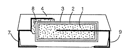
Fig. 24 shows a diagrammatic section through thf~ structure of
a conventional tantalum chip capacitor, while Fig. 25 shows a
io side view of the anode body of this chip capacitor and Fig. 26
shows a plan view of the anode body.
This conventional chip capacitor comprises the anode body 1, a
dielectric 2 and a layered cathode 3, which ford an actual
i5 capacitor element.
In addition, there is a housing 4 which is responsible for
important protective functions for the capacitor. element.
2o A tantalum wire 5, which in the interior of the housing 4 is
connected to a first metal connector 6, leads to the capacitor
element comprising the anode body 1, the dielectric 2 and the
layered cathode 3. By means of a conductive adhesive 8, the
layered cathode 3 is connected to a second metal. connector 7
25 which, like the metal connector 6, leads out of the housing 4.
Chip capacitors of this nature are produced in different sizes
of housing 4, usually with standardized basic surface area
dimensions and structural heights. Consequently, to achieve a
3o higher CV product, the volume taken up by the capacitor
element or the anode body 1 contained therein ha.s to be
increased.
-2-
CA 02379305 2002-O1-15
Owing to the use of the tantalum wire 5 in the dynode body 1
(cf. in this respect in particular Figs. 25 and 26) as the
anode-side conductor, the utilization of the housing can
scarcely be increased further. This is because t:he free end of
s the tantalum wire 5 is welded to the metal connector 6 which,
in the finished chip capacitor, is intended to provide
electrical connection to an electronic circuit on a printed-
circuit board, together with the other metal connector. In a
design of this nature, the distance between the capacitor
io element and the housing wall is particularly great especially
on the positive side. The distance between the positive metal
connector 6 and the capacitor element or the anode body 1,
which is formed by the tantalum wire 5, can scarcely be
reduced further, for manufacturing reasons. In other words, in
i5 the known chip capacitor the volume of the housing is only
insufficiently utilized.
Patent DD 215 420 has disclosed a tantalum chip capacitor in
which an anode conductor is embedded in a two-part anode body
2o produced by extrusion. Then, the anode body is ~~intered to the
anode conductor. The use of two pre-extruded partial anode
bodies has the drawback that it is impossible to achieve an
exact form fit between the anode body and the anode conductor,
owing to manufacturing tolerances. Consequently, the
2s electrical contact between anode body and anode conductor is
impaired.
Furthermore, document DE 36 34 103 A1 has disclosed a tantalum
capacitor in which a tantalum powder is pressed around a wire
3o anode conductor. This capacitor has the drawback of a small
contact area between the wire anode conductor arid the anode
body. The result is an increased resistance in t:he capacitor
which may have an adverse effect on the electrical
-3-
CA 02379305 2002-O1-15
characteristics of the capacitor. This is an undesirable
effect.
Furthermore, document US 3,903,589 has disclosed a tantalum
s capacitor, the anode of which is produced by immersing the
anode conductor in a dispersion containing metal powder. When
the anode conductor is pulled out of the dispersion, a drop
remains hanging from the anode conductor, which is then dried
and sintered. This tantalum capacitor has the d:=awback that
to the anode body cannot be produced with a defined geometry.
Because of the absence of an optimized anode geometry and the
broad tolerances, the known capacitor exhibits poor volume
utilization.
15 Therefore, the object of the present invention :is to specify
an anode which has a large contact area between the anode
conductor and the anode body, the anode body of which is of
fixedly predetermined shape and in which there :is good
electrical contact between the anode body and the anode
2o conductor.
The invention provides an anode for an electrol~rtic capacitor,
having an anode body of fixedly predetermined shape and having
a flat anode conductor, in which the anode body is molded onto
25 the anode conductor from a continuously deformable material
which can be solidified.
Furthermore, the invention provides a capacitor in which the
anode body is surrounded by a dielectric, in which a layered
3o cathode is provided on tie dielectric, in which a further end
section of the anode conductor is shaped into a first terminal
connector and in which the layered cathode is connected to a
second terminal connector.
-4-
CA 02379305 2002-O1-15
The anode according to the invention has the ad,~antage that as
a result of the entire anode body being molded onto the anode
conductor in the form of a continuously deformable material,
it is possible to form a homogeneous anode body which exhibits
s a good form fit with the anode conductor and good electrical
contact with the anode conductor.
Furthermore, the anode according to the invention has the
advantage that, as a result of the anode body being shaped
to with the aid of a continuously deformable material, it is
possible to achieve any desired shape with the aid of suitable
molds which are removed before or after solidification of the
anode body. The material from which the anode body is formed
may, for example, be a paste containing metal powder, a green
15 film produced from the paste, or a suitable met<~1 powder
itself.
Due to the flat design of the anode conductor which is
sintered into the anode body made from sintered tantalum
2o powder, for example, a larger contact area between anode
conductor and anode body is achieved compared wuth a sintered-
in tantalum wire of the same cross-sectional area. The number
of powder particles which are in contact with the surface of
the anode conductor is increased, and consequently the mean
25 length of the current paths between the dielectric and the
anode conductor, which comprise tantalum partic=_es which have
been sintered together, is reduced. Consequentl3r, it is
possible to achieve reduced resistances and an :_ncreased
capacitance at high frequencies.
Moreover, the use of a flat anode conductor in t:he anode body
reduces the risk of local overheating at the tr~insitions
between the anode conductor and a fine network formed by the
sintered tantalum particles when current is flovaing. This is
-5-
CA 02379305 2002-O1-15
because higher current densities occur at these transitions
than in the adjoining network. Local overheatin<~ of this type
may be a cause of chip capacitors being suddenl=~ and
dramatically eroded.
The essential feature of the capacitor or anode according to
the invention is in particular the production o:E a strong,
large-area connection between the anode body, comprising an
open-pored sintered body which forms the capacitance, and an
to anode conductor with a large surface area. For <~11 these
components, it is preferable to use tantalum or another
suitable metal, such as niobium or a material which allows a
layer with a high dielectric constant to be formed.
i5 Furthermore, an anode in which the anode body completely
surrounds an end section of the anode conductor is
advantageous. In this way, it is possible to achieve optimum
utilization or the surface area of the anode conductor for
contact with the anode body. Furthermore, high mechanical
2o stability of the anode is ensured in this way.
Furthermore, the invention provides a process for producing
the anode according to the invention, in which ~~ continuously
deformable material, which can be solidified, i:~ molded onto a
25 flat anode conductor with simultaneous external shaping, and
is then solidified to form an anode body. The simultaneous
molding of the material onto the anode conductor_ and the
defining of the external shape of the anode bod~r with the aid
of a continuously deformable material obviates t;he need for
3o complex post-machining processes for shaping the' anode body.
A process in which a paste which contains a binder system and
a powder is applied to the anode conductor and is then dried
and sintered is particularly advantageous. In this process,
-6-
CA 02379305 2002-O1-15
the paste may be combined with the anode conduct=or to form an
anode by means of various methods. By way of example, it is
possible to use a paste which is known from document DE 199 27
909 A1 and which comprises a discrete phase coni~aining a metal
powder and a continuous phase containing organic. compounds.
The capacitor according to the invention can be used as an SMD
(SMD = Surface Mounted Device). The use of a paste simplifies
the processing of high capacitance and ultra-high capacitance
to tantalum powders.
Furthermore, the invention provides a process for producing
the anode according to the invention, in which a powder is
pressed around a flat anode conductor, with the anode
conductor projecting on one side. Then, the compact is
sintered. The process according to the invention may
advantageously be carried out in such a way that: an anode
conductor in the form of a strip-like metal sheEet is pushed
into a bed of the powder which is situated in a press mold,
2o and then the pressing operation takes place.
The material tantalum which is preferably used f:or the anode
conductor is extremely expensive, and consequently the strip
used for the process should be as thin as possible.
Conversely, the tantalum sheet used must be sufficiently
mechanically stable to be able to be pushed intc> the powder
bed and subsequently bent into a mechanically stable
connector. Within these boundary conditions, strip-like anode
conductors with a width of between 0.3 and 5 mm and a
3o thickness of between 50 and 150 ~m have proven ~,uitable. These
anode conductors have a width/thickness ratio of between 2 and
100.
CA 02379305 2002-O1-15
The pressing of the powder may particularly advantageously be
carried out by transverse pressing, that is to ;gay by pressing
transversely with respect to the direction in which the strip-
like anode conductor extends.
The further manufacturing steps correspond to the steps used
for the conventional manufacture of tantalum chap capacitors.
Therefore, in the procedure known as forming, the dielectric
is formed from tantalum pentoxide on the inner and outer
io surfaces of the sintered anode body. After the cathode layers
have been applied, cathode terminal and housing are produced.
In the configuration according to the invention; the anode
connector made from tantalum, which is used as t:he positive
electrical terminal, may undergo further treatment in order to
be made suitable for soldering or adhesive bond_~ng, and this
statement also applies to the other exemplary embodiments.
As a modification to the above design according to the
invention of the tantalum chip capacitor, the tantalum powder
2o is also mixed with an additive which, due to it:~ lubricating
action, makes the pressing operation easier and more gentle on
the press mold. The flow properties of the powder and the
mechanical stability of the compact are also improved by the
binding action of the additive. Camphor is a st~indard
additive. Before the compact is sintered, the additive should
be removed as far as possible without leaving any residues.
As an alternative to tantalum, it is also possible to use
other suitable metals, such as for example niobium, or alloys
of suitable metals, or other materials which are' capable of
forming a dielectric.
The invention is explained in more detail below with reference
to the drawings, in which:
-g_
CA 02379305 2002-O1-15
Figs. 1 to 3 show diagrammatic illustrations explaining a
first exemplary embodiment of the invention,
Figs. 4 to 6 show diagrammatic illustr~.tions
explaining a second exemplary embodiment of the invention,
Figs. 7 to 13 show diagrammatic illustrations
explaining a first process for producing an anode body,
to
Figs. 14 and 15 show diagrammatic illustrations explaining a
modification of the process shown in Figs. 7 to 13,
Figs. 16 to 23 show diagrammatic illustrations explaining a
second process for producing an anode body and
Figs. 24 to 26 show diagrammatic illustrations a~xplaining a
conventional chip capacitor.
2o Figs. 24 to 26 have already been described in the
introduction. In the figures, corresponding components are in
each case provided with identical reference numESrals.
Fig. 1 shows a chip capacitor according to the invention,
2s having an actual capacitor element comprising an anode body 1,
a dielectric 2, a layered cathode 3 and a flat <anode conductor
9 which extends into the anode body 1. The anods~ body 1
comprises a porous sintered metal body which, a:~ will be
explained in more detail below, is constructed :=rom a paste
3o which contains metal powder and is dried and sintered, in the
process forming a firm, large-area connection to the anode
conductor 9.
_g_
CA 02379305 2002-O1-15
The anode conductor 9 is preferably made from t,~ntalum, which
is advantageously also used as the metal for th~= metal powder
in the paste.
As in the conventional chip capacitor shown in :Fig. 24 the
layered cathode 3 is connected to the metal con:~ector 7 via a
conductive adhesive 8.
The anode conductor 9 fulfills the functions of the tantalum
to wire 5 and the metal connector 6 in the conventional chip
capacitor shown in Fig. 24: for this purpose, it is bent or
shaped into a contact connector (cf. in particular Figs. 2 and
3), with the result that the distance between the capacitor
element and the edge of the housing 4 on the po;~itive side can
be reduced. Consequently, the volume of the hou;~ing 4 of the
component is better utilized, in order advantageously to
achieve a higher CV product. Thus, it is possib:Le to select a
smaller size of housing 4, while the volume of the anode body
1 remains constant. If the size of housing 4 remains the same,
2o the invention allows the capacitor element or the anode body 1
to be larger than in the prior art shown in Fig;. 24 to 26.
The chip capacitor according to the invention having the flat
anode conductor 9 in the anode body 1 makes it possible to
produce extremely shallow capacitor elements, a:~ can be seen
diagrammatically in Figs. 4 to 6. Fig. 5, like l~ig. 2, shows a
side view of the anode body 1 with the anode conductor 9,
while Fig. 6, like Fig. 3, shows a plan view of the anode body
1 with the anode conductor 9. However, Figs. 3 <~nd 6 show the
3o entire extent of the anode conductor 9, even though it is in
fact partially covered by the anode body 1.
The shallow design, in accordance with the exemplary
embodiment shown in Figs. 4 to 6, results in a particularly
-10-
CA 02379305 2002-O1-15
large lateral surface area, which allows short ~~urrent paths
and improves the electrical properties. If appr~~priate, the
extremely shallow capacitor elements may also b~~ integrated in
hybrid circuits without housings.
To produce an anode body, a paste comprising a hinder system
and a tantalum powder is printed onto a tantalum foil or a
tantalum sheet 10 with a thickness of from 50 to 150 Vim, using
a stencil 11. Fig. 7 shows a plan view of this ;stencil 11,
to while Fig. 8 shows a side view of the tantalum :sheet 10,
together with the stencil 11, and Fig. 9 shows i~he stencil 11
once it has been filled with tantalum paste 12. The tantalum
sheet 10 together with the tantalum paste 12 which has been
doctored or printed on, is dried and sintered following
removal of the stencil 11, so that the arrangement shown in
side view in Fig. 10 is obtained.
Finally, the arrangement shown in Fig. 10 is cut: to length
along the dotted lines (cf. Fig. 11), so that the result is
2o anode bodies which are connected to the tantalum sheet 10.
Fig. 12 shows a side view of an anode body of this type with a
tantalum sheet 10, while Fig. 13 shows a plan view thereof.
If appropriate, the cutting to length to form tree individual
anode bodies (cf. Fig 11), given sufficient drying, may also
take place prior to sintering.
The subsequent process steps correspond to thosE~ used for the
conventional manufacture of tantalum chip capacitors. Thus, in
3o a procedure known as forming, the dielectric 2 is formed from
tantalum pentoxide on the inner and outer surfaces of the
sintered anode body 1. After the layered cathode: 3 has been
applied, the cathode terminal or metal connector 7 and housing
4 are produced. The anode connector made from tr.e anode
-11-
CA 02379305 2002-O1-15
conductor 9 made from tantalum, which serves as the positive
electrical terminal, may be treated further for the purpose of
making it more suitable for soldering or adhesive bonding.
As a modification to the exemplary embodiment shown in Figs. 7
to 13, it is possible for the tantalum paste 12 to be printed
onto the tantalum sheet 10 on both sides, which may take place
in a single operation. For printing in two steps, after the
first side of the tantalum sheet 10 has been printed, the
to paste which has been applied to this side under<~oes
preliminary drying. Irrespective of whether the printing is
carried out in one operation or in two operations, the
ultimate result is an arrangement as shown in Figs. 14 and 15,
Fig. 14 showing a side view while Fig. 15 shows a plan view of
the tantalum sheet 10 with the anode body comprising two
parts.
The anode body for the chip capacitor can also be produced by
screen-printing, for which purpose a paste comp;=ising a binder
2o system and tantalum powder is screen-printed onto a tantalum
foil or a tantalum sheet 10 with a thickness of from 50 to 150
Vim. As in the previous examples, the tantalum sheet 10 with
the screen-printed tantalum paste 12 is dried and sintered.
Following sintering, the tantalum sheet 10 is cut to length.
In this way, individual anode bodies with an anode conductor
comprising tantalum sheet 10 or tantalum foil corresponding to
those shown in Figs. 12 and 13 are obtained. In this case too,
the cutting to length, given sufficient drying, may also take
3o place prior to the actual sintering.
The further process steps are carried out in the manner
explained above.
-12-
CA 02379305 2002-O1-15
It is also possible to screen-print onto the tantalum sheet 10
on both sides, if appropriate, in one operation. If the
printing is carried out in two steps, after the paste has been
printed on the first side of the tantalum sheet 10,
preliminary drying may be carried out. In this ~~ay, the
ultimate result is the arrangement shown in Figs. 14 and 15,
having the tantalum sheet 10 and the tantalum p,~stes 12 which
have been sintered, to form anode bodies.
to In an exemplary embodiment of the invention whi~~h is explained
with reference to Figs. 16 to 23, an anode conductor is
completely enclosed by a metal powder paste, so that the anode
conductor can only project out of an anode body 20 produced
from the metal powder paste by drying and sintering on one
i5 side, as is shown first of all in a side view azd plan view in
Figs. 22 and 23, respectively. To produce an arrangement of
this nature, it is possible to employ a multist~~ge stencil
process in which initially strips 15 of tantalum foil or
tantalum sheet with a thickness of from 50 to 1!~0 ~m are
2o placed between two perforated masks 13, 14. Fig. 16 shows a
plan view of the perforated mask 13, together with the strips
15, while Fig. 17 shows a side view of the perforated masks
13, 14 together with the strips 15 on a first base plate 16.
That part of the strip 15 which projects into the hole in the
25 perforated masks 13, 14 may be supported by a s~~acer 17 (cf.
Fig. 17). If appropriate, this spacer 17 may al:~o be part of
the base plate 16 or may be fixed thereto.
After preliminary drying of a paste 18 which ha;~ been doctored
3o in (cf. Fig. 18), a further base plate 19 is fitted (cf. Fig.
19), the first base plate 16 together with the :pacers 17 is
removed (cf. Fig. 20), and metal powder paste i:~ doctored in a
second time (cf. Fig. 21). Following final shaping, drying and
sintering are carried out. In this way, it is p«ssible to
-13-
CA 02379305 2002-O1-15
obtain the arrangements shown in Figs. 22 and 23 with the
anode body 20.
Alternatively, to produce a chip capacitor, it is also
possible for a paste comprising a binder system and a tantalum
powder to be injected, pressed or cast around a strip of
tantalum foil or tantalum sheet with a thickness of from 50 to
150 Vim. Following final shaping, the anode body obtained in
this way is dried and sintered. In this way, individual anode
to bodies with an anode conductor made from tantalum foil or
tantalum sheet corresponding to Fig. 22 (side view) and Fig.
23 (plan view) are obtained, and these anode bodies are
treated further in the manner explained above.
As a final option for producing an anode body, it is also
possible for an elastic, film-like mass (green film) to be
prefabricated from a paste which comprises a binder system and
tantalum powder, and this mass is then cut to length and
adhesively bonded to the tantalum foil or the tantalum sheet
2o with a thickness of from 50 to 150 Vim. Following drying and
sintering, individual anode bodies with an anode conductor
made from tantalum foil or tantalum sheet are obtained, as
illustrated in Figs. 22 and 23.
The anode bodies which are produced by the pressing process
using powder which is described above look exactly like those
illustrated in Figs. 22 and 23.
-14-