Note: Descriptions are shown in the official language in which they were submitted.
CA 02397806 2002-07-19
WO 01/53113 PCT/US00/27999
1
OPTICALLY VA.RIASLE SECURITY DEVICES
BACKGROUND OF THE INVENTION
1. The Field of the Invention
The present invention is related generally to thin film optical coatings for
use in
producing security articles. More specifically, the present invention is
related to the
production of diffractive surfaces such as holograms or gratings having color
shifting or
optically variable backgrounds which can be used as security articles in a
variety of
applications.
2. The Relevant Technology
Color shifting pigments and colorants have been used in numerous applications,
ranging fiom automobile paints to anti-counterfeiting inks for security
documents and
currency. Such pigments and colorants exhibit the property of changing color
upon
variation of the angle of incident light, or as the viewing angle of the
observer is shifted.
The primary method used to achieve such color shifting colorants is to
disperse small
flakes, which are typically composed of multiple layers of thin fihns having
particular
optical characteristics, throughout a medium such as paint or ink that may
then be
subsequently applied to the surface of an object.
Diffraction patterns and embossments, and the related field of holographs,
have
begun to find wide-ranging practical applications due to their aesthetic and
utilitarian
visual effects. One very desirable decorative effect is the iridescent visual
effect created
by a diffraction grating. This striking visual effect occurs when ambient
light is
diffiacted into its color components by reflection from the diffraction
grating. In general,
diffraction gratings are essentially repetitive structures made of lines or
grooves in a
material to form a peak and trough structure. Desired optical effects within
the visible
spectrum occur when diffraction gratings have regularly spaced grooves in the
range of
hundreds to thousands of lines per millimeter on a reflective surface.
Diffraction grating technology has been employed in the fonmation of two-
dimensional holographic patterns which create the illusion of a three-
dimensional image
to an observer. Three-dimensional holograms have also been developed based on
differences in refractive indices in a polymer using crossed laser beams,
including one
reference beam and one object beam. Such holograms are called volume holograms
or
3D holograms. Furthermore, the use of holographic images on various objects to
discourage counterfeiting has found widespread application.
CA 02397806 2002-07-19
WO 01/53113 PCT/US00/27999
2
There currently exist several applications for surfaces embossed with
holographic
patterns which range from decorative packaging such as gift wrap, to security
documents
such as bank notes and credit cards. Two-dimensional holograms typically
utilize
diffraction patterns which have been formed on a plastic surface. In some
cases, a
holographic image which has been embossed on such a surface can be visible
without
further processing; however, it is generally necessary, in order to achieve
maximum
optical effects, to place a reflective layer, typically a thin metal layer
such as aluminum,
onto the embossed surface. The reflective layer substantially increases the
visibility of
the diffraction pattern embossment.
Every type of first order diffraction structure, including conventional
holograms
and grating images, has a major shortcoming even if encapsulated in a rigid
plastic.
When diffuse light sources, such as ordinary room lights or an overcast sky,
are used to
illuminate the holographic image, all diffraction orders expand and overlap so
that the
diffraction colors are lost and not much of the visual information contained
in the
hologram is revealed. What is typically seen is only a silver colored
reflection from the
embossed surface and all such devices look silvery or pastel, at best, under
such viewing
conditions. Thus, holographic images generally require direct specular
illumination in
order to be visualized. This means that for best viewing results, the
illuminating light
must be incident at the same angle as the viewing angle.
Since the use of security holograms has found widespread application, there
exists
a substantial incentive for counterfeiters to reproduce holograms which are
frequently
used in credit cards, banknotes, and the hke. Thus, a hurdle that security
holograms must
overcome to be truly secure, is the ease at which such holograms can be
counterfeited.
One step and two step optical copying, direct mechanical copying and even re-
origination
have been extensively discussed over the Internet. Various ways to counteract
these
methods have been explored but none of the countermeasures, taken alone, has
been
found to be an effective deterrent.
One of the methods used to reproduce holograms is to scan a laser beam across
the embossed surface and optically record the reflected beam on a layer of a
material such
as a photopolymerizable polymer. The original pattern can subsequently be
reproduced
as a counterfeit. Another method is to remove the protective covering material
from the
embossed metal surface by ion etching, and then when the embossed metal
surface is
exposed, a layer of metal such as silver (or any other easily releasable
layer) can be
deposited. This is followed by deposition of a layer of nickel, which is
subsequently
released to form a counterfeiting embossing shim.
CA 02397806 2002-07-19
WO 01/53113 PCT/US00/27999
3
Due to the level of sophistication of counterfeiting methods, it has become
necessary to develop more advanced security measures. One approach, disclosed
in U.S.
Patent Nos. 5,624,076 and 5,672,410 to Miekka et al., embossed metal particles
or optical
stack flakes are used to produce a holographic image pattern.
A further problem with security holograms is that it is difficult for most
people
to identify and recollect the respective images produced by such holograms for
verification purposes. The ability of the average person to authenticate a
security
hologram conclusively is compromised by the complexity of its features and by
confusion
with decorative diffractive packaging. Thus, most people tend to confnm the
presence
of such a security device rather than verifying the actual image. This
provides the
opportunity for the use of poor counterfeits or the substitution of commercial
holograms
for the genuine security hologram.
In other efforts to thwart counterfeiters, the hologram industry has resorted
to
more complex images such as producing multiple images as the security device
is rotated.
These enhanced images provide the observer with a high level of "flash" or
aesthetic
appeal. Unfortunately, this added complexity does not confer added security
because this
complex imagery is hard to conununicate and recollection of such imagery is
difficult,
if not impossible, to remember.
It would therefore be of substantial advantage to develop iinproved security
products which provide enhanced viewing qualities in various lighting
conditions,
especially in diffuse lighting, and which are usable in various security
applications to
make counterfeiting more difficult.
SUMMARY OF THE INVENTION
In accordance with the invention as embodied and broadly described herein, a
security article is provided which includes a light transmissive substrate
having a first
surface and an opposing second surface, with the first surface having an
optical
interference pattern such as a holographic image pattern or an optical
diffraction pattern
thereon. A color shifting optical coating is formed on the substrate such as
on the
interference pattern or on the opposing second surface of the substrate, with
the optical
coating providing an observable color shift as the angle of incident light or
viewing angle
changes. Various processes can be utilized to form the security article, such
as vacuum
coating processes, organic coatings, lamination, laser scribing, and laser
imaging.
The color shifting optical coating can be varied in different embodiments of
the
invention. For example, the optical coating can be a multilayer optical
interference film
CA 02397806 2002-07-19
WO 01/53113 PCT/US00/27999
4
such as a three layer optical stack of absorber-dielectric-reflector, or
altemating layers of
low and high index of refraction dielectric layers. In addition, the optical
coating can be
formed from a plurality of multilayer optical interference flakes dispersed in
a polymeric
medium such as a color shifting ink.
In other embodiments, various security articles are formed by lami.nating a
prelaminate structure including a color shifting optical coating, which can
optionally be
laser imaged by ablation, to a substrate embossed with an optical interference
pattern.
In another method of the invention, a color shifting optical coating is formed
on
a master shim so as to conform to the shape of an optical interference pattern
on the shim.
A carrier substrate layer is affixed to the optical coating and is removed
along with the
optical coating from the shim to produce a security article with the
interference pattern
replicated in the optical coating.
The security article of the invention can be affixed to a variety of objects
through
various attachment mechanisms, such as pressure sensitive adhesives or hot
stamping
processes, to provide for enhanced security measures such as
anticounterfeiting. The
security article can be utilized in the form of a label, a tag, a ribbon, a
security thread, and
the like, for application to a variety of objects such as security documents,
monetary
currency, credit cards, merchandise, etc.
These and other aspects and features of the present invention will become more
fully apparent from the following description and appended claims, or may be
learned by
the practice of the invention as set forth hereinafter.
BRIEF DESCRIPTION OF THE DRAWINGS
In order to more fully understand the manner in which the above-recited and
other
advantages and objects of the invention are obtained, a more particular
description of the
invention will be rendered by reference to specific embodiments thereof which
are
illustrated in the appended drawings. Understanding that these drawings depict
only
typical embodiments of the invention and are not therefore to be considered as
limiting
of its scope, the invention will be described and explained with additional
specificity and
detail through the use of accompanying drawings in which:
Figure 1 is a schematic depiction of a security article according to one
embodiment of the present invention;
Figure 2 is a schematic depiction of a security article according to another
embodiment of the present invention;
CA 02397806 2002-07-19
WO 01/53113 PCT/US00/27999
Figure 3 is a schematic depiction of a security article according to a further
embodiment of the present invention;
Figure 4 is a schematic depiction of a security article according to another
embodiment of the present invention;
5 Figure 5 is a schematic depiction of a security article according to yet
another
embodiment of the present invention;
Figure 6 is a schematic depiction of a security article according to a further
embodiment of the present invention;
Figure 7 is a schematic depiction of a security according to another
embodiment
of the present invention;
Figure 8A is a scheniatic depiction of a security article according to a
fiuther
embodiment of the present invention;
Figure 8B is an enlarged sectional view of the security article of Figure 8A;
Figure 9 is a schematic depiction of a security article according to another
embodiment of the present invention;
Figure l0A is a schematic depiction of a prelaminate structure used to form a
security article according to an additional embodiment of the present
invention;
Figure lOB is a schematic depiction of a security article formed from the
prelanvnate structure of Figure 10A;
Figure 11 is a schematic depiction of a security article according to another
embodiment of the present invention;
Figure 12 is a schematic depiction of a security article according to an
alternative
embodiment of the present invention;
Figure 13 is a schematic depiction of a security article according to an
additional
embodiment of the present invention;
Figure 14 is a schematic depiction of a security article according to another
embodiment of the present invention;
Figure 15 is a schematic depiction of a hot stamping process used to form one
embodiment of a security article according to the invention;
Figure 16 is a schematic depiction of a hot stamping process used to form
another
embodiment of a security article according to the invention;
Figures 17A and 17B are diagrams showing the geometries of various viewing
conditions used in measuring the optical characteristics of a security article
of the
invention;
CA 02397806 2002-07-19
WO 01/53113 PCT/US00/27999
6
Figure 18 is a graph showing the spectral profiles for a security article of
the
invention;
Figure 19 is a graphical representation of the CIE Lab color space showing
trajectory of color for a security article of the invention;
Figure 20 is a graph showing the off-gloss spectral profiles for a security
article
of the invention;
Figure 21 is a graph showing the on-gloss spectral profiles for a security
article
of the invention;
Figure 22 is a graph showing the on-gloss spectral profiles for a security
article
of the invention;
Figure 23 is a photomicrograph of a thin film optical stack used in a security
article of the invention; and
Figures 24A and 24B are photomicrographs showing holographic relief at the top
of a thin film optical stack used in a security article of the invention.
DETAILED DESCRIPTION OF THE 1NVENTION
The present invention is directed to security articles having diffractive
surfaces
with color shifting backgrounds that produce enhanced visual effects. The
confguration
of the security articles is such that a combination of optical interference
patterns such as
holographic or diffraction grating patterns with color shifting foils or inks
decreases the
possibility of counterfeiting. Furthermore, the articles of the invention
allow a user to
more easily view the image or diffraction effect in diffuse light without the
need for direct
specular light.
Generally, the configuration of the security articles of the present invention
is
such that the combination of a light transmissive substrate, having an
interference pattern
on the surface thereof, with color shifting optical coatings provides security
features that
make forgery or counterfeiting of an object difficult. The present invention
combines the
performance features of light interference effects with the diffractive
effects of a
dif&active surface such as a hologram. The security articles allow for ready
identification
by the average person while still preserving complex optical patterns, thus
overcoming
disadvantages of conventional holographic technology,
The various embodiments of the invention, described in further detail below,
can
be formed using three basic constructions. One involves substituting the
aluminum
reflector of a hologram or other diffractive surface with a thin film optical
interference
stack. This construction builds the hologram structure right into the optical
interference
CA 02397806 2002-07-19
WO 01/53113 PCT/US00/27999
7
stack. In this case, the optical coating is vacuum deposited directly onto the
embossed
surface. The second construction adds a thin film color shifting foil or ink
to the side of
a substrate opposite of the embossing. Whether foil or ink is used, the
interference effect
can be based on a metal-dielectric-absorber interference structure, or all-
dielectric optical
designs. The third approach involves laminating a color shifting optical
coating structure,
which can be digitally imaged by laser ablation, reflective pattern etching,
or chemical
etching by photolithography, to a diffractive surface such as a hologram.
Referring to the drawings, wherein li?ce structures are provided with like
reference
designations, Figure 1 depicts a security article 10 according to one
embodiment of the
present invention. The security article 10 includes a light transmissive
substrate 12
having an optical interference pattern 14 such as an embossed image on an
outer first
surface thereof. A color shifting optical coating 16 is formed on an opposing
second
surface of substrate 12 and is discussed in further detail below. The
combination of
substrate 12 and color shifting optical coating 16 forming security article 10
provides a
security feature that reduces the possibility of duplication, forgery and/or
counterfeiting
of an object having security article 10 thereon.
The optical interference pattern 14 formed on the outer surface of light
transmissive substrate 12 can take various conventional forms including
diffraction
patterns such as diffraction gratings, refraction patterns, holographic
patterns such as two-
dimensional and three-dimensional holographic images, corner cube reflectors,
Kinegram devices, Pixelgram devices, zero order diffraction patterns, moire
patterns,
or other light interference patterns based on microstructures having
dimensions in the
range from about 0.1 m to about l0 m, preferably about 0.l,um to about 1,um,
and
various combinations of the above such as hologram/grating ima.ges, or other
like
interference patterns.
The particular methods and structures that form optical interference pattern
14 are
known by those skilled in the art. For example, embossing the light
transmissive
substrate to form an interference pattern such as a hologram thereon can be
done by well
known methods, such as embossing the surface of a plastic film by pressing it
in contact
with a heated nickel embossing shim at high pressure. Other methods include
photolithography, molding of the plastic fihn against a patterned surface, and
the like.
The Kinegram device is a two-dimensional, computer-generated image
(available from OVD Kinegram Corp. of Switzerland) in which the individual
picture
elements are filled with light-diffracting microstructures. These
microstructures are
extremely fine surface modulations with typical dimensions of less than one
micrometer.
CA 02397806 2002-07-19
WO 01/53113 PCT/US00/27999
8
Generally, moldable thennoformable materials are used to form light
transmissive
substrate 12 and include, for example, plastics such as polyethylene
terephthalate (PET),
especially PET type G, polycarbonate, acrylics such as polyacrylates including
polymethyl methacrylate (PNIMA), polyacrylonitrile, polyvinyl chloride,
polystyrene,
cellulose diacetate and cellulose triacetate, polypropylene,
polydicyclopentadiene,
mixtures or copolymers thereof, and the like. In one preferred embodiment,
light
transmissive substrate 12 is substantially composed of a transparent material
such as
polycarbonate. The substrate 12 is formed to have a suitable thickness of
about 3 m to
about 100 m, and preferably a thickness of about 12 m to about 25 m. In
addition,
substrate 12 can be made of one layer or multiple layers of substrate
materials.
Generally, substrate 12 should have a lower melting point or glass transition
temperature
than the optical coating, while being transparent.
In one method, substrate 12 can be produced from a thermoplastic film that has
been embossed by heat softening the surface of the film and then passing the
film through
embossing rollers which impart the diffraction grating or holographic image
onto the
softened surface. In this way, sheets of effectively unlimited length can be
formed with
the diffraction grating or holographic image thereon. Alternatively, the
diffractive
surface can be made by passing a roll of plastic fi1m coated with an
ultraviolet (UV)
curable polymer, such as P1VIIVIA, through a set of UV transparent rollers
whereby the
rollers set a diffractive surface into the UV curable polymer and the polymer
is cured by
a UV light that passes through the UV transparent rollers.
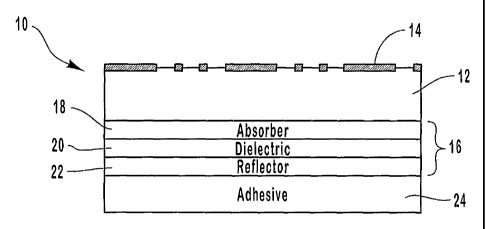
As shown in Figure 1, the color shifting optical coating 16 is a multilayer
optical
interference stack or foil that includes an absorber layer 18, a dielectric
layer 20, and a
reflector layer 22. The absorber layer 18 can be deposited on light
transmissive substrate
12 by a conventional deposition process such as physical vapor deposition
(PVD),
sputtering, or the like. The absorber layer 18 is formed to have a suitable
thickness of
about 30-300 A Angstroms (A), and preferably a thickness of about 50-100 A.
The absorber layer 18 can be composed of a semi-opaque material such as a grey
metal, including metals such as chromium, nickel, titanium, vanadium, cobalt,
and
palladium, as well as other metals such as iron, tungsten, molybdenum,
niobium,
aluminum, and the like. Various combinations and alloys of the above metals
may also
be utilized, such as Inconel (Ni-Cr-Fe). Other absorber materials may also be
employed
in absorber layer 18 including metal compounds such as metal sub-oxides, metal
sulfides,
metal nitrides, metal carbides, metal phosphides, metal selenides, metal
silicides, and
CA 02397806 2002-07-19
WO 01/53113 PCT/US00/27999
9
combinations thereof, as well as carbon, germanium, ferric oxide, metals mixed
in a
dielectric matrix, and the like.
The dielectric layer 20 can be formed on absorber layer 18 by a conventional
deposition process such as PVD, chemical vapor deposition (CVD), plasma
enhanced
chemical vapor deposition (PECVD), reactive DC sputtering, RF sputtering, or
the like.
The dielectric layer 20 is formed to have an effective optical thickness for
imparting color
shifting properties to security article 10. The optical thickness is a well
known optical
parameter defined as the product r7d, where 77 is the refractive index of the
layer and d
is the physical thickness of the layer. Typically, the optical thickness of a
layer is
expressed in terms of a quarter wave optical thickness (QWOT) that is equal to
4 rjdl2,
where .l is the wavelength at which a QWOT condition occurs. The optical
thickness of
dielectric layer 20 can range from about 2 QWOT at a design wavelength of
about 400
nm to about 9 QWOT at a design wavelength of about 700 nm, and preferably 2-6
QWOT at 400-700 nm, depending upon the color shift desired. Suitable materials
for
dielectric layer 20 include those having a "high" index of refraction, defined
herein as
greater than about 1.65, as well as those have a "low" index of refraction,
which is
defined herein as about 1.65 or less.
, Examples of suitable high refractive index materials for dielectric layer 20
include
zinc sulfide (ZnS), zinc oxide (ZnO), zirconium oxide (Zr02)1 titanium dioxide
(Ti0z),
carbon (C), indium oxide (In203), indium-tin-oxide (ITO), tantalum pentoxide
(Ta205),
ceric oxide (CeO2)1 yttrium oxide (Y203), europium oxide (Eu203), iron oxides
such as
(II)diiron(III) oxide (Fe304) and ferric oxide (Fe203), hafnium nitride (HfN),
hafnium
carbide (HfC), hafnium oxide (HfOz)1 lanthanum oxide (La203)1 magnesium oxide
(MgO), neodymium oxide (Nd203), praseodymium oxide (Pr6011), samarium oxide
(Sm203), antimony trioxide (Sbz03), silicon carbide (SiC), silicon nitride
(Si3N4), silicon
monoxide (SiO), selenium trioxide (Se203), tin oxide (SnOz)1 tungsten trioxide
(W03),
combinations thereof, and the like.
Suitable low refractive index materials for dielectric layer 20 include
silicon
dioxide (Si02), aluminum oxide (A1203), metal fluorides such as magnesium
fluoride
(MgF2), aluminum fluoride (AlF3), cerium fluoride (CeF3), lanthanum fluoride
(LaF3),
sodium aluminum fluorides (e.g., Na3AlF6 or NasA13F14), neodymium fluoride
(NdF3),
samarium fluoride (SmF3), barium fluoride (BaF2), calcium fluoride (CaF2),
lithium
fluoride (LiF), combinations thereof, or any other low index material having
an index of
refraction of about 1.65 or less. For example, organic monomers and polymers
can be
utilized as low index materials, including dienes or alkenes such as acrylates
(e.g.,
CA 02397806 2002-07-19
WO 01/53113 PCT/US00/27999
methacrylate), perfluoroalkenes, polytetrafluoroethylene (Teflon), fluorinated
ethylene
propylene (FEP), combinations thereof, and the like.
The reflector layer 22 can be formed on dielectric layer 20 by a conventional
deposition process such as PVD, sputtering, or the like. The reflector layer
22 is formed
5 to have a suitable thickness of about 300-1000 A, and preferably a thickness
of about
500-1000 A. The reflector layer 22 is preferably composed of an opaque, highly
reflective metal such as aluminum, silver, copper, gold, platinum, niobium,
tin,
combinations and alloys thereof, and the like, depending on the color effects
desired. It
should be appreciated that semi-opaque metals such as grey metals become
opaque at
10 approxiina.tely 350-400 A. Thus, metals such as chromium, nickel, titanium,
vanadium,
cobalt, and palladium, or cobalt-nickel alloys, could also be used at an
appropriate
thickness for reflector layer 22.
In addition, reflector layer 22 can be composed of a magnetic material such as
a
cobalt-nickel alloy, or can be formed of a semitransparent material, to
provide for
machine readability for security verification. For example, machine readable
information
may be placed on a backing underlying the optical coating, such as personal
identification numbers (PINS), account information, business identification of
source,
warranty information, or the like. In an alternative embodiment, reflector
layer 22 can
be segmented to allow for partial viewing of underlying information either
visually or
through the use of various optical, electronic, magnetic, or other detector
devices. This
allows for detection of information below optical coating 16, except in those
locations
where reflector segments are located, thereby enhancing the difficulty in
producing
counterfeits. Additionally, since the reflector layer is segmented in a
controlled manner,
the specific information prevented from being read is. controlled, providi.ng
enhanced
protection from forgery or alteration.
As shown in Figure 1, security article 10 can also optionally include an
adhesive
layer 24 such as a pressure sensitive adhesive on reflector layer 22. The
adhesive layer
24 allows security article 10 to be easily attached to a variety of objects
such as credit
cards, certificates of authenticity, bank cards, banknotes, visas, passports,
driver licenses,
immigration cards, and identification cards, as well as containers and other
three-
dimensional objects. The adhesive layer 24 can be composed of a variety of
adhesive
materials such as acrylic-based polymers, and p6lymers based on ethylene vinyl
acetate,
polyamides, urethane, polyisobutylene, polybutadiene, plasticized rubbers,
combinations
thereof, and the like. Alternatively, a hot stamping process, examples of
which are
discussed in further detail below, can be utilized to attach security article
10 to an object.
,
CA 02397806 2007-09-12
Doc. No.: 18-34 CA/PCT Patent
11
By using an absorber/dielectric/reflector design for color shifting optical
coating 16,
such as shown in Figurel, high chroma variable color effects are achieved that
are noticeable
to the human eye. Thus, an object having security article 10 applied thereto
will change color
depending upon variations in the viewing angle or the angle of the object
relative to the
viewing eye, as well as variations in angles of incident light. As a result,
the variation in colors
with viewing angle increases the difficulty to forge or counterfeit security
article 10.
Furthermore, the thin film interference color shifting coating changes the
diffractive colors,
either suppressing, modifying or enhancing certain colors depending on the
inherent color
shifts of the diffractive and thin film structures. By way of example, the
color-shifts that can
be achieved utilizing color shifting optical coating 16 in accordance with the
present invention
include, but are not limited to, gold-to-green, green-to-magenta, blue-to-red,
green-to-silver,
magenta-to-silver, magenta-to-gold, etc.
The color shifting properties of optical coating 16 can be controlled through
proper
design of the layers thereof. Desired effects can be achieved through the
variation of
parameters such as thickness of the layers and the index of refraction of each
layer. The
changes in perceived color which occur for different viewing angles or angles
of incident light
are a result of a combination of selective absorption of the materials
comprising the layers and
wavelength dependent interference effects. The interference effects, which
arise from the
superposition of the light waves that have undergone multiple reflections and
transmissions
within the multilayered structure, are responsible for the shifts in perceived
color with
different angles.
Figure 2 depicts a security article 30 according to another embodiment of the
present
invention. The security article 30 includes elements similar to those
discussed above with
respect to security article 10, including a light transmissive substrate 12
formed with an optical
interference pattern 14 on an outer first surface thereof, and a color
shifting optical coating 16
formed on an opposing second surface of substrate 12. The optical coating36 is
a multilayer
film that includes an absorber layer 18, a dielectric layer 20 thereon, and
another absorber
layer 38, but does not include a reflector layer. This multilayer film
configuration is disclosed
in U. S. Patent No. 5,278,590 to Phillips et al. Such a film structure allows
optical coating 36
to be transparent to light incident upon the surface thereof, thereby
providing for visual
verification or machine readability of information below optical coating 36 on
a carrier
substrate (not shown). An adhesive layer 24 such as a pressure sensitive
adhesive can be
optionally formed on absorber layer38 if desired to allow attachment of
security article 30 to
an appropriate surface of an object.
CA 02397806 2007-09-12
Doc. No.: 18-34 CA/PCT Patent
12
Figure 3 depicts a security article 40 according to a further embodiment of
the present
invention. The security article 40 includes elements similar to those
discussed above with
respect to security article 10, including a light transmissive substrate 12
formed with an optical
interference pattern 14 on an outer first surface thereof, and a color
shifting optical coating 46
formed on an opposing second surface of substrate 12. The optical coating 46
however, is a
multilayer optical stack that includes all dielectric layers. Suitable optical
stacks for optical
coating 46 that include all dielectric layers are disclosed in U. S. Patent
Nos. 5,135,812 and
5,084,351 to Phillips et al. Generally, optical coating 46 includes
alternating layers of low and
high index of refraction dielectric layers which can be composed of various
materials such as
those discussed above for dielectric layer 20. The all dielectric stack of
optical coating 46
enables security article 40 to be transparent to light incident upon the
surface thereof. An
adhesive layer 24 such as a pressure sensitive adhesive can be formed on
optical coating 46 if
desired.
Figure 4 depicts a security article 50 according to a further embodiment of
the present
invention. The security article 50 includes elements similar to those
discussed above with
respect to security article 10, including a light transmissive substrate 12
formed with an optical
interference pattern 14 on an outer first surface thereof, and a color
shifting optical coating 56
applied to an opposing second surface of substrate12. The color shifting
optical coating 56 is
formed from a layer of color shifting ink or paint that includes a polymeric
medium
interspersed with a plurality of optical interference flakes having color
shifting properties.
The color shifting flakes of optical coating 56 are formed from a multilayer
thin film
structure that includes the same basic layers as described above for the
optical coating 16 of
security article 10. These include an absorber layer, a dielectric layer, and
optionally a
reflector layer, all of which can be composed of the same materials discussed
above in relation
to the layers of optical coating 16. The flakes can be formed to have a
symmetrical multilayer
thin film structure, such as
absorber/dielectric/reflector/dielectric/absorber, or
absorber/dielectric/absorber. Alternatively, the flakes can have
anonsymmetrical structure,
such asabsorber/dielectric/reflector. The flakes are formed so that a
dimension on any surface
thereof ranges from about 2 to about 200 microns.
Typically, the multilayer thin film structure is formed on a flexible web
material with a
release layer thereon. The various layers are deposited on the web by methods
well known in
the art of forming thin coating structures, such as PVD, sputtering, or the
CA 02397806 2007-09-12
Doc. No.: 18-34 CA/PCT Patent
13
like. The multilayer thin film structure is then removedfi-om the web material
as thin film
color shifting flakes, which can be added to a polymeric medium such as
various pigment
vehicles for use as an ink or paint. In addition to the color shifting flakes,
additives can be
added to the inks or paints to obtain desired color shifting results. These
additives include
lamella pigments such as aluminum flakes, graphite, mica flakes, and the like,
as well as non-
lamellar pigments such as aluminum powder, carbon black, and other colorants
such as
organic and inorganic pigments, and colored dyes.
Suitable embodiments of the flake structure are disclosed in United States
Patent No.
6,157,489 entitled "Color Shifting Thin Film Pigments". Other suitable
embodiments of color
shifting or optically variable flakes which can be used in paints or inks for
application in the
present invention are described in U. S. Patent Nos. 5,135,812, 5,171,363,
5,278,590,
5,084,351, and 4,838,648.
The color shifting ink or paint utilized to form optical coating 56 on
security article 50
can be applied by conventional coating devices and methods known to those
skilled in the art.
These include, for example, various printing methods such as silk screen,
intaglio, gravure or
flexographic methods, and the like. Alternatively, optical coating 56 can be
formed on security
article 50 by coextruding a polymeric material containing color shifting
flakes, with the plastic
material used to form substrate 12 having interference pattern 14.
An adhesive layer 24 such as a pressure sensitive adhesive can optionally be
formed on
optical coating 56 as desired to allow attachment of security article 50 to an
appropriate
surface of an object.
In another embodiment of the invention shown in Figure 5, a security article
60
includes elements similar to those discussed above with respect to security
article 10,
including a light transmissive substrate 12 formed with an optical
interference pattern 14 on an
outer first surface thereof. A color shifting optical coating66 is provided in
the form of a foil
that is laminated to a second opposing surface of substrate 12 by way of an
adhesive layer 62.
The laminating adhesive may be composed of a pressure sensitive adhesive,
polyurethanes,
acrylates, natural latex, or combinations thereof. The optical coating 16
includes an absorber
layer 18, a dielectric layer 20 thereon, and a reflector layer 22 on
dielectric layer 20. The
optical coating 16 is formed on a carrier sheet 64 prior to being laminated to
substrate 12. For
example, the optical coating 16 can be
CA 02397806 2002-07-19
WO 01/53113 PCT/US00/27999
14
deposited in a vacuum roll coater onto a transparent plastic carrier sheet
such as PET
prior to lamination.
In alteinative embodiunents of security article 60, the optical coating can
take the
form of a multilayer structure having absorber and dielectric layers with no
reflector layer
such as in optical coating 36 of security article 30, or can take the form of
an all dielectric
optical stack such as in optical coating 46 of security article 40. In
addition, the optical
coating of security article 60 can take the form of a color shifting ink or
paint layer such
as in optical coating 56 of security article 50.
Figure 6 depicts a security article 70 according to a further embodiment of
the
present invention. The security article 70 includes elements similar to those
discussed
above with respect to security article 60, including a light transmissive
substrate 12
formed with an optical interference pattern 14 on an outer first surface
thereof. A color
shifting optical coating 76 is provided in the form of a foil that is
laminated to a second
opposing surface of substrate 12 by way of an adhesive layer 62. The optical
coating 76
includes an absorber layer 18, a dielectric layer 20, and a reflector layer
22, which are
formed on a carrier sheet 64 prior to being laminated to substrate 12. The
optical coating
76 further includes an essentially optically inactive interlayer 78 that is
shear sensitive.
The interlayer 78 is formed between dielectric layer 20 and reflector layer 22
by a
conventional coating process and is composed of a very thin layer (e.g., about
50-200 A)
of vapor deposited material such as polytetrafluoroethylene, fluorinated
ethylene
propylene (FEP), silicone, carbon, combinations thereof, or the like. The
interlayer 78
makes it impossible to peel off security article 70 in an undamaged state once
it has been
applied to an object.
It should be understood that the shear interlayer as described for security
article
70 can be utilized if desired in the other above described embodiments that
utilize an
optical coating comprising a multilayer foil. For example, Figure 7 depicts a
security
article 80 that includes essentially the same elements as those discussed
above with
respect to security article 10, including a light transmissive substrate 12
having an optical
interference pattern 14, and a color shifting optical coating 86 having an
absorber layer
18, a dielectric layer 20, and a reflector layer 22. The optical coating
farther includes an
essentially optically inactive interlayer 88 that is formed between dielectric
layer 20 and
reflector layer 22. An adhesive layer 24 such as a pressure sensitive adhesive
can
optionally be formed on reflector layer 22, or on an optional carrier sheet
64, such as a
plastic sheet, to allow attachment of security article 80 to an appropriate
surface of an
CA 02397806 2002-07-19
WO 01/53113 PCT/US00/27999
object. In the latter case, the absorber layer would be adhesively bonded to
light
transmissive substrate 12 since cari7er sheet 64 would cai7-y the layers 18,
20, 88, and 22.
Figure 8A depicts a security article 90 according to another embodiment of the
present invention in which the embossed surface of a substrate carries the
optical coating.
5 The security article 90 includes elements similar to those discussed above
with respect
to security article 10, including a light transmissive substrate 12 having an
optical
interference pattem 14 embossed on a surface thereof, and a color shifting
optical coating
96 that is a multilayer film optical stack. The optical coating 96 is formed,
however, on
the same side as the interference pattern on substrate 12 by conventional
vacuum
10 deposition processes. The optical coating 96 includes an absorber layer 18,
a dielectric
layer 20 under absorber layer 18, and a reflector layer 22 under dielectric
layer 20.
Altematively, the order of layer deposition can be reversed, i.e., the
absorber layer may
be deposited first onto the optical interference pattern, followed by the
dielectric layer,
and finally the reflective layer. In this configuration, one can view the
interference
15 pattern such as a modified hologram by viewing the security article through
light
transmissive substrate 12.
Each of these layers of optical coating 96 formed on substrate 12 preferably
confornis to the shape of the underlying interference pattern such as a
holographic image,
resulting in the holographic structure being present at the outer surface of
optical coating
96. This is shown more clearly in the enlarged sectional view of security
article 90 in
Figure 8B. The vacuum processing utilized in forming optical coating 96 or
other
multilayer coating will maintain the holographic structure through the growing
film so
that the holographic image is retained at the outer surface of optical coating
96. This is
preferably accomplished by a directed beam of vapor essentially normal to the
coated
surface. Such processing tends to replicate the initial structure throughout
the optical
stack to the outer surface.
An adhesive layer 24 such as a pressure sensitive adhesive can be optionally
formed on a surface of substrate 12 opposite fi om optical coating 96 to allow
attachment
of security article 90 to an appropriate surface of an object.
It should be understood that in alternative embodiments of security article
90,
optical coating 96 can take the form of a multilayer structure having absorber
and
dielectric layers with no reflector layer such as in optical coating 36 of
security article 30,
or can take the form of an all-dielectric optical stack such as in optical
coating 46 of
security article 40.
CA 02397806 2002-07-19
WO 01/53113 PCT/US00/27999
16
Figure 9 depicts a security article 100 according to another embodiment of the
present invention which is formed from a master shim 102 used to replicate an
interference stiucture such as a hologram in an optical stack. The master shim
102 is
composed of a metallic material such as nickel, tin, chromium, or combinations
thereof,
and has a holographic or diffractive pattern 104 formed thereon. An optical
coating 106
is formed on pattern 104 by conventional vacuum deposition processes such as
physical
vapor deposition. The optical coating 106 includes a release layer (not shown)
directly
deposited onto pattern 104, an absorber layer 18, a dielectric layer 20 on
absorber layer
18, and a reflector layer 22 on dielectric layer 20. The release layer may be
composed of
a material such as gold, silicone, or a low surface energy material such as
FEP. The
dielectric layer is preferably a low index material such as MgF2 or Si02
because of the
stress benefits provided. Each of these layers of optical coating 106 is
formed on master
shim 102 so as to conform to the shape of the underlying holographic or
diffractive
pattern 104. A receiver sheet 108 such as a plastic sheet with an adhesive
(not shown)
is attached to reflector layer 22. The optical coating 106 can then be
stripped away from
master shim 102 onto receiver sheet 108 for attachment onto an object, leaving
the
holographic or diffractive pattern replicated in optical coating 106.
In alternative embodiments of security article 100, optical coating 106 can
take
the form of a multilayer structure having absorber and dielectric layers with
no reflector
layer such as in optical coating 36 of security article 30, or can take the
form of an all-
dielectric optical stack such as in optical coating 46 of security article 40.
In the following embodiments, various security articles are formed by
laminating
laser imaged optical coating structures to embossed substrates. Lamination
provides the
advantage of being cost effective and secure since the two expensive security
components
(i.e., the color shifting film and hologram) are kept separate until laminated
together. The
laminated articles can include either a color shifting foil or ink, which can
be used as the
background underneath a holographic image, with the holographic image capable
of
being seen only at selected angles. The hologram is thus seen superimposed on
a color
shifting background that also has an associated image.
In the embodiment illustrated in Figures 10A and 10B, a security article 110
is
provided with laser ablated images formed in a color shifting optical coating
116. As
shown in Figure 10A, optical coating 116 is formed on a carrier sheet 64 such
as
transparent PET by conventional coating processes to form a prelaminate
structure 117.
The optical coating 116 is formed by depositing a reflector layer 22 on
carrier sheet 64,
followed by deposition of a dielectric layer 20 and an absorber layer 18. A
laser ablated
CA 02397806 2007-09-12
Doc. No.: 18-34 CAIPCT Patent
17
image 118 is then formed in optical coating 116 on prelaminate structure 117
by a
conventional laser imaging system The laser ablated image118 can take the form
of digital
images (e. g., pictures of people, faces), bar codes, covert (i. e.,
microscopic) data and
information, or combinations thereof. The laser imaging can be accomplished by
using a
semiconductor diode laser system such as those available from Presstek, Inc.
and disclosed in
U. S. Patent Nos. 5,339,737 and Re. 35,512. Alternatively, reflective pattern
etching, or
chemical etching by photolithography can be utilized to form various images in
the optical
coating.
The prelaminate structure 117 with laser ablated image 118 is then laminated
to a a
light transmissive substrate 12 having an optical interference pattern 14,
such as a diffractive
or holographic pattern on a surface thereof, as shown in Figurel OB. The
prelaminate
structure 117 is laminated to substrate 12 through adhesive layer 62 at a
surface opposite from
interference pattern 14 to form the completed security article 110.
Alternatively, prelaminate
structure 117 can be laminated on the embossed surface of substrate 12. In the
latter case, the
device is viewed through transmissive substrate 12. In such a case, a high
index transparent
layer must be in place on the embossed surface so that index matching between
the adhesive
and embossed surface does not occur. Suitable examples of such a high index
transparent
layer includeTiO2 or ZnS.
It should be understood that prelaminate structure 117 can be used as a final
product if
desired without subsequent lamination to an embossed substrate. In this case,
prelaminate
structure 117 could be directly attached to an object by use of an adhesive or
other attachment
mechanism. The prelaminate structure can also be prepared by directly laser
ablating a
suitable optically variable layer which has been directly deposited onto a
holographic or
diffractive substrate.
Figure 11 shows a security article 120 according to another embodiment of the
invention which includes elements similar to those discussed above with
respect to security
article 110, including a light transmissive substrate 12 having an optical
interference pattern
14 such as a holographic or diffractive pattern, and a color shifting optical
coating 126 that is
laminated to substrate 12 by an adhesive layer 62. The optical coating 126
includes an
absorber layer 18, a dielectric layer 20, and a reflector layer 22. The
optical coating 126 is
deposited on a carrier sheet 64 to form a prelaminate structure prior to being
laminated to
substrate 12. The prelaminate structure is subjected to a laser imaging
process such as
described above for security article110 in order to form a laser scribed
number 122 such as a
serial number for use in serialized labels.
CA 02397806 2007-09-12
Doc. No.: 18-34 CA/PCT Patent
18
Figure 12 depicts a security article 130 according to a further embodiment of
the
invention which includes elements similar to those discussed above with
respect to security
articles 110 and 120, including a light transmissive substrate 12 formed with
a holographic or
difl'ractive pattern, and a color shifting optical coating 136 that is
laminated to substrate 12 by
an adhesive layer 62. The optical coating 136 includes an absorber layer 18, a
dielectric layer
20, and a reflector layer 22 as described above. The optical coating 136 is
deposited on a
carrier sheet 64 to form a prelaminate structure prior to being laminated to
substrate 12. The
prelaminate structure is subjected to a laser imaging process such as
described above for
security articles 110 and 120 in order to form both a laser ablated image 118
as well as a laser
scribed number 122, thereby combining the features of security articles 110
and 120.
In an additional embodiment of the invention illustrated in Figure 13, a
security article
140 includes elements similar to those discussed above with respect to
security articles 130,
including a light transmissive substrate 12 formed with an optical
interference pattern 14, and
a color shifting optical coating 146 that is laminated to a substrate 12 by
way of an adhesive
layer 62. The optical coating 146 includes an absorber layer 18, a dielectric
layer 20, anda
reflector layer 22 as described above, with optical coating 146 being
deposited on a carrier
sheet 64 to form a prelaminate structure prior to being laminated to substrate
12. The
prelaminate structure is subjected to a laser imaging process such as
described above for
security article 130 in order to form both a laser ablated image 118 as well
as a laser scribed
number 122. In addition, a covert resistive layer 148 is formed on substrate
12 over
interference pattern 14. The covert resistive layer 148 is composed of a
transparent conductive
material such as indium tin oxide (ITO), indium oxide, cadmium tin oxide,
combinations
thereof, and the like, and provides enhanced features to security article 140
such as a defined
electrical resistance. Such covert resistive layers are described in United
States Patent No.
6,031,457. The covert resistive layer can be applied to other embodiments of
the invention if
desired.
It should be understood that the above embodiments depicted in Figures 10-13
could
alternatively be laminated obversely such that the embossed surface with a
high index
transparent dielectric layer is adjacent to the laminating adhesive and
optical coating. For
example, Figure 14 depicts a security article 150 which includes essentially
the same elements
security articles 130, including a light transmissive substrate 12 with an
optical interference
pattern 14, and a color shifting optical coating 156 that is
CA 02397806 2002-07-19
WO 01/53113 PCT/US00/27999
19
laminated to substrate 12 by way of an adhesive layer 62. The optical coating
156
includes an absorber layer 18, a dielectric layer 20, and a reflector layer
22. The optical
coating 156 is deposited on a carrier sheet 64 to form a prelaminate structure
prior to
being laminated to substrate 12. The prelaminate structure is subjected to a
laser imaging
process to foirn both a laser ablated image 118 as well as a laser scribed
number 122. As
shown in Figure 14, the optical coating 156 is laminated to substrate 12 so as
to be
adjacent to optical interference pattern 14 such as a holographic or
diffractive pattern.
In various alternative embodiments of the security articles depicted in
Figures 10-
14, the optical coating can take the form of a multilayer structure having
absorber and
dielectric layers with no reflector layer such as in optical coating 36 of
security article 30,
or can take the form of an all-dielectric optical stack such as in optical
coating 46 of
security article 40. In addition, the optical coating of these security
articles can take the
form of a color shifting ink or paint layer such as in optical coating 56 of
security article
50. Such alternative optical coatings would be formed directly on carrier
sheet 64 prior
to laser imaging and subsequent lamination.
It should be understood that the color shifting optical coatings deposited
directly
on embossed substrates, such as shown in the embodiments of.Figures 1-4 and 7-
9, can
also be imaged if desired, such as by laser ablation as discussed above.
The security articles of the invention can be transferred and attached to
various
objects by a variety of attachment processes. One preferred process is hot
stamping,
which is shown schematically in Figures 15 and 16. A hot stamp structure 160
according
to one embodiment is illustrated in Figure 15 and includes a carrier sheet 162
having a
thermal release layer 164 on one surface thereof. An embossed substrate 12
having an
interference pattern 14 plus a high index transparent layer (not shown) on
interference
pattem 14 is attached to release layer 164 so that the release layer is on the
side opposite
of the embossing. A color shifting optical coating 166 which has been applied
to
substrate 12 as a solution coating of ink is interposed between substrate 12
and a
thermally activated adhesive layer 168.
Generally, carrier sheet 162 can be composed of various materials such as
plastics
with various thicknesses which are known by those skilled in the art. For
example, when
carrier sheet 162 is formed of PET, the thickness preferably ranges from about
10 ,um to
about 75,um. Other materials and thickness ranges are applicable in light of
the teachings
contained herein. Furthermore, carrier sheet 162 can be part of various
manufacturing
belts or other processing structures that assist in transferring the security
article to a
desired object. The release layer 164 is composed of a suitable material to
allow
CA 02397806 2002-07-19
WO 01/53113 PCT/US00/27999
substrate 12 to be removed from carrier sheet 162 during the hot stamping
process. The
release layer 164 may be a polymeric material such as polyvinyl chloride,
polystyrene,
chlorinated rubber, acrylonitrile-butadiene-styrene (ABS) copolymer,
nitrocellulose,
methyl methacrylate, acrylic copolymers, fatty acids, waxes, gums, gels,
mixtures thereof,
5 and the like. The release layer 164 can have a thickness of about 1 m to
about 25 ,um.
The thermally activated adhesive layer 168 can be composed of various adhesive
materials such as acrylic-based polymers, ethylene vinyl acetate, polyamides,
combinations thereof, and the hlce. The adhesive layer 168 can have a
thickness of about
2 m to about 20 gm.
10 During the hot stamping process, carrier sheet 162 is removed by way of
release
layer 164 from substrate 12 after hot stamp structure 160 has been pressed
onto a surface
of an object 169 to be hot stamped, with the security article composed of
substrate 12 and
optical coating 166 being bonded to object 169 by way of thermally activated
adhesive
layer 168. The object 169 may be composed of various materials such as
plastics,
15 polyester, leathers, metals, glass, wood, paper, cloth, and the like, e.g.,
any material
surface that requires a security device. The bonding of adhesive layer 168
against the
surface of object 169 occurs as a heated metal stamp (not shown), having a
distinct shape
or image, comes into contact with object 169 which is heated to a temperature
to provide
a bond between object 169 and adhesive layer 168. The heated metal stamp
20 simultaneously forces adhesive layer 168 against object 169 while heating
adhesive layer
168 to a suitable temperature for bonding to object 169. Furthermore, the
heated metal
stamp softens release layer 164, thereby aiding in the removal of carrier
sheet 162 from
substrate 12 in the areas of the stamp image to reveal the security article
attached to
object 169. Once the security article has been released from carrier sheet
162, the carrier
sheet is discarded. When the security article has been attached to object 169,
the image
produced by the security article is viewed from substrate 12 toward optical
coating 166.
A hot stamp structure 170 according to another embodiment is illustrated in
Figure 16 and includes essentially the same elements as hot stamp structure
160 discussed
above. These include a carrier sheet 162 having a thermal release layer 164 on
one
surface thereof, and an embossed substrate 12 having an interference pattern
14, with
substrate 12 attached to release layer 164. A color shifting multilayer
optical coating 176
which has been applied to substrate 12 as a direct vacuum coating is
interposed between
substrate 12 and a thermally activated adhesive layer 168.
The hot stamping process for hot stamp structure 170 is the same as that
described
above for hot stamp structure 160. The carrier sheet 162 is removed by way of
release
CA 02397806 2007-09-12
Doe. No.: 18-34 CA/PCT Patent
21
layer 164 from substrate 12 after hot stamp structure 170 has been pressed
onto a surface of
an object 169, with the security article composed of substrate 12 and optical
coating 176
being bonded to object 169 by adhesive layer 168.
It should be understood that various of the other embodiments of the security
article
of the invention described previously can be adapted for a hot stamping
process.
Alternatively, a cold transfer process using a UV activated adhesive can be
utilized to attach
the security articles of the invention to various objects. Such a process is
described in a paper
by I. M. Boswarva et al.,Roll Coater System for the Production of Optically
Variable
Devices (OVD's) for Security Applications, Proceedings, 33`d Annual Technical
Conference,
Society of Vacuum Coaters, pp. 103-109 (1990).
The various security articles as described above can be used in a variety of
applications to provide for enhanced security measures such as
anticounterfeiting. The
security articles can be utilized in the form of a label, tag, ribbon,
security thread, tape, and
the like, for application in a variety of objects such as security documents,
security labels,
financial transaction cards, monetary currency, credit cards, merchandise
packaging, license
cards, negotiable notes, stock certificates, bonds such as bank or government
bonds, paper,
plastic, or glass products, or other similar objects. Preferred applications
for the security
articles of the invention are in the following areas; 1) rigid substrate
security products, such
as payment cards,"smart cards,"and identification cards; 2) laminated
products, including
driving licenses, security passes, border crossing cards, and passports; and
3)"one
trip"security items such as tax stamps, banderoles, package seals,
certificates of authenticity,
gift certificates, etc.
The above applications share some common considerations. In these
applications, the
holographic or other diffractive structure is best presented and protected by
a rigid substrate
and overlay lamination, or if these are not used, the application should be
one that does not
require long circulation life and extensive handling. An over-riding factor is
that the
application document must depend on a limited array of security devices and a
relatively
non-skilled observer must be able to easily authenticate the devices. Credit
cards, for
example, usually depend on one major security device, and secondary devices
such as
printing techniques, for their authentication. The arsenal of tools available
for banknote
security (watermarks, intaglio, special paper, threads, etc.) cannot be
applied to rigid opaque
substrates. The security device of the invention, therefore, can be a very
cost-effective
"defensive shield" readily discerned by the public, and integrated into the
overall style of the
security document.
CA 02397806 2002-07-19
WO 01/53113 PCT/US00/27999
22
The security devices of the present invention also have the advantage of being
suited to automated machine verification, while at the same time preserving an
easily
remembered feature, namely, a distinct color shift as the viewing angle is
changed.
Security can be further heightened by the incorporation of digital information
that can be
compared to the same image in photographic form. While the creative computer
hacker
might find ways to simulate a simple logo on a decorative holographic
substrate,
simulation of the color shifting background using an ink-jet printer is not
possible and
images cannot be created that appear only at certain viewing angles.
While conventional holograms provide an element of protection in document
security, such holograms are difficult for the lay person to authenticate
decisively since
they exhibit eye-catching appeal, but do not naturally lead the observer into
a correct
determination. Building on the eye-catching appeal of holograms, the security
articles
of the invention add distinctive elements which are both easy to authenticate
and difficult
to replicate or siinulate.
The following exaxnples are given to illustrate the present invention, and are
not
intended to limit the scope of the invention.
Example 1
Optical coatings composed of color shifting flakes in a polymeric vehicle were
formed by a drawdown process on light transmissive substrates composed of PET
films
containing a holographic image. The drawdown vehicle included two parts
lacquer/catalyst and one part color shifting flakes. The color shifting flakes
utilized had
color shifting properties of green-to-magenta, blue-to-red, and magenta-to-
gold.
Exa,mnle 2
A color shifting optical coating having a three-layer design was formed on an
embossed transparent fYlm to produce a security article. The optical coating
was formed
on the flat surface of the transparent film on the side opposite from the
embossed surface.
The optical coating was formed by depositing an absorber layer composed of
chromium
on the flat surface of the transparent film, depositing a dielectric layer
composed of
magnesium fluoride on the absorber layer, and depositing a reflector layer of
aluminum
on the dielectric layer.
Alteimatively, the aluminum layer can be deposited so that it is essentially
transparent. This would allow printed information on an object to be read
underneath the
optical coating. Further, the reflector layer can alternatively be composed of
a magnetic
material. Such a magnetic feature in the color shifting component when added
to the
CA 02397806 2002-07-19
WO 01/53113 PCT/US00/27999
23
holographic component would give three independent security features to the
security
article.
The embossed film and optical coating forming the secu.rity article can be
rigidly
affixed to a carrier substrate, or can be attached to a release layer so that
the security
article can be hot stamped to a surface of an object. In addition, the hot
stamped image
of the color shifting thin film can be in the form of a pattern, as for
example, dots, lines,
logos, or other images. This pattern of optically variable effects will add an
even greater
degree of deterrence to counterfeiting.
Example 3
A security article was formed by laminating a laser imaged optical coating
structure to an embossed substrate according to the present invention. The
security article
included
four main parts: 1) A laser ablated image, 2) a laser ablated bar code or
serial number, 3)
a multilayer color shifting thin film, and 4) a holographic image.
The color shifting thin film was deposited in a vacuum roll coater onto a
clear
polyester (PET) substrate that was 1 mil thick. The thin film was formed by
depositing
a metal layer of aluminum on the substrate, followed by a dielectric layer
composed of
magnesium fluoride being deposited on the metal layer, and an absorber layer
composed
of chromium being deposited on the dielectric layer. Thereafter, the thin film
was
subjected to laser ablation using a laser diode imaging system based on the
Heidelberg
Quickmaster printing system to provide digital encoding. The imaging system
used a
.high-resolution diode laser array with a spot size of approximately 30
microns. After the
digital information had been encoded into the thin film, a plastic fihn
embossed with a
hologram was laminated to the thin film using a pressure sensitive adhesive to
produce
the completed security article. The hologram word "security" was placed upside
down
so as to place the embossed surface close to the thin film as well as to
protect the image.
The finished structure of the security article was similar to that shown for
the
embodiment of Figure 14 described above.
Upon visual inspection, the security article had three distinct images as it
was
rotated back and forth. At normal viewing, a profile of a woman's face created
by laser
ablation was seen in a magenta color, which at high angle shifted to a green
color. This
color shift was easy to see under various lighting conditions and it is easy
to recall this
simple color shift. At an intermediate angle, the hologram appeared with its
multitude
of facets of color and images.
CA 02397806 2002-07-19
WO 01/53113 PCT/US00/27999
24
Example 4
The security article of Example 3 was subjected to various tests to measure
its
optical performance, which are described as follows.
A. Instrumentation and Sa.mple Orientation
A Zeiss GK/311M goniospectrophotometer using a xenon flash lainp with angle
adjustable fiber optics for both illumination and reflectance was used to
characterize the
security article. Three types of viewing conditions were examined, with the
geometries
utilized shown in Figures 17A and 17B. These viewing conditions included: a)
set angle
of illumination at 45 degrees, with the angles of measurement being 5 degree
increments
from 65 through 155 degrees (Figure 17A); b) off-gloss, with the angles of
illumination
being 5 degree increments from 25 through 75 degrees and the angles of
measurement
being 5 degree increments from 100 through 150 degrees (Figure 17B); and c) on-
gloss
(specular), with the angles of illumination being 5 degree increments from 25
through 80
degrees and the angles of measurement being 5 degree increments from 100
through 155
degrees (Figure 17B). Calibration for all these geometries was made with a
white tile.
To test whether any orientation effects were present, the security article was
oriented at
0, 90, 180 and 270 degrees with respect to the viewing optics for each viewing
condition.
B. Optical Results
The results of optical testing for the three viewing conditions are described
below.
The measurements indicate that it is possible to uniquely characterize the
interference
optically variable effects separately from the diffractive effects.
1. Set Angle of Illumination
In this configuration, the optical properties of the hologram dolni.nated the
spectral response, but only in two orientations, at 90 and 270 (i. e., at
90 to the grooves
of the hologram). Inspection of the spectral profiles shown in the graph of
Figure 18
show that the various diffractive orders of the hologram predominate. Only at
small and
large angle differences, does the color shifting thin film show its spectra. A
comparison
of the color trajectory in CIE Lab color space in Figure 19 shows that the
resultant color
travel for the security device is due mostly to the hologram. The chroma or
color
saturation of the hologram is high as can be seen by the large excursions from
the
achromatic point (a* = b* = 0).
2. Off-Gloss Geometrv
In contrast to those spectral profiles found above, the off-gloss measurements
showed that in this geometry, the color shifting thin film now dominated the
optical
response, irrespective of sample orientation. While there was no evidence of
optical
CA 02397806 2002-07-19
WO 01/53113 PCT/US00/27999
effects from the hologram in the 0 orientation, combined optical effects from
the
hologram and the thin film optical stack were seen in the 90 orientation.
The spectral
peaks arising fromthe optical stacks were modified as shown in Figure 20. The
spectral
profiles are typical of metal-dielectric-absorber optical stacks where the
spectrum and the
5 resultant color move to shorter wavelengths as the view angle increases. It
is interesting
to note that in this configuration, the brightness, L* moves from high to low
as the color
changes from magenta-to-yellow. At the 0 /180 orientation, the hologram
showed no
spectral peaks.
3. On-Gloss Geometrv
10 In the on-gloss geometry, the security article showed two distinct
features: one at
00 , 180 and one at 90 , 270 . In the first orientation, the only optical
effect was the one
typical from a color shifting thin film where the color shifts to shorter
wavelengths as the
angle of incidence is increased. Figure 21 is a graph showing the on-gloss
spectral
profiles for the security article at the first orientation. The color shifts
from magenta to
15 green. Peak suppression occurs progressively as the peaks move toward the
shorter
wavelengths. This suppression is caused, in part, by the higher reflectance
values arising
from the standard white tile as well as from the security article itself.
Theoretically, the
spectra of the thin film retain the same spectrum, but shift to shorter
wavelengths as the
angle of incidence increases.
20 It should be noted that the on-gloss orientation at 0 , 180 is well suited
to machine
reading since the peaks are well defined for the optical stack and are free of
holographic
features.
In the second orientation, the spectral peaks arising from the optical stack,
at the
high angles of incidence, show large optical interactions with the hologram.
Figure 22
25 is a graph showing the on-gloss spectral profiles for the security article
at the second
orientation.
C. Optical MicroscopX
The security article was viewed on a Zeiss optical microscope to see the
digital
features encoded into the color shifting thin fi1m. Figure 23 is a
photomicrograph of the
digital image (magnified 50x) in the thin film optical stack of the security
article. In
Figure 23, the digital dots (ablation holes), where the entire optical stack
is missing, have
dimensions on the order of about 100 microns. Each 100 micron pixel is
actually made
up of 30 micron overlapping digital dots. Thus, it is possible to write covert
information
with 30-100 micron pixel resolution, a resolution below the eye detection
limit. The
cracking observed in the coating is typical of dielectric films that have
undergone stress
CA 02397806 2002-07-19
WO 01/53113 PCT/US00/27999
26
relief. These cracks do not have any detrimental effect either on the optical
properties or
adhesion of the thin film.
Example 5
A color shifting optical stack having a three-layer design was formed on an
embossed transparent plastic film by direct vacuum coating of the optical
stack onto a
holographic surface to produce a security article. During the fabrication
process, the
standard aluminum layer was removed from a commercially available hologram by
a
dilute solution of sodium hydroxide. After rinsing and drying, the embossed
surface was
coated in vacuum with a layer of semi-transparent metal, a layer of low index
dielectric
material, and finally an opaque layer of aluminum, by physical vapor
deposition
processes. This thin film optical stack was a Fabry-Perot filter centered at
500
nanometers. The layers could be coated in the opposite direction with a
corresponding
change in which side of the plastic film was modified by the optical stack.
When this construction was viewed through the plastic film, a superposition of
the hologram and the optical stack was seen. In essence the rainbow of colors
that were
in the initial hologram have been modified by the optical stack whereby some
colors are
accentuated and some are suppressed. Actually, the hologram could be viewed
from both
sides; on the aluminum side the original hologram can be seen, and on the
other side, the
superposition of the hologram and the optical stack can be seen through the
plastic film.
A close examination of the optical stack by scanning electron microscopy (SEM)
showed that the diffractive surface pattern of the hologram was replicated up
through the
optical stack so that the holographic image was preserved in the aluminum
surface. This
is depicted in Figures 24A and 24B, which are photomicrographs of SEM images
(magnified 2000x and 6000x, respectively) showing holographic relief at the
top of the
optical stack of the security article.
The present invention may be embodied in other specific forms without
departing
from its spirit or essential characteristics. The described embodiments are to
be
considered in all respects only as illustrative and not restrictive. The scope
of the
invention is, therefore, indicated by the appended claims rather than by the
forgoing
description. All changes which come within the meaning and range of
equivalency of the
claims are to be embraced within their scope.
What is claimed is: