Note: Descriptions are shown in the official language in which they were submitted.
CA 02403603 2011-02-28
20333-508
-1-
Electronic circuit breaker
Description
The present invention relates to an electronic circuit breaker for
interrupting electric power supply to a user circuit when the current exceeds
a pre-set
value, for instance in the case of a short circuit.
There currently exist various types of circuit breakers for protecting
circuits from overcurrents. Some of these circuit breakers are of a thermal
type and
are based on the use of bimetallic strips, the deformation of which, on
account of the
dissipation of heat by the Joule effect due to the passage of current, causes
opening
of the circuit by a switch. In other circuit breakers, those of the
electromagnetic type,
interruption is caused by the movement of an armature under the effect of a
magnetic
field generated by a coil traversed by the current. In either case, an
excessive
current flowing through the strip (in the case of a thermal circuit breaker)
or through
the coil (in the case of a magnetic circuit breaker) causes tripping of the
circuit
breaker.
Thermal circuit breakers present the drawback of having a high tripping
time and of being considerably unreliable owing to the effect that
ambient-temperature variations can have on their operation even when
appropriate
measures are taken to offset the effect of these variations.
Magnetic circuit breakers can be built in such a way that they trip very
fast, this being necessary for protecting present-day circuits that comprise
solid-state
components. However, their tripping speed is not altogether satisfactory. In
addition,
their reliability is low in that they feel the effects of external factors,
such as variations
in temperature, mechanical vibrations, magnetic interference, etc. In
addition, the
presence of a mobile armature sets limits to the freedom of choice of the
position in
which these circuit breakers can be installed, on account of the influence
that the
force of gravity may have on the tripping characteristics of these devices.
CA 02403603 2011-02-28
20333-508
-2-
There also exist electronic circuit breakers, for example of the type
described in US-A-4979068. Also these circuit breakers are not altogether
satisfactory.
According to one broad aspect of the present invention, there is
provided an electronic circuit breaker with an input for connection to a power-
supply
network and an output for connection to a load, comprising: between said input
and
said output at least one switch and at least a limitation block which controls
said
switch to cause partial inhibition thereof in the event of over-current; and a
microprocessor connected to said limitation block to cut off power supply to
the load
after a time delay following partial inhibition of said switch.
According to another broad aspect of the present invention, there is
provided a method for controlling a circuit breaker, including the steps of:
arranging
at least an electronically controllable switch between an input and an output
of said
circuit breaker; providing a microprocessor controlling said switch; powering
a load
through said circuit breaker; detecting a current flowing through said circuit
breaker;
when the current exceeds a current threshold, partially inhibiting said
switch; and
upon a given time delay following partial inhibition of said switch, if said
current still
exceeds said threshold, cutting off power supply through said circuit breaker.
Some embodiments of the present invention may provide an electronic
circuit breaker which overcomes the drawbacks presented by traditional circuit
breakers.
In particular, some embodiments of the present invention may provide a
reliable electronic circuit breaker that has characteristics of high
durability and very
short tripping times and enables limitation of peak current.
Some embodiments of the present invention may provide a device that
can be programmed.
CA 02403603 2011-02-28
20333-508
- 2a -
These and other potential advantages, which will emerge clearly to a
person skilled in the art from the ensuing text, may be provided by an
electronic
circuit breaker in accordance with an embodiment of the present invention
comprising:
- between the input and the output of the circuit breaker at least one
switch and one limitation block which controls said switch to cause at least
partial
inhibition in the event of overcurrent;
- a microprocessor connected to said limitation block to cut off power
supply to the load connected to the circuit breaker.
In this way, an overcurrent causes tripping of the limitation block and at
least partial opening of the circuit by the switch, for example a MOSFET. The
tripping
time is extremely short, i.e., of the order of hundreds of microseconds.
Within a delay
time that may be advantageously programmed by the microprocessor, the latter
sends the circuit breaker into a state of inhibition and cuts off supply to
the load. The
circuit breaker can now be reset by means of the reset signal of the
microprocessor,
once the cause of its tripping has been determined.
The use of a microprocessor enables a plurality of functions and
advantages to be achieved. In particular, the delay in intervention of the
switch,
which brings about complete inhibition or interruption of the circuit breaker
(the
so-called "tripping"), and the value of the current that causes opening of the
circuit by
the circuit breaker are programmable and may possibly be modified also
remotely by
means of an input/output terminal of the microprocessor and a serial port. The
operating parameters of the circuit breaker (voltage at the terminals,
current) can be
stored and then read whenever necessary by means of the same input/output
terminal and the same serial port that enable programming. The circuit breaker
can
be remotely controlled.
CA 02403603 2011-02-28
20333-508
-2b-
Some embodiments of a circuit breaker according to the invention may
present numerous advantages as compared to circuit breakers of the prior art.
In the
first place, it may be more reliable, with an MTBF up to five times higher
than that of
other known
CA 02403603 2011-02-28
20333-508
-3-
circuit breakers. The current is limited in extremely short a >e intervals,
even
during the tripping time, i.e., the time interval up to complete opening of
the
circuit. The programmability of the device renders it extremely versatile.
Furthermore, as will be clarified in what follows, by using the microprocessor
it
is possible to provide various functions without the need for auxiliary
components. In particular, it is possible to detect the input voltage of the
circuit breaker and program opening of the circuit by means of the
microprocessor when the voltage oversteps a given value, which is
programmable. This renders superfluous the use of other electromechanical
devices that are sensitive to overvoltages. The current that flows through the
circuit breaker can be determined by the microprocessor itself and
communicated to the outside world; this fact eliminates the need for separate
current sensors.
A better understanding of the invention will be provided by the
ensuing description and the attached drawing, which illustrates a possible,
non-limiting, embodiment of the invention. In the drawings:
Fig. 1 shows a block diagram of the circuit breaker according to the
invention; -
Fig. 2 shows a more detailed diagram of an embodiment of the
invention; and
Fig. 3 shows the current-time characteristic of the circuit breaker
according to the invention.
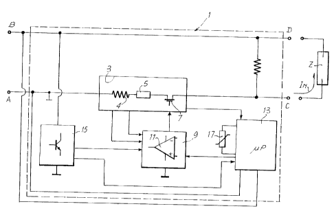
With reference initially to the diagram in Fig.1, the circuit breaker,
designated as a whole by 1, has an input consisting of two terminals, A and B,
and an output consisting'of two terminals, C and D. On the line A-C there is
set a block 3 which contains a current-read resistor 4, by means of which the
current that traverses the circuit breaker and that supplies a load circuit,
or
load, which is connected between the output terminals C and D, is read. The
block 3 moreover contains at least one fuse 5 and one electronic switch 7.
The fuse 5 constitutes a so-called "catastrophic protection"; i.e., it blows,
so
interrupting definitively the passage of current, for example in the event of
a
CA 02403603 2002-11-27
-4-
short circuit. In this case, the device must be replaced, or at least the fuse
must be replaced, whereas in other tripping situations, as will be clarified
in
what follows, it is sufficient to reset the circuit breaker that has tripped
on
account of an overcurrent. The electronic switch 7, for example a MOSFET,
constitutes a protection against transient overcurrents, and opens the circuit
in
the way described in what follows.
The reference number 9 designates a limitation block which
comprises an operational amplifier 11 and is connected both to the block 3
and to a microprocessor 13. The limitation block 9 and the microprocessor 13
are supplied by an auxiliary voltage generator 15.
In addition to being connected to the limitation block 9, the
microprocessor 13 is also connected to the block 3 and to a resistor 17 that
can vary with temperature, for example a PTC or an NTC resistor, which is
thermally coupled to the components of the circuit breaker that are subject to
overheating.
Operation of the device outlined above is as described in what
follows. In conditions of normal supply to the load Z (applied to the
terminals
C, D of the device), a current IN is supplied. The fuse 5 is intact, and the
MOSFET 7 is in full conduction.
In the case of a catastrophic event, such as a short circuit, the fuse 5
causes the circuit breaker 1 to open the circuit instantaneously and
irreversibly, and power supply to the load is thus interrupted.
In the event of overcurrent to the load Z, i.e., in the event of the
current exceeding a pre-set limit value llim;t, the limitation block 9, by
means of
the operational amplifier 11, sends the MOSFET 7 of the block 3 into a
condition of partial inhibition. The time required for this inhibition to
occur is
very short, i.e., in the region of 300 microseconds or even less. The current
that is now flowing through the circuit breaker is kept below a value lilmit
for a
delay time that can be programmed by means of the microprocessor 13. Once
this time interval has elapsed, the microprocessor 13 causes complete
inhibition of the MOSFET 7 or other equivalent switching device, so bringing
the current on the load to a stand-by value Istana_by that is very limited.
Fig. 3 shows the tripping characteristic of the circuit breaker in these
conditions. The time appears on the abscissa, and the current values appear
CA 02403603 2002-11-27
-5-
on the ordinate, as indicated above. The graph shows the plots of the nominal
or rated current Inom and the maximum current Imax for which the circuit
breaker is designed. The peak-current value is designated by lpeak, this value
being reached in a very short time interval Ts, i.e., the time needed for the
limitation block 9 to go into action. The delay time between intervention of
the
limitation block 9 and intervention of the microprocessor 13 (tripping) is
designated by Td.
The resistor 17, which is variable according to the temperature,
constitutes a temperature sensor for the microprocessor 13, said temperature
sensor enabling interruption of power supply in the event of overheating, by
means of appropriate programming of the microprocessor itself.
Since the microprocessor 13 is connected to the block 3, it can
determine, by means of the current-read resistor 4, the current
instantaneously flowing through the circuit breaker. A connection between the
terminals A and B moreover enables the instantaneous voltage to be read,
and hence enables opening of the circuit, which is controlled by the
microprocessor itself, also in the event of overvoltage.
Fig. 2 presents a more detailed diagram of an embodiment of the
circuit breaker according to the invention, in which there are shown only the
components that are essential for enabling understanding and reproduction of
the invention. The same reference numbers designate parts that are the same
as or correspond to those appearing in the block diagram of Fig. 1.
The circuit of Fig. 2 comprises three blocks, indicated by 3A, 3B, 3C,
that are functionally equivalent to block 3 of Fig. 1, the said blocks being
connected in parallel together and being basically the same as one another.
The blocks 3 may vary in number according to the maximum current for which
the circuit breaker has been sized. The larger the current for which the
circuit
breaker is to be sized, the greater the number of blocks 3, 3A, 3B, 3C, ...,
set
in parallel, each being traversed by a fraction of the total current supplied
to
the load Z.
Each block 3A, 3B, 3C comprises an operational amplifier 11, the
output of which is connected to the gate terminal of the MOSFET 7. The
source terminal of the MOSFET 7 is connected to the terminal A of the circuit
breaker 1, whilst the drain terminal is connected to the terminal C. The
CA 02403603 2002-11-27
-6-
current-read resistor is designated by 4, and the fuse is designated by 5,
both
of these being set between the source terminal of the MOSFET 7 and the
terminal A of the circuit breaker 1. Set between the output of the operational
amplifier 11 and the gate terminal of the MOSFET 7 is a further protection
fuse 21, which is set in series to a parallel-RC cell.
The inverting input of the operational amplifier 11 of each block 3A,
3B, 3C is connected, by means of a resistor 22, between the current-read
resistor 4 and the fuse 5, whilst applied to the non-inverting terminal of the
amplifier itself is a reference voltage Vref, which is generated by a circuit,
designated as a whole by 23, which is connected to the microprocessor 13
and is described in greater detail in what follows.
The voltage across the current-read resistor 4 is applied to the inputs
of an operational amplifier 25, the output of which is connected to the
microprocessor 13, which thus receives a signal that is proportional to the
current flowing through the resistor 4. The circuit arrangement described so
far is envisaged only for the block 3A, whereas it is absent in the blocks 3B
and 3C. Since the three blocks 3A, 3B, 3C are basically the same, the total
current supplied to the load Z is equal to three times the current read by the
microprocessor 13 by means of the current-read resistor 4 through the
amplifier 25.
In the circuit diagram of Fig. 2, two terminals 27 are shown, which are
connected, by means of an interface 28, to an input/output terminal 29, which
constitutes a connection of the microprocessor 13 with the outside world. By
means of this interface, the microprocessor 13 can be programmed and
interrogated, for example to check the operating conditions of the device.
Interrogation and programming can be carried out also remotely.
The reference number 31 designates a reset terminal of the
microprocessor 13, whilst 33 designates a terminal via which the
microprocessor 13 is connected to the blocks 3A, 3B, 3C. More in particular,
the terminal 33 is connected to the inverting input of each operational
amplifier 11 of the various blocks 3A, 3B, 3C through a transistor 35 and a
corresponding diode 37. Connection between each diode 37 and the
corresponding inverting input of the corresponding operational amplifier 11 is
represented by the letter X.
CA 02403603 2002-11-27
-7-
Also shown in the diagram of Fig. 2 are two LEDs, 41 and 43, which
are connected to corresponding pins of the microprocessor 13 and which
enable display of the operating conditions of the circuit breaker 1, and a
storage block 45 connected to the microprocessor 13, in which the information
regarding the operating conditions of the circuit breaker 1 is stored, this
information being readable by means of the input/output terminal 29.
The circuit 23 comprises an operational amplifier 24, the inverting
input of which is connected to the microprocessor 13, and on the output of
which there is present the reference voltage Vref. The value of the latter is
programmable by means of the microprocessor 13 according to the
characteristics that the circuit breaker 1 is to possess.
Fig. 2 is a schematic representation of the configuration, in itself
known, of the auxiliary voltage generator 15, connected to the two terminals A
and B of the circuit breaker 1. The auxiliary voltage generator 15 generates
two DC voltages, e.g., 12 V and 3 V, on the terminals designated by Vcc and
3V. These voltages are used to supply the various circuit components,
according to what is illustrated in the diagram of Fig. 2.
In line with what has been briefly described with reference to the block
diagram of Fig. 1, the circuit of Fig. 2 operates as described in what
follows. In
normal operating conditions, the current flows through the blocks 3A, 3B, 3C
towards the load Z. The MOSFETs 7 are in full conduction. In the event of
overcurrent, there is the intervention of each of the operational amplifiers
11.
The value at which the latter go into action is fixed by the reference voltage
Vref, which is determined by a corresponding programming of the
microprocessor 13. The time for intervention of the individual operational
amplifiers 11 is very limited (less than 300 microseconds), and they have the
effect of reducing the current flowing from the terminal A to the terminal C
towards the load. After a programmable delay time, the microprocessor 13
goes into action, by means of the output voltage on the pin 33 sent to the
individual amplifiers 11 of the blocks 3A, 3B, 3C, and sends the individual
MOSFETs 7 into a state of inhibition, thus reducing the current to the
tripping
value Istand_by. The microprocessor can act on the blocks 3, causing
inhibition
of the switches 7 also in the case of overheating, which is detected by the
resistor 17, which is temperature-variable.
CA 02403603 2002-11-27
-8-
It is understood that the drawings only illustrate a possible
exemplification of the invention, which may vary in its embodiments and
arrangements without thereby departing from the scope of the underlying
idea. The possible presence of reference numbers in the attached claims has
the purpose of facilitating reading thereof in the light of the foregoing
description and of the attached drawings, and in no way limits the scope of
protection represented by the claims.