Note: Descriptions are shown in the official language in which they were submitted.
CA 02463653 2004-04-13
WO 2004/006218 PCT/JP2003/008670
1
D E S C R I P T I 0 N
DRIVING DEVICE, DISPLAY APPARATUS USING
THE SAME, AND DRIVING METHOD THEREFOR
Technical Field
The present invention relates to a driving device,
a display apparatus using the driving device, and a
driving method for the display apparatus and, more
particularly, to a driving device for driving a
current-driven optical element, a display apparatus for
driving a simple matrix type display panel having,
display elements formed from a current-driven optical
elements by using the driving device, and a driving
method for the display apparatus.
Background Art
The recent years have seen a considerable
proliferation of display apparatuses and devices, such
as liquid crystal displays (LCDs), replacing
cathode-ray tubes (CRTs), as the monitors and displays
of personal computers and video equipment. Liquid
crystal displays, in particular, have quickly come into
widespread use because they can achieve decreases in
thickness and weight, space saving, a reduction in
power consumption, and the like as compared with
conventional display apparatuses (CRTs). In addition,
relatively small liquid crystal display apparatuses
have been widely used as display devices for cell
CA 02463653 2004-04-13
WO 2004/006218 PCT/JP2003/008670
2
phones, digital cameras, personal digital assistants
(Pl7As), and the like which have recently become
considerably popularized.
The following are expected as next-generation
display devices (displays) and display elements
following such liquid crystal displays: organic
electroluminescence elements (to be abbreviated as
"organic EL elements" hereinafter), inorganic
electroluminescence elements (to be abbreviated as
"inorganic EL elements" hereinafter), and display
devices having spontaneous emission type optical
elements such as light-emitting diodes (LEDs).
Among the above display devices having various
kinds of spontaneous emission type display elements,
display devices having display elements formed from
organic EL elements made of organic compounds as
light-.emitting materials have recently undergone
vigorous research and development toward practical
application and commercialization because technical
achievements superior to those obtained in other kinds
of display elements have been obtained in terms of
color display, low-voltage drive techniques, and the
like.
FIGS. 13A, 13B, and 13C respectively show the
schematic arrangement of an organic EL element, its
voltage-current characteristic, and an equivalent
circuit of the organic EL element. The structure,
CA 02463653 2004-04-13
WO 2004/006218 PCT/JP2003/008670
3
emission principle, and emission characteristics of
the organic EL element will be briefly described below.
As shown in FIG. 13A, for example, an organic EL
element OEL has an arrangement in which an anode
electrode (positive electrode) 112 made of
a transparent electrode material such as ITO (Indium
Thin Oxide), an organic EL layer 113 made of
a light-emitting material such as an organic compound,
and a cathode electrode (negative electrode) 114 made
of a metal material and having a reflection
characteristic are sequentially stacked on one surface
of a transparent insulating substrate 111 such as
a glass substrate. The organic EL layer 113 is formed
by, for example, stacking a hole transport layer 113a
made of a polymer-based hole transport material and
an electron transport light-emitting layer 113b made of
a polymer-based electron transport light-emitting _
material.
In the organic EL element OEL, as shown FIG. 13A,
when positive and negative voltages are applied from
a DC voltage source VDC to the anode electrode 112 and
cathode electrode 114, respectively, light by is
emitted on the basis of the energy produced when holes
injected into the hole transport layer 113a recombine
with electrons injected into the electron transport
light-emitting layer 113b within the organic EL
layer 113. For example, the light by is transmitted
CA 02463653 2004-04-13
WO 2004/006218 PCT/JP2003/008670
4
through the anode electrode 112 and emerges from the
other surface side (upper side in FIG. 13A) of the
insulting substrate 111. In this case, the emission
intensity (i.e., the emission luminance of the organic
EL element) of the light by is controlled in accordance
with the amount of current flowing between the anode
electrode 112 and the cathode electrode 114.
In this case, the voltage-current characteristic
of an equivalent circuit of the organic EL element OEL
exhibits a similar tendency to that of a diode, as
shown in FIG. 13B, and the electrode layers (anode
electrode 112 and cathode electrode 114) oppose each
other through the relatively thin dielectric layer
(organic EL layer 113). As shown in FIG. 13C,
therefore, the optical element can be expressed as a
parallel connection of a diode type light-emitting
element Ep and a junction Capacitance.Cp. Note that
the voltage-current characteristic of the organic EL
element will be described in detail later in the
embodiments of the present invention (to be described
later) .
As display driving methods for display apparatuses
having display panels in which display elements
(display pixels) having spontaneous emission type
optical elements such as organic EL elements like those
described above are arranged in the form of a matrix,
the active matrix driuing scheme and simple matrix
CA 02463653 2004-04-13
WO 2004/006218 PCT/JP2003/008670
(passive matrix) driving scheme are known. As is
known, in the active matrix driving scheme, a selection
switch and storage capacitance are provided for each
display pixel to control the driven state (emission
5 state) of each display element in accordance with the
charge voltage of a corresponding one of the storage
capacitances in the simple matrix driving scheme,
the emission state of each display pixel is
time-divisionally controlled by directly applying
a predetermined pulse to the display element.
Although the active matrix driving scheme is
superior to the passive one in terms of luminance and
multi-gradation for image display, a pixel driving
function such as a selection switch (thin-film
transistor) must be provided for each display pixel.
This complicates the apparatus arrangement and demands
a more advanced micropatterning technique, resulting in.
an increase in product cost. In contrast to this, in
the simple matrix driving scheme, there is no need to
prepare a pixel driving function such as a selection
switch for each display pixel, and hence the apparatus
arrangement can be simplified. This makes it possible
to improve the manufacturing yield and reduce the
product cost.
The schematic arrangement of a display apparatus
based on the simple matrix driving scheme will be
described below.
CA 02463653 2004-04-13
WO 2004/006218 PCT/JP2003/008670
6
FIG. 14 shows an example of the display apparatus
based on the simple matrix driving scheme.
As shown in FIG. 14, the display apparatus based
on the simple matrix driving scheme is roughly
comprised of a display panel 110P having a plurality of
scanning lines SL extended in a row direction, a
plurality of signal lines DL extended in a column
direction to intersect the scanning lines SL at right
angles, and display elements (organic EL elements) OEL
each formed near the intersection of the scanning line
SL and the signal line DL. The apparatus further
includes a scanning driver 120P which applies a
scanning signal to each scanning line SL at a
predetermined timing to sequentially scan the organic
EL elements OEL on each row in the selected state, a
data driver 130P which generates a driving current
corresponding to display data and supplies the current
to each organic EL element OEL through a corresponding
one of the signal lines DL in synchronism with scanning
by the scanning driver 120P, and a controller 140P
which generates a scanning control signal, data control
signal, and display data which are used to display
desired image information on the display panel 110P,
and supplies them to the scanning driver 120P and data
driver 130P.
As driving methods for the display apparatus
having the above arrangement, the following two methods
CA 02463653 2004-04-13
WO 2004/006218 PCT/JP2003/008670
7
are known. One method is a current designation type
driving method in which. the scanning driver 120P
sequentially applies a scanning signal for selecting
one of the scanning lines SL to the scanning line SL of
each row on the basis of a scanning control signal
supplied from the controller 140P in each predetermined
scanning period, and the data driver 130P generates a
driving current having a predetermined current value
corresponding to display data in the scanning period on
the basis of a data control signal and display data
supplied from the controller 140P in synchronism with
this scanning signal, and simultaneously supplies
driving currents through the respective signal
lines DL. Thus the respective organic EL elements OEL
on a selected row emit light with a predetermined
luminance level. The other method is a pulse width
modulation type driving method in which the data driver
130P generates a driving current formed from a constant
current value and having a signal time width (pulse
signal width) corresponding to display data, and
supplies the current to each signal line DL. Thus the
respective organic EL elements OEL on a selected row
emit light with a predetermined luminance level.
This operation is sequentially repeated for each row
corresponding to one frame on the display panel to
display desired image information on the display
panel 110P.
CA 02463653 2004-04-13
WO 2004/006218 PCT/JP2003/008670
8
In the simple matrix driving scheme, a voltage
driving scheme of driving each display element by
applying a predetermined voltage from the data driver
to the display element is known in addition to the
above current driving scheme. Assume that the organic
EL element is used as a display element. In this case,
since each. element has an arrangement in which the
diode type light-emitting element Ep and junction
capacitance Cp are connected in parallel as shown in
FIG. 14, and each. organic EL element OEL is connected
in parallel with the signal line DL, the total sum of
junction capacitances becomes large, and the
interconnection capacitance of each signal line is
added. As a consequence, in the voltage driving
scheme, a delay occurs in the driven state of
each display element or a voltage drop occurs in
accordance with the distance from the data driver,
resulting in, for example, variations in emission state
(luminance) in the upper and lower areas of the display
panel. This leads to a deterioration in display image
quality. In a display apparatus using organic EL
elements as display elements, therefore, the current
driving scheme is regarded superior to the voltage
driving scheme.
The display apparatus based on the above simple
matrix driving scheme, however, has the following
problems.
CA 02463653 2004-04-13
WO 2004/006218 PCT/JP2003/008670
9
In the current driving scheme, operating a display
element with a predetermined luminance level by
supplying a predetermined driving current to it is
equivalent to charging the junction capacitance or the
like of a given display element with.a driving current
and also charging the junction capacitance of the
remaining unselected display elements on a signal line
to which the given display element is connected. In
this case, as compared with the voltage driving scheme,
a deterioration in response characteristic or the
occurrence of variations in emission luminance can be
suppressed by supplying a driving current having a
large current value. Assume, however, that the driving
current supplied from the data driver is set to a
relatively small current value for the sake of the
specifications of a power supply or power saving, or
the total sum of the junction capacitances of display
elements increases as the number of scanning lines
increases and the number of display pixels increases
along with increases in the size and resolution of a
display panel. In this case, when the driving current
is supplied to the display element at a driving timing,
the response characteristics with respect to current
and voltage values deteriorate, and the time required
for a voltage applied to the display element to reach
a predetermined value is prolonged, resulting in
a noticeable lack of emission luminance and occurrence
CA 02463653 2004-04-13
WO 2004/006218 PCT/JP2003/008670
of variations.
FIG. 15A shows a change in supply current over
time when a driving current is supplied to a display
element. FIG. 15B shows a change in voltage applied to
5 a display element over time. Referring to FIG. 15A,
the abscissa represents the time; and, the ordinate,
the supply current to the display element. Reference
symbol Tspy denotes a supply period of a driving
current; and Tdly, a delay time from the start of
10 supply of the driving current to the start of operation
of the display element. Referring to FIG. 15B, the
abscissa represents the time; and the ordinate, the
voltage applied to a display pixel in the forward
direction. Reference symbol Vth denotes a threshold
voltage for operation in the display element. As shown
in FIGS. 15A and 15B, the rise characteristics of a
current value and voltage value supplied. to the display
element deteriorate owing to the junction capacitance
of the display element and the interconnection
capacitance of a signal line. In addition, owing to
variations in junction capacitance among the respective
display elements, differences in interconnection
capacitance among signal lines, and the like, the
degree of deterioration varies. As a consequence, the
amount of electric charges supplied to the display
element in a driving current supply period decreases
below the amount required for display with a desired
CA 02463653 2004-04-13
WO 2004/006218 PCT/JP2003/008670
11
luminance level, resulting in a lack of emission
luminance or variations in emission luminance among the
display elements. This leads to a deterioration in
display state.
Disclosure of Invention
According to the present invention, in a driving
device which drives a plurality of current-driven
optical elements, the response speed of each. optical
element can be increased, and hence each optical
element can be properly driven even if a driving
current to be supplied to each optical element is set
to a relatively small current value.
In addition, in a display apparatus to which the
driving device is applied and which drives a display
panel having a plurality of current-driven display
elements, the response speed of each display element in
the entire area. of the display panel is_in.creased to.
obtain good display image quality in accordance with a
display gray level, and the power consumption
associated with supply of a driving current to each
display element can be reduced.
In order to obtain the above effects, according to
the present invention, there is provided a driving
device which supplies a current to a plurality of
current-driven optical elements to drive the optical
elements, comprising at least a driving current supply
circuit which supplies a driving current to each
CA 02463653 2004-04-13
WO 2004/006218 PCT/JP2003/008670
12
optical element for a predetermined period, and
a control voltage applying circuit which applies at
least a charge voltage having a voltage value
corresponding to a voltage to be applied to each
optical element using the driving current, before the
driving current is supplied.
The driving current supplied to each optical
element has the same current value with respect to each
optical element.
The driving current supply circuit comprises a
single constant current generating circuit which
outputs a constant current having the same current
value as that of the driving current, and a plurality
of current storage circuits which sequentially receive
and hold the constant current and output the driving
current on the basis of the constant current.
Alternatively, the driving current supply circuit
further comprises a single input current storage
circuit which is provided between the constant current
generating circuit and the plurality of current storage
circuits, receives the constant current output from the
constant current generating circuit, holds a voltage
component corresponding to a current value of the
constant current, and supplies a current based on the
voltage component to the plurality of current storage
circuits.
The input current storage circuit and each of
CA 02463653 2004-04-13
WO 2004/006218 PCT/JP2003/008670
13
the current storage circuits include a capacitance
element which receives the constant current output from
the constant current generating circuit and in which
electric charge corresponding to a current value of the
constant current is written as a voltage component.
The control voltage applying circuit further
comprises means for applying a discharge voltage having
a voltage value for causing each optical element to
perform discharging operation, after the driving
current is supplied to each optical element.
The driving device also comprises a pulse width
control circuit which controls a pulse width of the
driving current applied to each optical element in
accordance with a luminance level component of a
display signal.
In order to obtain the above effects, according to
the present invention, there is provided a display
apparatus which displays image information by supplying
a driving current corresponding to a display signal to
each of a plurality of current-driven display elements
of a display panel, comprising a display panel
including a plurality of signal lines and a plurality
of scanning lines intersecting at right angles, and
the plurality of display elements arranged near
intersections of the signal lines and the scanning
lines, a scanning control circuit which sequentially
scans the scanning lines to sequentially set
CA 02463653 2004-04-13
WO 2004/006218 PCT/JP2003/008670
14
the display elements connected to the scanning lines in
a selected state, and a signal control circuit
including at least a driving current supply circuit
which supplies a driving current to each signal line
for a predetermined period, and a control voltage
applying circuit which applies, to each signal line,
a charge voltage having a voltage value based on
a voltage applied to each display element upon
application of the driving current, before supply of
the driving current. The display element comprises
an optical element, which is, for example, an organic
electroluminescence element, the organic
electroluminescence element having an anode electrode
connected to the signal line, and a cathode electrode
connected to the scanning line.
The charge voltage has at least a voltage value
which is higher than a threshold voltage_for each .
display element of the display panel and smaller than
a maximum value of a voltage value applied to each
display element when the driving current is supplied to
each display element through each signal line.
Alternatively, the charge voltage has a voltage value
equal to an average value of voltage values applied to
the respective display elements when the driving
current is supplied to the respective display elements
through. the respective signal lines.
The driving current supplied to each signal line
CA 02463653 2004-04-13
WO 2004/006218 PCT/JP2003/008670
of the display panel has the same current value for
each signal line.
The signal control circuit comprises at least a
control section which performs supply of the driving
5 current by the driving current supply circuit and
application of the charge voltage by the control
voltage applying circuit in accordance with a timing at
which the scanning control circuit sets the display
element in a selected state. '
10 The driving current supply circuit in the signal
control circuit comprises a single constant current
generating circuit which outputs a constant current
having a predetermined current value, and a plurality
of current storage circuits which are provided in
15 correspondence with the plurality of signal lines,
sequentially receive and hold the constant current, and
simultaneously output the driving currents_to the
plurality of signal lines on the basis of the constant
current. Alternatively, the driving current supply
circuit further comprises a single input current
storage circuit which is provided between the constant
current generating circuit and the plurality of current
storage circuits, receives the constant current output
from the constant current generating circuit, holds a
voltage component corresponding to a current value of
the constant current, and supplies a current based on
the voltage component to the plurality of current
CA 02463653 2004-04-13
WO 2004/006218 PCT/JP2003/008670
16
storage circuits.
The current storage circuit and input current
storage circuit each include a capacitance element
which receives the constant current output from the
constant current generating circuit and in which
electric charge corresponding to the constant current
is written as the voltage component.
The control voltage applying circuit in the signal
control circuit further comprises means for applying,
to each signal line, a discharge voltage which causes
each display element to perform discharging operation
and does not exceed a threshold voltage of the display
element, after the driving current is supplied to each
signal line.
The signal control circuit comprises a pulse width
control circuit which controls a pulse width of the
driving current to each signal line in accordance_with
a luminance level component of a display signal.
Brief Description of Drawings
The accompanying drawings, which are incorporated
in and constitute a part of the specification,
illustrate embodiments of the invention, and together
with the general description given above and the
detailed description of the embodiments given below,
serve to explain the principles of the invention.
FIG. 1 is a block diagram showing an example of
the overall arrangement of a driving device and
CA 02463653 2004-04-13
WO 2004/006218 PCT/JP2003/008670
17
a display apparatus using the driving device;
FIG. 2 is a schematic circuit diagram showing the
arrangement of a part of the display apparatus to which
the present invention can be applied;
FIG. 3 is a circuit diagram showing the
arrangement of a part of a data driver which can be
applied to the driving device according to the present
invention;
FIG. 4 is a timing chart showing control operation
in a scanning driver and the data driver which can be
applied to the present invention;
FIG. 5 is a graph showing voltage-current
characteristics representing the relationship between
voltages applied by the scanning driver and data driver
which can be applied to the present invention;
FIG. 6 is a timing chart showing display driving
operation in the display apparatus to which the present
invention can be applied;
FIG. 7 is a schematic block diagram showing a
first embodiment of a constant current supply circuit
which can be applied to the driving apparatus according
to the present invention;
FIG. 8 is a circuit diagram showing a specific
example of a current generating circuit which can be
applied to the constant current supply circuit
according t~ the present invention;
FIG. 9 is a circuit diagram showing a specific
CA 02463653 2004-04-13
WO 2004/006218 PCT/JP2003/008670
18
example of an arrangement constituted by a current
storage circuit and switch means which can be applied
to the constant current supply circuit according to the
present invention;
FIGS. 10A and 10B are circuit diagrams showing
basic operation in a current storage circuit which can
be applied to the constant current supply circuit
according to the present invention;
FIG. 11 is a schematic block diagram showing a
second embodiment of the constant current supply
circuit which can be applied to the driving device
according to the present invention;
FIG. 12 is a schematic block diagram showing a
third embodiment of the constant current supply circuit
which can be applied to the driving device according to
the present invention;
FIG. 13A is a sectional view showing the schematic
arrangement of an organic EL element;
FIG. 13B is a graph showing the approximate
voltage-current characteristic of the organic EL
element;
FIG. 13C is an equivalent circuit diagram of the
organic EL element;
FIG. 14 is a view showing an example of a display
apparatus based on the simple matrix driving scheme;
FIG. 15A is a graph showing a change in supply
current over time when a driving current is supplied to
CA 02463653 2004-04-13
WO 2004/006218 PCT/JP2003/008670
19
an organic EL element; and
FIG. 15B is a graph showing a change in voltage
applied to a display element over time when a driving
current is supplied to an organic EL element.
Best Mode for Carrying Out the Invention
Embodiments of a driving device, a display
apparatus using the driving device, and a driving
method for the display apparatus according to the
present invention will be described in detail below.
<Arrangement of Display Apparatus>
The schematic arrangement of a driving device
according to the present invention and a display
apparatus to which the driving device can be applied
will be described first with reference to the several
views of the accompanying drawing.
FIG. 1 is a block diagram showing an example of
the overall.arrangement of the driving device_according
to the present invention and the display apparatus to
which the driving device can be applied. FIG. 2 is a
schematic circuit diagram showing the arrangement of
the main part of the display apparatus to which the
present invention can be applied.
In the following description, organic EL elements
OEL are used as display elements for a display panel.
However, the display apparatus according to the present
invention is not limited to this. The present
invention can also be suitably applied to a case
CA 02463653 2004-04-13
WO 2004/006218 PCT/JP2003/008670
wherein optical elements such as light-emitting diodes
(LEDs) are used as display elements instead of organic
EL elements.
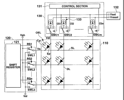
As shown in FIGS. 1 and 2, a display apparatus 100
5 to which the present invention can be applied is
comprised of a display panel (pixel array) 110,
scanning driver (scanning control circuit) 120, data
driver (signal control circuit) 130, system controller
140, and display signal generating circuit 150. In the
10 display panel 110, display elements including, for
example, organic EL elements OEL are formed near the
intersections of a plurality of scanning lines SL and a
plurality of signal lines DL which are arranged in
orthogonal directions. The scanning driver 120 is
15 connected to the scanning lines SL of the display panel
110 and controls the display elements on each row in
the selected state by sequentially applying.a scanning
signal Vs to each scanning line SL at a predetermined
timing. The data driver 130 is connected to the signal
20 lines DL of the display panel 110, supplies a constant
current (driving current) Ic having a signal time width
(pulse width) corresponding to display data in
synchronism with the application timing of the scanning
signal Vs, and applies a set voltage Vset (charge
voltage) or reset voltage Vreset (discharge voltage) at
a predetermined timing. The system controller 140
generates and outputs at least a scanning control
CA 02463653 2004-04-13
WO 2004/006218 PCT/JP2003/008670
21
signal and data control signal for controlling the
operation states of the scanning driver 120 and data
driver 130, on the basis of a timing signal supplied
from the display signal generating circuit 150. The
display signal generating circuit 150 supplies the
above display data to the data driver 130 on the basis
of a video signal supplied from the outside of the
display apparatus 100, generates a timing signal
(system clock or the like) for operating each organic
EL element in a predetermined driven state on the basis
of the display data, and supplies the timing signal to
the system controller 140.
The arrangement of each of the above components
will be described below.
(Display Panel)
As shown in FIG. 2, the display panel 110 which
can be applied to the present invention has n scanning
line SL and m signal lines DL which are intersecting
each other at right angles. The display panel 110 has
a simple matrix arrangement in which the organic EL
elements OEL each having the cross-sectional structure
shown in FIG. 13A are formed at the intersections of
the respective signal lines DL and the respective
scanning lines SL with the anode electrodes (positive
electrodes) and cathode electrodes (negative
electrodes) of the elements being connected to
the signal lines DL and the scanning lines SL,
CA 02463653 2004-04-13
WO 2004/006218 PCT/JP2003/008670
22
respectively. In this case, each organic EL element
OEL has an arrangement in which a diode type display
element Ep and a junction capacitance Ca are connected
in parallel as in FIG. 14.
(Scanning Driver}
The scanning driver 120 sets display elements on
each row in the selected state by sequentially applying
the scanning signal Vs (= Vsl) to each scanning line SL
on the basis of a scanning control signal supplied from
the system controller 140, thereby performing control
to write the constant driving current Ic supplied from
the data driver 130 through the signal line DL and
apply the predetermined reset voltage Vreset.
As shown in FIG. 2, the scanning driver 120 is
comprised of a shift register 121, switches SWL1,
SWL2,..., SWLn (to be also referred to as "switches
SWL" herein after for the sake of convenience), _
high-voltage power supply, and low-voltage power
supply. The shift register 121 sequentially outputs
shift output signals RS1, RS2,..., RSn (to be also
referred to as "shift output signals RS" hereinafter
for the sake of convenience) on the basis of scanning
control signals (a shift start signal, shift clock, and
the like) supplied from the system controller 140. The
switches SWL1, SWL2,..., SWLn are provided for the
respective scanning lines SL, and the contacts of the
switches are switched on the basis of the shift output
CA 02463653 2004-04-13
WO 2004/006218 PCT/JP2003/008670
23
signals RS1, RS2,..., RSn. The high-voltage power
supply commonly applies a signal voltage Vsh (charge
control voltage) of a predetermined high voltage (high
level) to one of the switching contacts of each of the
switches SWL1, SWL2,..., SWLn. The low-voltage power
supply commonly applies a signal voltage Vsl (driving
control voltage) of a predetermined low voltage (low
level) to the other of the switching contacts of each
of the switches SWL1, SWL2,..., SWLn. When the shift
output signals RS1, RS2,..., RSn which are generated by
the shift register 121 while it sequentially shifts
from the upper side of the display panel 110 to the
lower side are input to the switches SWL1, SWL2,...,
SWLn, the switching contacts are sequentially switched
to the low-voltage power supply side. As a
consequence, the scanning signal Vs having the
low-level signal voltage Vsl is applied to_the anode
electrodes of the organic EL elements OEL on the
selected row (scanning line) for only a predetermined
period (the supply period of the driving current Ic and
the application period of the reset voltage Vreset in
one scanning period). Note that in a state wherein the
shift output signals RS1, RS2,... are not input from
the shift register 121 to the switches SWL1, SWL2,...,
SWLn (no row is selected), the switching contacts of
the switches SWL1, SWL2,..., SWLn are switched to the
power supply side, and the scanning signal Vs having
CA 02463653 2004-04-13
WO 2004/006218 PCT/JP2003/008670
24
the high-level signal voltage Vsh is applied. Each
switch SWL is formed from a switch element such as
a field-effect transistor.
(Data Driver)
FIG. 3 is a circuit diagram showing the
arrangement of the main part of the data driver which
can be applied to the driving device according to
the present invention.
The data driver 130 sequentially receives and
holds display data line by line supplied from the
display signal generating circuit 150 at a
predetermined timing on the basis of various data
control signals (an output enable signal, output
control signal, shift start signal, shift clock, and
the like) supplied from the system controller 140.
The data driver 130 converts each display data into
a current component of a constant value with a signal
time width (pulse width) corresponding to the luminance
level of the display data, and supplies the data to
each signal line DL at a predetermined timing within
a scanning period set for each of the above scanning
lines.
As shown in FIG. 2, the data driver 130 is
comprised of a control section 131, switches SWC1,
SWC2,..., SWCm (to be also referred to as "switches
SWC" hereinafter for the sake of convenience),
a control voltage applying circuit 132, and constant
CA 02463653 2004-04-13
WO 2004/006218 PCT/JP2003/008670
current supply circuits 133 (driving current supply
circuits). The control section 131 outputs control
signal CS1, CS2,..., CSm in accordance with a timing at
which the scanning driver 120 sets display elements on
5 each row in the selected state by applying the scanning
signal Vs to each scanning line SL on the basis of data
control signals (output control signals and the like)
supplied from the system controller 140. The switches
SWC1, SWC2,..., SWCm are provided for the respective
10 signal lines DL, and the contacts of the switches are
switched on the basis of control signal CS1, CS2,...,
CSm supplied from the control section 131. The control
voltage applying circuit 132 commonly applies the set
voltage Vset (charge voltage) of a predetermined high
15 voltage (high level) to the first switching contacts of
the switches SWC1, SWC2,..., SWCm, and commonly applies
the reset voltage Vreset (discharge voltage) of a
predetermined low voltage (low level) to the third
switching contacts of the switches SWC1, SWC2,...,
20 SWCm. The set voltage Vset is set to a value
corresponding to a potential to be applied to
the display element by supplying the constant driving
current Ic and that is equal to or more than at least
the threshold voltage of the display element and does
25 not exceed the maximum voltage applied to each display
element when the driving current Ic is supplied. More
preferably, the set voltage Vset is set to the average
CA 02463653 2004-04-13
WO 2004/006218 PCT/JP2003/008670
26
voltage of the maximum voltage and minimum voltage at
the signal line DL when the driving current Ic is
supplied. The reset voltage Vreset is set to a value
that can temporarily release and reset the charge of
the signal line DL and ,for example, set to ground
potential (0 V). More preferably the reset voltage
Vreset is set to be slightly lower than the threshold
voltage of the display element. Each of the constant
current supply circuits 133 supplies the driving
current Ic having a constant current value and a signal
time width (pulse width) based on the luminance
graduation component of display data to the second
switching contact of a corresponding one of the
switches SWC1, SWC2,..., SWCm. A constant current
supply circuit which can be applied to the data driver
according to the present invention will be described in
detailed later.
FIG. 3 is a circuit diagram showing an example of
an arrangement of the switches SWC which can be applied
to the data driver 130. For example, as shown in
FIG. 3, each of the switches SWC1, SWC2,..., SWCm
provided for the respective signal lines DL of the data
driver 130 can have an arrangement including a switch
element (to be referred to as an "NMOS transistor"
hereinafter) Trll, NMOS transistor Trl2, and switch
element (to be referred to as a "PMOS transistor"
hereinafter) Trl3. The NMOS transistor Trl1 is formed
CA 02463653 2004-04-13
WO 2004/006218 PCT/JP2003/008670
27
from an n-channel field-effect transistor and has a
source terminal connected to the high-voltage power
applying circuit 132 for applying the constant set
voltage Vset, a drain terminal connected to the signal
line DL, and a gate terminal to which a control signal
Vgs is applied at the first timing. The NMOS
transistor Trl2 has a source terminal connected to the
constant current supply circuit 133 for supplying the
constant driving current Ic, a drain terminal connected
to the signal line DL, and a gate terminal to which
a control signal Vgc is applied at the second timing.
The PMOS transistor Trl3 is formed from a p-channel
field-effect transistor and has a source terminal
connected to the low-voltage power applying circuit
134 for applying the constant reset voltage Vreset,
a drain terminal connected to the signal line DL, and
a gate terminal to which a control signal Vgr is.
applied at the third timing.
That is, the switches SWC1, SWC2,..., SWCm each
have an arrangement in which the NMOS transistors Trl1
and Trl2 and PMOS transistor Trl3 are connected in -
parallelwith the single signal line DL. The switches
SWC1, SWC2,..., SWCm are selectively turned on at
different timings to supply predetermined voltages or
currents to the signal lines DL.
The control signals Vgs, Vgc, and Vgr applied to
the gate terminals of the NMOS transistors Trl1 and
CA 02463653 2004-04-13
WO 2004/006218 PCT/JP2003/008670
28
Trl2 and the PMOS transistor Trl3 are generated on
the basis of data control signals supplied from the
system controller 140 and display data supplied from
the display signal generating circuit 150, and are
selectively applied to the respective transistors at
predetermined timings within a scanning period set for
each row (scanning line). The operations of these
switches SWC1, SWC2,..., SWCm and voltage and current
components supplied to the signal lines DL will be
described in detail later.
Referring to FIG. 3, resistance components Rpa,
Rp, and Rpb formed in series with the signal line DL
are equivalent representations of the interconnection
resistances of the signal line DL, and capacitance
components Cpa and Cpb formed on the two ends of the
signal line DL are interconnection capacitances
(parasitic capacitances).which are parasitic on th.e.
signal line DL.
(System Controller)
The system controller 140 generates and outputs,
to the scanning driver 120 and data driver 130,
a scanning control signal and data control signal
for controlling their operation states to make the
respective drivers operate at predetermined timings so
as to generate and output the scanning signal Vs,
driving current Ic, set voltage Vset, and reset voltage
Vreset. The system controller 140 then supplies
CA 02463653 2004-04-13
WO 2004/006218 PCT/JP2003/008670
29
the scanning signal Vs to the cathode electrode of each
organic EL element, and the driving current Ic, set
voltage Vset, and reset voltage Vreset to the anode
electrode of each organic EL element to make each
organic EL element operate with a predetermined
luminance level so as to display image information
based on a predetermined video signal on the display
panel 11Q.
(Display Signal Generating Circuit)
The display signal generating circuit 150 extracts
luminance level signal components from a video signal
supplied from, for example, the outside of the display
apparatus, and supplies the signal components as
display data to the data driver 130 for each line of
the display panel 110. If the above video signal
contains a timing signal component for defining the
display timing of image information like a TV broadcast
signal (composite video signal), the display signal
generating circuit 150 (FIG. 1) may have the function
of extracting a timing signal component and supplying
it to the system controller 140 as well as the function
of extracting the above luminance level signal
component. In this case, the system controller 140
described above generates a scanning control signal and
data control signal to be respectively supplied to the
scanning driver 120 and data driver 130, on the basis
of timing signals supplied from the display signal
CA 02463653 2004-04-13
WO 2004/006218 PCT/JP2003/008670
generating circuit 150.
<Driving Method for Driving Device>
The operations of the above scanning driver and
data driver and voltage and current components supplied
5 to the scanning lines and signal lines will be
described in detail next with reference to the several
views of the accompanying drawing.
FIG. 4 is a timing chart showing the control
operations (driving method) of the scanning driver and
10 data driver which can be applied to the present
invention. FIG. 5 is a graph showing voltage-current
characteristics representing the relationship between
the voltages applied from the scanning driver and data
driver which can be applied to the present invention.
15 FIG. 6 is a timing chart showing the display driving
operation of the display apparatus to which the present
invention can be applied. __ . .
In the control operations of the scanning driver
and data driver according to the present invention, as
20 shown in FIG. 4, a set period Tset during which the
above set voltage Vset (charge voltage) is applied to
each signal line DL, a constant current supply period
TC during which the driving current IC is supplied to
each signal line DL, and a reset period Treset during
25 which the reset voltage Vreset (discharge voltage) is
applied to each signal line DL are sequentially set
within a scanning period Tsel (selection period) which
CA 02463653 2004-04-13
WO 2004/006218 PCT/JP2003/008670
31
is set for each scanning line at different timings.
Note that FIG. 4 shows a case wherein the display
elements on a specific row (scanning line) are driven.
(Set Period)
In the set period Tset, as shown in FIG. 4, at the
start timing of a scanning period set for a specific
row, the high-level set control signal Vgs is applied
to the gate terminal of the NMOS transistor Trl1
provided in the data driver 130 to turn on the
transistor, and the reset high-level control signal Vgr
is applied to the gate terminal of the PMOS transistor
Trl3 to turn off the transistor. At this time, the
low-level current supply control signal VgC is applied
to the gate terminal of the NMOS transistor Trl2 to
keep it off. As a consequence, the set voltage Vset
having a predetermined high voltage (e.g., 12 V) is
applied to the signal line DL through the NMOS _
transistor Trll, and applied to the anode electrode of
the organic EL element through the signal line DL
(signal line voltage Vdl = Vset).
The set voltage Vset is set to a value
corresponding to a potential (VC) to be applied to
the display element by supplying the constant driving
current Ic to the signal line DL during the constant
current supply period TC (to be described later). That
is, as shown in FIG. 5, when the driving Current IC is
applied to the signal line DL, a voltage drop Vdrop
CA 02463653 2004-04-13
WO 2004/006218 PCT/JP2003/008670
32
occurs in accordance with the interconnection length
from the data driver 130 serving as a power supply to
the organic EL element OEL. As a consequence, a
maximum voltage Vmax is applied to the side nearest to
the data driver 130 and a minimum voltage Vmin is
applied to the side farthest from the data driver 130.
As will be described later, in order to set the organic
EL elements OEL connected to all the scanning lines SL
in the non-emission state, it suffices if the set
voltage Vset is set to a value that is equal to or more
than at least the threshold voltage (turn-on voltage)
of the organic EL element OEL and does not exceed the
maximum voltage Vmax applied to each display element
when the driving current Ic is supplied. More
preferably, in order to improve the uniformity of the
effect obtained in the overall display panel by
applying the set voltage Vset, the set voltage Vset is.
set to a voltage that can supply the driving current IC
having a constant current value to the organic EL
element OEL in the central area of the display panel
110, i.e., the average voltage of the maximum voltage
Vmax and minimum voltage Vmin at the signal line DL.
In addition, in the set period Tset, the switch
SWL provided in the scanning driver 120 is connected to
the switching contact on the high-voltage power supply
side to apply the high-level scanning signal Vs (= Vsh)
to the scanning line SL (the cathode electrode of
CA 02463653 2004-04-13
WO 2004/006218 PCT/JP2003/008670
33
the organic EL element). In this case, the high-level
scanning line Vs (= Vsh) is applied from the scanning
driver 120 to the scanning lines SL of the remaining
rows in the unselected state as well as the above
specific row.
In the set period Tset, the high-level scanning
signal Vs (= Vsh) applied to the scanning lines SL of
all the rows is set to a voltage (e. g., 9 V) at which
the organic EL elements OEL connected to all the
scanning lines SL emit no light even if the above
maximum voltage (Vmax) is applied as the set voltage
Vset to the signal line DL. More specifically, as
shown in FIG. 5 and inequality (1) given below, the
scanning signal Vs is set to be higher in voltage than
the voltage (Vmax - Vturn-on) obtained by subtracting a
turn-on voltage Vturn-on for the organic EL element OEL
from the maximum voltage value (- Vmax) applied to the
signal line DL.
Vs(= Vsh) > Vmax - Vtrun-on ~"(1)
In this case, the set voltage Vset and the
scanning signal Vs (= Vsh) having the relationship
represented by inequality (1) are respectively applied
to the anode electrode and cathode electrode of each
organic EL element QEL connected to the scanning line
of each row to produce a potential difference between
the anode electrode and the cathode electrode. In the
present invention, this potential difference causes no
CA 02463653 2004-04-13
WO 2004/006218 PCT/JP2003/008670
34
current to flow in any of the organic EL elements.
Owing to the application of each voltage in the
set period Tset, therefore, before the driving current
Ic (to be described later) is supplied (constant
current supply period Tc), the interconnection
capacitance added to the signal line DL and the
junction capacitance of each organic EL element are
quickly charged to a predetermined voltage (= Vset),
and each organic EL element is held in the non-emission
state.
(Constant Current Supply Period)
In the constant current supply period Tc, as shown
in FIG. 4, after the low-level set control signal Vgs
is applied to the gate terminal of the NMOS transistor
Trl1 provided in the data driver 130 to turn off the
transistor, the high-level current supply control
signal Vgc is applied to the gate terminal of the NMOS
transistor Trl2 to turn it on. At this time, the
high-level reset control signal Vgr is applied to the
gate terminal of the PMOS transistor Trl3 to keep it
off. As a consequence, the driving current Ic having a
constant current value is generated by the constant
current supply circuit 133 and supplied to the signal
line DL (the anode electrode of the organic EL element)
through the NMOS transistor Trl2 (organic EL element
supply current Iel = Ic).
In this case, the driving current Ic supplied from
CA 02463653 2004-04-13
WO 2004/006218 PCT/JP2003/008670
the data driver 130 to the organic EL element OEL
through the signal line DL is set to be supplied with
a predetermined signal time width (pulse width)
corresponding to the luminance level based on display
5 data supplied from the display signal generating
circuit. The voltage Vc (e.g., 12 V) applied to the
signal line DL by supplying the driving current Ic in
the constant current supply period Tc is set to be
equal to the set voltage Vset applied to the signal
10 line DL in the set period Tset (signal line voltage
Vdl = VC = Vset).
In the constant current supply period TC, the
switch SWL provided in the scanning driver 120 is
connected to the switching contact on the low-voltage
15 power supply side, and the low-level scanning signal Vs
Vsl) is applied to the scanning line SL (the cathode
electrode of the organic EL element). In. this case,
the high-level scanning signal Vs (= Vsh) is kept
applied to the scanning lines SL of the remaining rows
20 in the unselected state. The low-level scanning signal
Vs (= Vsl) is set to, for example, ground potential
( 0 V) .
Owing to the application of the respective
currents and voltages in the constant current supply
25 period Tc, the predetermined driving current IC
required to perform light emission is supplied to each
organic EL element connected to the selected scanning
CA 02463653 2004-04-13
WO 2004/006218 PCT/JP2003/008670
36
line at a predetermined signal time width (for a short
period of time when the gray level is low, and vice
versa) corresponding to display data on the basis of
a known pulse width modulation (PWM driving) control
method. As a consequence, each organic EL element
emits light with a predetermined luminance level.
In this case, since the interconnection capacitance
added to the signal line DL and the junction
capacitance of each organic EL element have been
charged to the set voltage Vset (= Vc) in the set
period Tset by the constant voltage source (the power
supply for applying the set voltage Vset), the driving
current Ic increases to the current value required for
light emission in a very short period of time after the
driving current Ic is supplied, and each organic EL
element quickly emits light.
(Reset Period) --
In the reset period Treset, as shown in FIG. 4,
after the low-level current supply control signal Vgc
is applied to the gate terminal of the NMOS transistor
Trl2 provided in the data driver 130 to turn off the
transistor, the low-level reset control signal Vgr is
applied to the gate terminal of the PMOS transistor
Trl3 to turn it on. At this time, the low-level set
control signal Vgs is applied to the gate terminal of
the NMOS transistor Trl1 to keep it off. As a
consequence, the reset voltage Vreset having
CA 02463653 2004-04-13
WO 2004/006218 PCT/JP2003/008670
37
a predetermined low voltage (e.g., 6 V) is applied to
the signal line DL (the anode electrode of the organic
EL element) through the PMOS transistor Trl3, and
the electric charge stored in the interconnection
capacitance added to the signal line DL and the element
capacitance of the organic EL element is discharged
(signal line voltage Vdl = Vreset).
The reset voltage Vreset is set to an arbitrary
potential that can temporarily release and reset the
potential of the high voltage (Vset = VC) applied to
the signal line DL during the set period Tset and
constant current supply period TC described above
and ,for example, the reset voltage Vreset is set to
ground potential (0 V). More preferably, as shown in
FIG. 5, the reset voltage Vreset is set to be slightly
lower than the turn-on voltage Vturn-on for the organic
EL element (Vreset < Vturn-on). With this setting,
when a row is repeatedly scanned and selected next, the
time required for charging operation in the set period
Tset is shortened, and the power consumption for
Charging/discharging operation is reduced as compared
with a case wherein the reset voltage Vreset is set t~
ground potential (0 V).
In this manner, the above series of operation
periods are set within a scanning period for each
scanning line constituting the display panel, as shown
in FIG. 6, thereby performing grayscale display of
CA 02463653 2004-04-13
WO 2004/006218 PCT/JP2003/008670
38
predetermined image information based on display data
on the display panel.
As described above, in the display apparatus
according to this embodiment, the set voltage Vset is
applied from the constant voltage source to the signal
line DL in a scanning period before the supply of the
driving current Ic to charge the interconnection
capacitance added to the signal line DL and the
junction capacitance of the organic EL element in
advance. This makes it possible to quickly perform
Charging/discharging operation in a short period of
time as compared with a case wherein the Capacitances
are charged by using only a constant current source.
In this case, the apparatus is resistant to the
influence of a voltage drop due to the interconnection
length of the signal line DL and the like, and can be
charged to. the substantially uniform set voltage Vset
regardless of the layout positions of the scanning
lines SL in the display panel 110.
In this case, the set voltage Vset is approximated
at the voltage Vc that is set to supply a driving
current to the organic EL element. Even if, therefore,
the set period Tset switches to the constant current
supply period Tc to supply the constant driving current
IC, the amount of adjustment of the signal line voltage
Vdl can be decreased. This makes it possible to
shorten the time required for this adjustment and
CA 02463653 2004-04-13
WO 2004/006218 PCT/JP2003/008670
39
improve the response display characteristics.
In addition, owing to quick charging operation in
the set period Tset, a relatively long operation time
(constant current supply period TC) can be ensured
within a scanning period. Even if, therefore, the
operation time (signal time width) of each organic EL
element is controlled by the pulse width modulation
control scheme, good grayscale display can be realized.
In the set period Tset, the potentials of all the
scanning lines SL are set to the voltage Vsh having a
predetermined high level. Even if, therefore, the set
voltage Vset is applied to the signal line 17L, no
current flows in any organic EL element. This shortens
the time required for precharging (charging) operation
to the set voltage Vset, thereby improving the response
characteristics.
Furthermore, in the constant current supply period
Tc, supplying the driving current Ic having a constant
current value from the constant current source can
compensate for a voltage drop at the signal line DL so
as to ensure the predetermined voltage VC. This makes
it possible to properly cope with a change in voltage
applied to the organic EL element OEL over time and
supply the constant current (driving current) IC based
on the substantially uniform voltage VC to the organic
EL element OEL, thereby realizing high display image
quality without variations in luminance level.
CA 02463653 2004-04-13
WO 2004/006218 PCT/JP2003/008670
In this case, since the pulse width modulation
control scheme of supplying the driving current Ic
having a constant current value with a time signal
width (pulse width) corresponding to the luminance
5 level component contained in display data is used for
each organic EL element OEL, it suffices if the driving
current Ic to be supplied to each. organic EL element
during the constant current supply period Tc has a
constant current value. In addition, since there is no
10 need to change/control the voltage value of the set
voltage Vset, simple circuit arrangements can be used
as a constant current source and constant voltage
source which are used to supply the above current and
voltage.
15 In the reset period Treset after the constant
current supply period Tc, the voltage value of the
reset voltage Vreset applied to the signal line DL need
not be set to ground potential (0 V) but may be set to
an arbitrary voltage equal to or less than the turn-on
20 voltage Vturn-on for the organic EL element OEL..
Therefore, the amount of electric charge to be
charged/discharged with respect to the interconnection
capacitance or the junction capacitance of the organic
EL element OEL can be reduced by the potential
25 difference (Vreset < Vturn-on). This makes it possible
to reduce power consumption.
In the reset period Treset, the reset voltage
CA 02463653 2004-04-13
WO 2004/006218 PCT/JP2003/008670
41
Vreset is applied to the signal line DL instead of
resetting all the scanning lines SL including
unselected scanning lines every time the constant
current supply period Tc (reset period) terminates.
This eliminates the necessity to perform
charging/discharging operation for the junction
capacitance of the organic EL element OEL, thus
reducing power consumption.
<First Embodiment of Constant Current Supply Circuit>
The first embodiment of a constant current supply
circuit for outputting a driving current having a
constant current value in the data driver according to
the above embodiment will be described in detail with
reference to the several views of the accompanying
drawing.
FIG. 7 is a schematic block diagram showing a
first embodiment of the constant current supply circuit
which can be applied to the data driver according to
the above embodiment.
As shown in FIG. 7, the constant current supply
circuit 133 is comprised of a single constant current
generating circuit 10A, a shift register 20A,
a plurality of switch means 40A, a plurality of current
storage circuits 30A, and a PWM control circuit 80.
The constant current generating circuit 10A generates
the driving current Ic for operating a plurality of
loads (organic EL elements OEL). The shift register
CA 02463653 2004-04-13
WO 2004/006218 PCT/JP2003/008670
42
20A sets timings at which the constant currents Ip
supplied from the constant current generating circuit
10A are sequentially supplied to the current storage
circuits 30A. The plurality of switch means 40A
control the supply states of the constant currents Ip
to the respective current storage circuits 30A in
accordance with a switching signal (shift output) SR
output from the shift register 20A at a predetermined
timing. The plurality of current storage circuits 30A
sequentially receive and hold (store) the constant
currents Ip supplied from the constant current
generating circuit 10A through the switch means 40A at
predetermined timings based on the shift register 20A.
The PWM control circuit 80 is connected to output
terminals Tout, receives display data, and sets
a signal time width (pulse width) with which
the driving current Ic is to be supplied by PWM control
based on the luminance level component contained in
the display data.
In addition, "SWC" in FIG. 7 corresponds to the
switch SWC in FIG. 2, and is a three-contact switch
provided among an output terminal of the PWM control
circuit 80, the set voltage Vset, the reset voltage
Vreset, and the signal line DZ connected to
2~5 the plurality of organic EZ elements OEZ.
The arrangement of each of the above components
will be described in detail below.
CA 02463653 2004-04-13
WO 2004/006218 PCT/JP2003/008670
43
(Current Generating Circuit)
FIG. 8 is a circuit diagram showing the
arrangement of a specific example of the current
generating circuit which can be applied to the above
constant current supply circuit or circuit 10A.
In brief, the constant current generating circuit
10A is designed to generate the constant current Ip
having a current value required to make each of the
organic EL elements operate in a predetermined emission
state and output the current to each current storage
circuit 30A provided in correspondence with
a corresponding one of the organic EL elements.
In this case, the constant current generating
circuit 10A can have a circuit arrangement including
a control current generating circuit 11 on the front
stage and an output current generating circuit 12 on
the rear stage, as shown in, for example, FIG. 8. Note
that the current generating circuit described in this
embodiment is merely an example that can be applied to
the driving device according to the present invention,
and is not limited to this circuit arrangement. This
embodiment exemplifies, as the constant current
generating circuit 10A, the arrangement having the
control current generating circuit 11 and output
current generating circuit 12. However, the present
invention is not limited to this. For example,
a circuit having a circuit arrangement formed from only
CA 02463653 2004-04-13
WO 2004/006218 PCT/JP2003/008670
44
the control current generating circuit 11 may also be
used.
For example, as shown in FIG. 8, the control
current generating circuit 11 has a circuit arrangement
including a pnp bipolar transistor (to be abbreviated
as a "pnp transistor" hereinafter) Q11 and NMOS
transistor M11. The pnp transistor has an emitter
connected to the other terminal of a resistor R11 whose
one terminal is connected to a high-potential power
supply Vdd, and a collector connected to the rear-stage
current mirror circuit section 12 (output node N11).
The NMOS transistor M11 has a source connected to the
base of the pnp transistor Q11, a drain connected to
the set terminal Tset to which a set signal SET is
input, and a gate connected to an input terminal Tin to
which a predetermined control signal IN is input.
For example, as shown in FIG. 8, the output
current generating circuit 12 has a circuit arrangement
including an npn bipolar transistor (to be abbreviated
as an "npn transistor" hereinafter) Q12, resistor R12,
npn transistor Q13, and resistor R13. The npn
transistor Q12 is formed from a current mirror circuit
and has a collector and base which are connected to the
output node N11 of the control current generating
circuit 11. The resistor R12 is connected between the
emitter of the npn transistor Q12 and a low-potential
power supply Vss. The npn transistor Q13 has
CA 02463653 2004-04-13
WO 2004/006218 PCT/JP2003/008670
a collector connected to an output terminal Tcs which
outputs an output current (constant current Ip) having
a predetermined current component, and a base connected
to the output node N11 of the control current
5 generating circuit 11. The resistor R13 is connected
between the emitter of the npn transistor Q13 and the
low-potential power supply Vss.
In this case, an output current (constant
current Ip) has a current value corresponding to
10 a predetermined current ratio which is defined by the
current mirror circuit arrangement with respect to the
current value of a control current generated by the
control current generating circuit 11 and input through
the output node N11. In this embodiment, when an
15 output current of negative polarity is supplied to the
current storage circuit 30A, a current component flows
from the current storage circuit 30A to the constant
current generating circuit 10A.
(Shift Register/Switch Means)
20 The shift register 20A sequentially applies
sequentially output shift outputs as switching signals
SR to the respective switch means 40A provided in
correspondence with the respective signal lines DZ on
the basis of control signals supplied from, for
25 example, a control section such as the system
controller 140 shown in FIG. 1. The switch means 40A
are turned on at different timings on the basis of the
CA 02463653 2004-04-13
WO 2004/006218 PCT/JP2003/008670
46
switching signals SR output from the shift register 20A
to supply the constant currents Ip from the constant
current generating circuit 10A to the current storage
circuits 30A so as to control them to receive and hold
the currents.
(Current Storage Circuit)
FIG. 9 is a circuit diagram showing an example of
an arrangement including a current storage circuit and
a switch means which can be applied to the above
constant current supply circuit. FIGS. 10A and 10B are
conceptual views showing the basic operation of a
current storage circuit which can be applied to the
above constant current supply circuit.
The current storage circuits 30A are designed to
sequentially receive and hold the constant currents Ip
output from the constant current generating circuit 10A
on the basis. of shift outputs output from the shift
register 20A and simultaneously output the held current
components directly or predetermined currents generated
on the basis of the current components, as the driving
currents Ic, to the respective signal lines DL through
the output terminals Tout.
In this case, the current storage circuit 30A can
have a circuit arrangement including a voltage
component holding section 31 (including the switch
means 40A) on the front stage and a driving current
generating section 32 on the rear stage, as shown in,
CA 02463653 2004-04-13
WO 2004/006218 PCT/JP2003/008670
47
for example, FIG. 9. Note that the current storage
circuit described in this embodiment is merely an
example that can be applied to the driving device
according to the present invention, and is not limited
to this circuit arrangement. This embodiment
exemplifies, as the current storage circuit 30A, the
arrangement having the voltage component holding
section 31 and driving current generating section 32.
However, the present invention is not limited to this.
For example, a circuit having a circuit arrangement
formed from only the voltage component holding section
31 may also be used.
For example, as shown in FIG. 9, the voltage
component holding section 31 has an arrangement
including PMOS transistors M31, M32, and M33, storage
capacitance C31, and PMOS transistor M34. The PMOS
transistor M31 has a source and drain respectively
connected to a node N31 and an output terminal Tcs of
the constant current generating circuit 10A, and a gate
connected to an shift output terminal Tsr of the shift
register. The PMOS transistor M32 has a source and
drain respectively connected to a high-potential power
supply Vdd and a node N32, and a gate connected to the
node N31. The PMOS transistor M33 has a source and
drain respectively connected to the node N32 and the
output terminal Tcs of the constant current generating
circuit 10A, and a gate connected to the shift output
CA 02463653 2004-04-13
WO 2004/006218 PCT/JP2003/008670
48
terminal Tsr of the shift register 20A. The storage
capacitance C31 is connected between the high-potential
power supply Vdd and the node N31. The PMOS transistor
M34 has a source and drain respectively connected to
the node N32 and an output node N33 of the rear-stage
driving current generating section 32, and a gate
connected to an output control terminal Ten to which
an output enable signal EN~which is supplied from
a control section such as the system controller 140
shown in FIG. 1 and controls the output state of
a control current to the rear-stage driving current
generating section 32 is input. In this case, the PMOS
transistors M31 and M33 which are turned on/off on the
basis of the switching signals (shift outputs) SR from
the shift register 20A constitute the switch means 40A
described above. The storage capacitance C31 provided
between the high-potential power supply Vdd and the
node N31 may be a parasitic capacitance formed between
the gate and source of the PMOS transistor M32.
For example, as shown in FIG. 9, the driving
current generating section 32 comprises a current
mirror circuit and has an arrangement including npn
transistors Q31, Q32, and Q33, and resistors R31
and R32. The npn transistors Q31 and Q32 have
collectors and bases connected to the output node N33
of the voltage component holding section 31 described
above, and emitters connected to a node N34.
CA 02463653 2004-04-13
WO 2004/006218 PCT/JP2003/008670
49
The resistor R31 is connected between the node N34 and
a low-potential power supply Vss. The npn transistor
Q33 has a collector connected to a high-potential power
supply Vdd and a base connected to the output node N33
,,
of the voltage Component holding section 31 described
above. The resistor R32 is connected between an
emitter of the npn transistor Q33 and an output
terminal Tout from which an output current (driving
current IC) is output.
In this Case, the output current (driving
current IC) has a current value corresponding to
a predetermined current ratio defined by the current
mirror circuit arrangement with respect to the current
value of a control current output from the voltage
component holding section 31 and input through the
output node N33.
Note that the above current ratio may be defined
by changing the area ratios among the npn transistors
Q31 to Q33 instead of using the resistors R31 and R32
which define the current ratio in the circuit
arrangement of the current mirror circuit 32. In this
case, variations in output current can be suppressed by
suppressing the occurrence of variations in current
component inside the circuit due to variations in the
resistance values of the resistors R31 and R32.
In the basic operation of the current storage
circuit (including the switch means) having the above
CA 02463653 2004-04-13
WO 2004/006218 PCT/JP2003/008670
arrangement, current holding operation and current
supplying operation are executed at predetermined
timings, in an operation cycle (scanning period) of the
organic EL element, so as not to overlap temporally.
5 Current holding operation and curren"t supplying
operation will be described in detail below.
(Current Holding Operation)
In current holding operation, first of all, the
PMOS transistor M34 serving as an output control means
10 is turned off by applying the high-level output enable
signal EN from the control section (system controller
140) through the output control terminal Ten. In this
state, the PMOS transistors M31 and M33 serving as
input control means (switch means 40A) are turned on by
15 supplying the current Ip having a current component of
negative polarity from the constant current generating
circuit 10A to the transistors through the input _
terminal Tcs (the output terminal Tcs of the constant
current generating circuit 10A) and applying the
20 low-level switching signal SR from the shift register
20A to the transistors through the shift output
terminal Tsr at a predetermined timing.
With this operation, a low-level voltage
corresponding to the current Ip of negative polarity is
25 applied to the node N31 (i.e., the gate terminal of the
PMOS transistor M32 or one terminal of the storage
capacitance C31) to produce a potential difference
CA 02463653 2004-04-13
WO 2004/006218 PCT/JP2003/008670
51
between the high-potential power supply Vdd and the
node N31 (between the gate and source of the PMOS
transistor M32). As a consequence, the PMOS transistor
M32 is turned on. As shown in FIG. 10A, then, a write
current Iw equivalent to the current Ip flows from the
high-potential power supply to the input terminal TCs
through the PMOS transistors M32 and M33.
At this time, electric charge corresponding to the
potential difference produced between the
high-potential power supply Vdd and the node N31
(between the gate and source of the PMOS transistor
M32) is stored in the storage capacitance C31 and held
as a voltage component. At the end of the current
holding operation, the high-level switching signal SR
is applied from the shift register 20A to the PMOS
transistors M31 and M33 through the shift output
terminal Tsr to turn of the transistors. As a
consequence, the electric charge (voltage component)
stored in the storage capacitance C31 is held even
after the supply of the write current Iw is stopped.
(Current Supply Operation)
In driving operation after current holding
operation, the low-level output enable signal EN is
applied from the control~section (system controller
140) to the PMOS transistor M34 through the output
control terminal Ten to turn on the transistor. At
this time, since a potential difference equivalent to
CA 02463653 2004-04-13
WO 2004/006218 PCT/JP2003/008670
52
that in current holding operation has been produced
between the gate and source of the PMOS transistor M32
owing to the voltage component held in the storage
capacitance C31, a driving control current Iac having
a current value equivalent to the write current Iw
(= current Ip) flows from the high-potential power
supply to the output node N33 (current mirror circuit
section 32) through the PMOS transistors M32 and M34,
as shown in FIG. 10B.
The driving control current Iac made to flow to
the current mirror circuit section 32 by this operation
is converted into the driving current Ic having
a current value corresponding to a predetermined
current ratio defined by the current mirror circuit
arrangement. This current is supplied to each signal
line DL through a corresponding one of the output
terminals Tout. At the end of the current supply
operation, the high-level output enable signal EN is
applied from the control section to the PMOS transistor
M34 through the output control terminal Ten to turn off
the transistor, thereby stopping the supply of the
driving current Ic from the current storage circuit 30A
to the signal line BL.
In the current driving device having the above
arrangement and driving method, during a current
holding operation period, the single constant current
generating circuit 10A generates and outputs
CA 02463653 2004-04-13
WO 2004/006218 PCT/JP2003/008670
53
the constant current Ip having a predetermined current
value, and the switching signals SR sequentially output
from the shift register 20A are sequentially applied to
the respective switch means 40A. With this operation,
the respective switch means 40A are sequentially turned
on at different timings, and the write currents Iw each
corresponding to the constant current Ip output from
the constant current generating circuit 10A
sequentially flow to the respective current storage
circuits 30A to be written and held as voltage
components (the above current holding operation).
In a current supply operation period, after the
constant currents Ip output from the single constant
current generating circuit 10A are held in all the
current storage circuits 30A, the output enable signal
EN is commonly applied from the control section to the
respective current storage circuit 30A at the same
timing. With this operation, currents corresponding to
the voltage components held in the respective current
storage circuits 30A are simultaneously supplied to the
respective signal lines through the output terminals
Tout as the driving currents IC each having
a predetermined signal time width set by the PWM
control section (not shown).
(Above Current Supply Operation)
A current holding operation period and current
supply operation period like those described above are
CA 02463653 2004-04-13
WO 2004/006218 PCT/JP2003/008670
54
repeatedly set for each scanning period in which the
respective scanning lines SL are sequentially selected
by the scanning driver 120 shown in FIG. 1. This makes
it possible to sequentially operate the organic EL
elements on each row with a predetermined luminance
level.
The data driver having the constant current supply
circuit according to this embodiment sequentially
repeats the following operation for each row:
simultaneously supplying, to the organic EL elements
connected to each scanning line SL arranged in the
display apparatus 100 shown in FIG. 2, the driving
currents Ic, each of which is formed from a constant
current supplied from the signal current source
(current generating circuit) and having a uniform
current characteristic and has a signal time width
corresponding to display data, through the respective
signal lines DL during a scanning period for each
scanning line SL, thereby making each organic EL
element emit light with a predetermined luminance
level. This allows each organic EL element to operate
with uniform operation characteristics while
suppressing variations in current value among the
respective signal lines (among the respective
semiconductor chips constituting the constant current
supply circuit and among the output terminals of the
semiconductor chips). Therefore, desired image
CA 02463653 2004-04-13
WO 2004/006218 PCT/JP2003/008670
information can be displayed with an excellent
luminance level while the occurrence of display
unevenness is suppressed.
<Second Embodiment of Constant Current supply circuit>
5 The second embodiment of the above constant
current supply circuit will be described with reference
to the views of the accompanying drawing.
FIG. 11 is a schematic block diagram showing a
second embodiment of the constant current supply
10 circuit which can be applied to the above embodiment.
The same reference numerals as in the above embodiment
denote the same or similar parts in this embodiment,
and a description thereof will be simplified or
omitted.
15 As shown in FIG. 11, the constant current supply
circuit according to this embodiment has a circuit
arrangement including a single constant current
generating circuit 10B which commonly supplies a
constant current Ip, a plurality of current storage
20 circuits 30B (current storage sections 31a and 31b)
provided in correspondence with a predetermined number
of output terminals Tout, a shift register 20B (shift
register sections 21a and 21b), a plurality of
input-side switch means 40B (switches 41a and 41b), and
25 a plurality of output-side switch means 50B. This
constant current supply circuit has a pair of current
storage sections for each output terminal and is
CA 02463653 2004-04-13
WO 2004/006218 PCT/JP2003/008670
56
designed to concurrently execute the following
operations: the operation of sequentially holding, in
one current storage section of each current storage
circuit, a constant current supplied from the signal
current generating circuit, and the operation of
simultaneously outputting, through a corresponding one
of the output terminals, the current that has already
been held in the other current storage section of each
current storage circuit.
In the constant current supply circuit having the
above arrangement, during the first operation period
(the period during which the current storage sections
31a are set in the current holding state and the
current storage sections 31b are set in the current
supply state), switching signals SR1 from the shift
register section 21a are sequentially output to the
switches 41a provided in correspondence with the
current storage sections 31a of the respective current
storage circuits 30B. With this operation, the
respective switches 41a are sequentially set in the ON
state only for predetermined periods, and the currents
Ip supplied from the constant current generating
circuit 10B are sequentially written in the respective
current storage sections 31a. At this time, no
switching signal SR2 is output from the shift register
section 21b, and all the switches 41b are in the OFF
state. At this time, a control section commonly
CA 02463653 2004-04-13
WO 2004/006218 PCT/JP2003/008670
57
outputs, to the output-side switch means 50B provided
in correspondence with the respective output terminals
Tout, an output selection signal SEZ for switching the
output-side switch means 50B to the current storage
section 31b side, and also outputs an output enable
signal EN2 to all the current storage sections 31b at a
predetermined timing, thereby simultaneously outputting
the currents that have already been stored in the
respective current storage sections 31b through the
respective output terminals Tout.
In the second operation period (the period during
which the current storage sections 31a are set in the
current supply state and the current storage sections
31b are set in the current holding state) set after the
first operation period terminates, the switching
signals SR2 from the shift register section 21b are
sequentially output to the switches 41b provided in
correspondence with the current storage sections 31a of
the respective current storage circuits 30B. With this
operation, the respective switches 41b are sequentially
set in the ON state only for predetermined periods, and
the currents Ip supplied from the constant current
generating circuit 10B are sequentially written in the
respective current storage sections 31b. At this time,
no switching signal SR1 is output from the shift
register section 21a, and all the switches 41a are in
the OFF state. At this time, the control section
CA 02463653 2004-04-13
WO 2004/006218 PCT/JP2003/008670
58
commonly outputs, to the output-side switch means 50B,
the output selection signal SEL for switching the
output-side switch means 50B to the current storage
section 31a side, and also outputs output enable signal
EN1 to all the current storage sections 31a at a
predetermined timing, thereby simultaneously outputting
the currents that have already been stored in the
respective current storage sections 31a through the
respective output terminals Tout.
Suoh first and second operation periods are
repeatedly set in each predetermined operation cycle to
alternately and consecutively execute the operation of
holding, in one of each pair of current storage
sections 31a and 31b, the current Ip continuously
output from the constant current generating circuit 10B
and the operation of outputting the current Ip from the
other of each pair.
As in the first embodiment described above, the
data driver having the constant current supply circuit
according to this embodiment sequentially receives and
holds, in the respective current storage circuits,
currents output from the single constant current
generating circuit, and simultaneously outputs the
currents at a predetermined timing. This allows a
current having a uniform current characteristic and
supplied from the signal current source to be held for
each output terminal, thus suppressing variations in
CA 02463653 2004-04-13
WO 2004/006218 PCT/JP2003/008670
59
driving current among the respective output terminals.
In addition, a pair of current storage sections are
provided for each output terminal so that while
currents output from the current generating circuit are
sequentially written in the current storage section on
one side, the currents held in the current storage
sections on the other side are simultaneously output.
This makes it possible to shorten or eliminate the wait
time for current write operation. As compared with the
first embodiment, the supply time of a driving current
to each load (each organic EL element) can be
prolonged, and hence the driven state of each load can
be oontrolled more finely. In addition, the time for
current holding operation can be prolonged in each
current storage circuit, and hence current holding
operation can be stably performed in each current
storage circuit.
<Third Embodiment of Constant Current Supply Circuit>
The third embodiment of the above constant current
supply circuit will be described next with reference to
the views of the accompanying drawing.
FIG. 12 is a schematic block diagram showing the
third embodiment of the constant current supply circuit
which can be applied to the above embodiments. The
same reference numerals as in the above embodiments
denote the same or similar parts in this embodiment,
and a description thereof will be simplified or
CA 02463653 2004-04-13
WO 2004/006218 PCT/JP2003/008670
omitted.
As shown in FIG. 12, the constant current supply
circuit according to this embodiment includes a
plurality of semiconductor chips CP1, CP2,..., CPn and
5 a single constant current generating circuit 10C which
commonly supplies a constant current Ip to the
respective semiconductor chips CP1, CP2,..., CPn. Each
semiconductor chip has the following two circuit
arrangements formed on the same semiconductor
10 substrate: one circuit arrangement including
a plurality of current storage circuits 30C (current
storage sections 31a and 31b) provided in
correspondence with a predetermined number of output
terminals Tout, a shift register 20C (shift register
15 sections 22a and 22b), a plurality of input-side switch
means 40C (switches 42a and 42b), and a plurality of
output-side switch means 50C; and the other circuit
arrangement, provided at an input section to which the
constant current Ip output from the constant current
20 generating circuit 10C is supplied and which is located
at the front stage of the above circuit arrangement,
constituted by an input section switch means 60C which
is turned on/off on the basis of a shift output from
a shift register (not shown) and an input current
25 storage circuit 70C which receives and holds the
constant current Ip output from the constant current
generating circuit 10C.
CA 02463653 2004-04-13
WO 2004/006218 PCT/JP2003/008670
61
Note that the constant current generating circuit
10C, shift register 20C (shift register sections 22a
and 22b), current storage circuit 30C (current storage
sections 31a and 31b), and input-side switch. means 40C
(switches 42a and 42b) have almost the same
arrangements as those in the above embodiment, and
hence a detailed description thereof will be omitted.
In this case, the output-side switch means 50C
selectively switches and controls the output states of
currents held in the current storage sections 31a and
31b to the respective output terminals Tout (signal
lines DZ) by selecting one of the current storage
sections 31a and 31b on the basis of a predetermined
output selection signal SEL. The input section switch
means 60C provided for the respective semiconductor
chips CP1, CP2,..., CPn are turned on at different
timings on the basis of shift outputs sequentially
output from shift registers (or control sections) (not
shown) to supply the constant currents Ip output from
the constant.current generating circuit 10C to the
respective semiconductor chips CP1, CP2,..., CPn and
make the input current storage circuits 70C to hold the
currents.
Each input current storage circuit 70C has the
same arrangement as that of the current storage circuit
in the above embodiment (see FIG. 9). The input
current storage circuits 70C sequentially receive and
CA 02463653 2004-04-13
WO 2004/006218 PCT/JP2003/008670
62
hold the currents Ip output from the constant current
generating circuit 10C at predetermined timings at
which the above input section switch means 60C are
turned on, and output the held currents Ip to the
current storage circuits 30C (the current storage
sections 31a or current storage sections alb) through
the input-side switch means 40C (the switches 42a or
switches 42b) in the respective semiconductor chips on
the basis of an output enable signal output from a
control section (system controller 140).
In the current driving device having the above
arrangement, first of all, the constant current Ip
having a predetermined current value and output from
the constant current generating circuit 10C is commonly
supplied to the semiconductor chips CP1, CP2,..., CPn,
and is sequentially received and held in the input
current storage circuits 70C through the input section
switch means 60C provided for the respective
semiconductor chips CP1, CP2,..., CPn at predetermined
timings.
In the first operation period (the period during
which the current storage sections 31a are set in the
current holding state and the current storage sections
31b are set in the current supply state), switching
signals SR1 from the shift register section 22a are
sequentially output to the switches 42a provided in
correspondence with the current storage sections 31a of
CA 02463653 2004-04-13
WO 2004/006218 PCT/JP2003/008670
63
the respective current storage circuits 30C. With this
operation, the respective switches 42a are sequentially
set in the ON state only for predetermined periods, and
the current held in the input current storage circuit
70C is transferred to the current storage sections 31a
to be held therein. At this time, no switching signal
SR2 is output from the shift register 22b, and all the
switches 42b are in the OFF state. At this time, the
control section commonly outputs, to the output-side
switch means 50C provided in correspondence with the
respective output terminals Tout, an output selection
signal SEL for switching the output-side switch means
50C to the current storage section 31b side, and also
outputs an output enable signal EN2 to all the current
storage sections 31b at a predetermined timing, thereby
simultaneously outputting the currents that have
already_been stored in the respective current storage
sections 31b through the respective output terminals
Tout. These operations are concurrently performed in
the respective semiconductor chips CP1, CP2,..., CPn.
The constant current Ip output from the constant
current generating circuit 10C again at a predetermined
timing after the end of the first operation period is
sequentially received and held in the input current
storage circuits 70C through the input section switch
means 60C provided for the respective semiconductor
chips CP1, CP2,..., CPn at predetermined timings.
CA 02463653 2004-04-13
WO 2004/006218 PCT/JP2003/008670
64
In the second operation period (the period during
which the current storage sections 31a are set ~n the
current supply state and the current storage sections
31b are set in the current holding state) after the end
of the first operation period, which is set after the
constant current Ip is completely received and held in
each input current storage circuit 70C, the switching
signals SR2 from the shift register section 22a are
sequentially output to the switches 42b provided in
correspondence with the current storage sections 31b of
the respective current storage circuits 30C. With this
operation, the respective switches 42b are sequentially
set in the ON state only for predetermined periods, and
the current held in the input current storage circuit
70C is transferred to the current storage sections 31b
to be held therein as in the first operation period
described above. At this time, no switching signal SR1
is output from the shift register 22a, and all the
switches 42a are in the OFF state. At this time, the
control section commonly outputs, to the output-side
switch means 50C, the output selection signal SEL for
switching the output-side switch means 50C to the
current storage section 31a side, and also outputs the
output enable signal EN1 to all the current storage
sections 31a at a predetermined timing, thereby
simultaneously outputting the currents that have
already been stored in the respective current storage
CA 02463653 2004-04-13
WO 2004/006218 PCT/JP2003/008670
sections 31a during the first operation period through
the respective output terminals Tout. These operations
are concurrently performed in the respective
semiconductor chips CP1, CP2,..., CPn.
5 Such a series of operation periods are repeatedly
set in each predetermined operation cycle to
sequentially hold the constant currents Ip output from
the constant current generating circuit lOC in the
input current storage circuits 70C at the input
10 sections of the respective semiconductor chips CP1,
CP2,..., CPn and concurrently transfer, in the
respective semiconductor chips, the currents to
the current storage circuits 30C on the rear stage.
In addition, the above setting makes it possible to
15 alternately and consecutively execute the operation of
holding the constant current Ip in one current storage
section of each current storage circuit 30C and the
operation of simultaneously outputting the current held
in the other current storage section of each current
20 storage circuit, as a driving current Ic, to each
output terminal Tout.
In the arrangement of the constant current supply
circuit according to this embodiment, even in a case
wherein the number of signal lines arranged in a
25 display panel like the one shown in FIG. 2 increases,
and the signal lines are formed into groups each
constituted by a predetermined number of lines so as to
CA 02463653 2004-04-13
WO 2004/006218 PCT/JP2003/008670
66
be d_r~.lven by a plurality of semiconductor chips (driver
dips), since a current output from a single current
generating circuit can be commonly supplied to each
semiconductor chip, variations in driving current among
all the signal lines across the plurality of
semiconductor chips can be suppressed. In addition,
since the operation of sequentially supplying a current
to an input current storage circuit provided for each
semiconductor chip and then supplying the current to '
each current storage circuit in each semiconductor chip
can be concurrently performed in the respective
semiconductor chips, predetermined driving currents can
be held in the current storage circuits corresponding
to all the signal lines in substantially only the time
required to write the current in each semiconductor
chip (input current storage circuit). This makes it
possible to greatly shorten the time required to hold.
this driving current. Therefore, the supply time of
a driving current can be prolonged, and hence a driven
state can be finely controlled. In addition, this
arrangement can properly cope with an increase in the
area of the screen of a display panel or an increase in
resolution.
As described above, the driving device according
to the present invention, which drives a plurality of
current-driven optical elements, can increase the
response speed of each optical element by applying
CA 02463653 2004-04-13
WO 2004/006218 PCT/JP2003/008670
67
a predetermined charge voltage to an interconnection
capacitance and the element capacitance of the optical
element so as to charge them before supplying
a driving current to the optical element. Even if the
driving current supplied to the optical element has
a relatively small value, the element can be properly
driven. In a display apparatus which uses this driving
device to drive a display panel having a plurality of
current-driven display elements, the charge voltage to
be applied to each display element is set to a voltage
determined with reference to the average value of
voltages to be applied to the respective display
elements connected to the data lines of the display
panel using a driving current. This increases the
response speed throughout the display elements in the
entire display panel area, thus obtaining good display
quali y in accordance with a display gray level.. In
addition, the voltage to be applied to a data line
after supply of a driving current is set to a voltage
higher than ground potential and equal to or less than
the threshold voltage of each display element. This
setting makes it possible to reduce the corresponding
potential difference and the amount of electric charge
stored in the interconnection capacitance or the
element capacitance, thereby reducing power consumption
associated with supply of a driving current to each
display element.
CA 02463653 2004-04-13
WO 2004/006218 PCT/JP2003/008670
68
Additional advantages and modifications will
readily occur to those skilled in the art. Therefore,
the invention in its broader aspects is not limited to
the specific details and representative embodiments
shown and described herein. Accordingly, various
modifications may be made without departing from the
spirit or scope of the general inventive concept as
defined by the appended claims and their equivalents.