Note: Descriptions are shown in the official language in which they were submitted.
CA 02474862 2010-09-24
52675-4
CIRCUIT FOR APPLYING SUPPLEMENTARY
VOLTAGES TO RF MULTIPOLE DEVICES
Brief Description of the Invention
This invention relates generally to RF (radio frequency) quadrupole and
inhomogeneous
field devices such as three-dimensional RF quadrupole ion traps and two-
dimensional RF
quadrupole mass filters or ion traps, and more particularly to a circuit which
allows application
of supplementary AC voltages to electrodes of RF quadrupole field devices when
the voltages
used to generate the main RF quadrupole field are simultaneously being applied
to the same
electrodes.
Background of the Invention
There is a wide variety of RF quadrupole and multipole field devices used for
mass
spectrometry and related applications. These devices are used for containment,
guiding,
transport, ion fragmentation, mass (mass-to-charge ratio) selective sorting,
and production of
mass (mass-to-charge ratio) spectra of beams or populations of ions. Many of
these devices are
improved versions or variations of the RF quadrupole mass filter and the RF
quadrupole ion trap
originally described by Paul and Stienwedel in U.S. 2,939,952 (or more
accurately in its German
counterpart, DE 944 900). The ion trapping and sorting with these devices
typically requires the
establishment of a relatively intense RF or combined RF and DC electrostatic
potential field
having predominately a quadrupolar spatial potential distribution or at least
one that varies
approximately quadratically in one spatial dimension. These fields are
established by applying
appropriate RF voltages to electrodes shaped and positioned to correspond (at
least
approximately) to the iso-potential surfaces of the desired electrostatic
potential field. Ions
constrained in such quadratically varying potential fields have characteristic
frequencies of
motion which depend only on the intensity and frequency (assuming the RF
portion of the field is
sinusoidally varying) of the field and the m/z (mass-to-charge ratio -
amid#unit changes) of the
ions.
From the earliest stages of the development of the RF quadrupole mass filter
and the ion
-1-
CA 02474862 2010-09-24
52675-4
trap, it was realized that the superposition of smaller amplitude AC fields on
the RF fields could
be advantageous. For example, through careful choice of the frequency
composition of these
auxiliary fields, specific ion m/zs or m/z ranges could be resonantly excited
or destabilized.
Typically, these superposed fields are predominately dipolar or quadrupolar in
their spatial
variation. Early examples of the use of such fields would be the selective
detection of ions
trapped in a quadrupole ion trap via resonant power absorption, the ejection
of specific trapped
ion m/zs to an external detector, and selective elimination of abundant ion
species from an ion
beam transmitted through a mass filter. Auxiliary fields have also been used
to selectively
modulate a heterogeneous ion beam transmitting through a RF-only operated mass
filter in order
to create a mass spectrometer [US 5,089,703]. Modem three-dimensional RF
quadrupole ion
trap mass spectrometers utilize such auxiliary fields to enable mass scanning,
mass isolation, and
fragmentation of ions [US Re. 34,000, US 5,182,451, EP 0336990,5, US
5,324,939].
More recently there have appeared mass selective devices that have the
characteristics of
both the two-dimensional quadrupole mass filter and the three-dimensional
quadrupole ion trap.
Such devices are the RF quadrupole ring ion trap and the RF linear quadrupole
ion trap. The RF
quadrupole ring trap corresponds, in concept, to a two-dimensional quadrupole
mass filter bent
into a circle such so as to create an extended ion containment region. When
used as a mass
spectrometer, it is operated in a manner very similar to the conventional
three-dimensional
quadrupole ion trap. The linear quadrupole traps a essentially a two-
dimensional quadrupole
mass filter with a provision to superpose a weak DC potential to provide a
trapping field along
the axis of the device. These devices may be operated as stand alone mass
spectrometers [US
4,755,670, US 6,177,668]. They also are utilized as ion accumulation devices
ahead of RF three-
dimensional ion traps, time-of-flight [US 5,689,111, US 6,020,586] and FT-ICR
(Fourier
Transform Ion Cyclotron Resonance) mass spectrometers. In more sophisticated
hybrid tandem
mass spectrometer instruments these devices are used as a first mass analyzer
effecting stages of
ion accumulation, ion isolation and ion fragmentation before transfer of
fragment ions to either a
time-of-flight [US 6,011,259] or FT-ICR analyzer fora final stage of mass
analysis.
Some embodiments of this invention are motivated by and directed to the
difficulties
presented in applying the auxiliary AC voltages on to the electrodes of a RF
linear
quadrupole ion trap. However its range of applicability is much broader, as
the approach
outlined here may be used to superpose auxiliary fields of a variety of
spatial geometries
on to a main RF field of conventional three-dimentional quadrupole ion traps,
RF quadrupole ring ion traps, RF linear quadrupole traps and
-2-
CA 02474862 2010-09-24
52675-4
other inhomogeneous RF field devices where it may be desirable to add
auxiliary voltages on to
high RF voltage and apply the composite voltages to an electrode.
Figure 1 shows an example of an electrode structure of a linear quadrupole ion
trap,
which is known from the prior art. The quadrupole structure includes two pairs
of opposing
electrodes or rods, the rods having a hyperbolic profile to substantially
match the iso-potentials
of a two-dimensional quadrupole field. Each of the rods is cut into a main or
central section and
two end sections. The DC potentials applied to the end sections are elevated
relative to that of
the central section to form a "potential well" to constrain positive ions
axially. An aperture cut
into at least one of the central sections of one of the rods is provided to
allow trapped ions to be
selectively ejected in a direction orthogonal to the central axis in response
to AC dipolar electric
fields. In this figure, as per convention, the rods pairs are aligned with the
x and y axes and are
therefore denoted as the X and Y rod pairs. The individual sections of the rod
electrodes will be
denoted by rod and segment. In the following, the individual rod segments are
denoted as X1F-
X2F, Y 1 F-Y2F, X 1 C-X2C, Y 1 C-Y2C and X 1 B-X2B, Y 1 B-Y2B. For example,
the Front,
Center and Back sections of the XI rod are thus denoted as X 1 F, X 1 M, and X
1 B respectively.
Figures 2a-2c schematically show the voltages needed to operate the linear ion
trap
shown in Figure 1 as a mass spectrometer. These voltages include three
separate DC voltages,
DC I, DC2 and DC3, to produce the injection and axial trapping fields (Figure
2a), two phases of
primary RF voltage to produce the radial trapping fields (Figure 2b), and, two
phases of AC
resonance excitation voltage for isolation, activation and ejection of the
ion(s) (Figure 2c). The
necessary combination of the above voltages results in nine separate voltages
applied to twelve
electrode sections.
A two-dimensional RF quadrupole field is established in the x and y direction
by applying
a sinusoidal RF voltage, 2VRFCos(Wt), between the X and Y rod electrode pairs.
For most
practical devices, the range for angular frequency, w, of the applied voltage
typically corresponds
to frequencies of between 0.5 to 2.5 MHz. The amplitude of this main trapping
field voltage,
VRF, may typically range to exceed.4 KV peak voltage during ion isolation and
scanning steps of
mass spectrometric experiments. While it is feasible to accomplish this by
applying a RF voltage
2VRFCos(W1) to only one pair of rod electrodes while maintaining the other
pair at RF "ground",
this imposes a RF potential at the axis of the device (bias potential) of
VRFCos(Wt). While this
has no effect on ion motion once the ions are within the device, this RF axis
potential leads to
strong z axis RF potential gradients at the entrance to the device which
interfere with the
-3-
CA 02474862 2004-08-03
WO 2003/067627 PCT/US2003/003495
injection of ions from an external source. Symmetric application of voltages
VRFCos(wt) and -
VRFCos((Ot) to the X and Y rod pairs respectively minimizes the axis
potential. However this
means that to create the desired superposition of RF, DC and AC fields within
the device,
corresponding RF, DC and AC voltages must be simultaneously applied to at
least some of the
electrodes.
In order to enable the superposition of a weak axial DC trapping potential
upon the main
two-dimensional quadrupole field, each of the four rod electrodes may be
divided into segments
so as to allow separate DC bias voltages, VDC_FRONT,VDC_CENTER,VDC_BACK, to be
applied to the
rod segments comprising the Front, Center and Back sections of the structure.
These DC rod
bias or offset voltages are typically under 30 volts relative to the
instrument "ground" potential.
Generally, the voltage difference between center section and end sections
needs to be at least a
few hundreds of millivolts to effect ion trapping, however voltage differences
of 1 to 15 volts are
more typically used. In this embodiment of a linear quadrupole ion trap, an
auxiliary voltage,
2VAUX(t) must also be applied between the X1 and X2 rods so as to create a
substantially dipolar
electrostatic field directed along the x axis. Again, as with the main RF
trapping voltages, to
avoid creating an AC potential on the central axis, its associated z axis
voltage gradients at the
end of the device, and additionally to avoid creating a substantial AC
quadrupole field
component, voltages VAux(t) and -VAux(t) are applied to the X1 and X2 rods
respectively. In this
example, the Y1 and Y2 rod electrodes are maintained at AC "ground" (0 volts
AC). The
functional form of this applied auxiliary AC voltage will depend upon the
particular stage of the
particular mass spectrometric experiment being performed. In some instances
the auxiliary
voltage will be sinusoidal and have an angular frequency which will typically
be within the range
from. lxw/2 to w/2. At other stages of an experiment, the auxiliary AC voltage
maybe a
broadband waveform that will likely be composed of angular frequencies ranging
from 21r x 10
kHz to w12. The amplitude of this auxiliary AC voltage may range from under 1
volt when it is a
sinusoidal (single frequency) wave form, to more than 100 volts when it is a
broadband (multi-
frequency) wave form. The total voltage applied to the electrode segments will
then be the
superposition of three voltages. Below are listed the voltages applied to each
rod electrode
segment.
Electrode Segment Voltage
X1F VXIF= VRFCOS(wt) + VDC FRONT + VAUX(t)
X1C Vxic VRFCOS(wt) + VDC CENTER + VAUX(t)
-4-
CA 02474862 2010-09-24
52675-4
XIB VXIB = VRFCOS((ilt) + VDC-BACK + VAUX(t)
X2F VXZF = VRFCOS(WI) + VDC-FRONT - VAUX(t)
X2C VX2C= VRFCOS(WI) + VDC CENTER - VAUX(t)
X2B Vx2B= VRFCOS(WI) + VDC BACK - VAUX(t)
YIF VYIF = -VRFCOS(WI) + VDC FRONT
YIC VyIC = -VRFCOS(WI) + VDC CENTER
Y1B VYIB = -VRFCOS(WI) + VDC BACK
Y2F VY2F = -VRFCOS(WI) + VDC FRONT
Y2C VY2C = -VRFCOS(WI) + VDC CENTER
Y2B VY2B= -VRFCOS((JI)+ VDC BACK
In this particular case, the voltages applied to each X rod electrode segment
are unique
superpositions of the RF, DC and AC voltages. However, as no AC voltage is
applied to the Y
rod electrodes, delete in this example the voltages applied to the Y rod
segment pairs Y1F-Y2F,
YIM-Y2M and YIR-Y2R are unique only to each pair.
In operation, ions are either formed in or introduced into the volume between
the central
electrodes. When ions are introduced, the DC voltages on the electrodes of
sections XlF-X2F
and YIF-Y2F can be used to gate the ions into the trap volume. After the ions
are introduced
into the ion trap, different DC voltages are applied to the electrodes of both
the front (F) and back
(B) sections than that applied to the electrodes of the center section (C)
such that ions are trapped
in the center section. RF and DC trapping voltages are applied to opposite
pairs of electrodes to
generate a substantially uniform quadrupolar field such that ions over the
entire mass-to-charge
range of interest are trapped within the trapping field. Ions are mass
selectively ejected from the
ion trap by applying a supplemental AC voltage between the X pairs of
electrodes of the sections
while ramping the main RF amplitude. This supplemental AC voltage generates an
electric field
which causes ions to be excited or to oscillate with increasing amplitude
until they are ejected
through the aperture and detected by a detector, not shown.
Some embodiments of this current invention are directed to methods and
apparatuses
for generating voltage superpositions like those shown above and required to
operate the
linear ion trap. In particular, some embodiments of this invention are
directed to an
improved circuit for combining an AC voltage with the RF
-5-
CA 02474862 2004-08-03
WO 2003/067627 PCT/US2003/003495
voltage for RF quadrupole and multipole mass filters or ion traps, and more
particularly to a
circuit which allows the application of AC voltages to the electrodes of RF
quadrupole field
devices when the AC and RF voltages are simultaneously being applied to the
same electrodes.
To explain the problem with existing methods and apparatus one needs to
discuss the
basic method from the prior art used to simultaneously apply the RF and AC
voltages to the rod
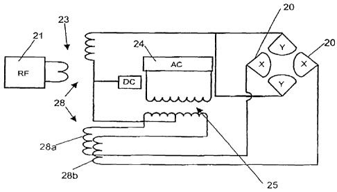
electrodes. Figure 3 shows the conceptual schematic of a conventional
apparatus for applying the
RF and AC voltages to a two-dimensional quadrupole electrode structure. In
this example, the
rod electrodes are not divided into segments, therefore simplifying our
example. However, the
basic schemes for applying the RF and AC voltages to the electrodes does not
change if the rod
electrodes are segmented. Figure 3 indicates how the X electrode pair AC
voltages are combined
with the X electrode RF voltage. The RF voltage source 21 drives the primary
winding of the
tuned circuit RF transformer 22 to produce the X and Y rod high RF voltages at
the end
connection points of secondary winding 22 of tuned circuit RF transformer 23.
The AC voltage
source 24 drives the primary winding of AC transformer 25 producing a
differential AC voltage
across the center tapped secondary winding of AC transformer 25. The high X
rod RF voltage
connection point of the secondary winding 22 of the RF transformer is
connected to the center
tap of the secondary winding of AC transformer 26 to add the desired of high X
rod RF voltage
to the opposing phases of AC voltages produced at the ends of the secondary
winding of the AC
transformer. The opposing ends of the AC transformer 26 secondary winding are
connected
correspondingly opposing X rod electrodes and the high Y rod voltage
connection point of the
RF transformer 23 is connected to both Y rod electrodes. The design
requirements for the
broadband transformer AC coupling transformer 26 are such that it needs to
provide reasonably
uniform AC voltage coupling and transformation between its primary and
secondary windings
over a wide frequency range (about 10 kHz to beyond 500 kHz, assuming ci = 27r
x 1,000 kHz).
If broadband multi-frequency AC waveforms are to be used, the amplitude of the
voltage across
the transformer secondary, 2VAUX , may exceed 150 volts. Although this
approach has been
successfully used, in many cases a major disadvantage of this approach is that
the primary input
of the AC transformer 26 is near "ground" potential and the secondary is
floated at the RF
voltage. Consequently, the primary and secondary windings to the broadband AC
transformer
must be sufficiently insulated such that the maximum RF voltage applied to the
electrodes,
VRF MAXIMUM, can be withstood without voltage breakdown or significant RF
power dissipation
in the transformer. For a high performance/ high voltage system, VRF MAXIMUM
may approach
-6-
CA 02474862 2010-09-24
52675-4
5,000 volts. All of this RF voltage is dropped between the primary and the
secondary windings
of the AC transformer
The bandwidth and output voltage requirements for the broadband AC transformer
may
readily be met using a conventional transmission line type transformer wound
on a high
permeability toroidal ferrite core and which has modest size (about
2"x2"xl.5"). The additional
constraint of having very high RF voltage isolation between the primary and
secondary windings
greatly complicates the design of such a device and requires a much larger and
slhbstantially more
expensive AC transformer design.
Objects and Summary of the Invention
It is an object of the present invention to provide an improved circuit for
applying
combinations of AC and RF voltages to the electrodes of quadrupole field
devices such as two-
and three-dimensional RF quadrupole ion traps and two-dimensional mass
filters.
It is a further object of the present invention to provide a circuit for
applying
combinations of AC, RF and DC voltages to quadrupole field devices which
overcomes the
problems associated with coupling of AC voltages to the RF and DC voltages
encountered in the
prior art.
It is another object of the present invention to provide a circuit for
coupling auxiliary AC
voltages on to RF voltages which avoids the problems of coupling with a
broadband transformer
based scheme of the prior art.
There is provided a circuit for applying RF and AC voltages to the rods or
electrodes of
an ion trap or guide comprising an RF transformer having a primary winding and
a secondary
winding having at least two filars, said secondary winding having a lower RF
voltage at one
connection point (tap) than at other connection points (output taps), a first
AC transformer
having a primary winding and a secondary winding, the ends of said secondary
winding each
connected to separate filars at the low voltage connection point of the RF
transformer secondary
winding, a second AC transformer having a primary winding with its ends
connected to the other
end of said filars at the high voltage connection point of said RF transformer
secondary winding
and a (AC) secondary winding having its ends adapted to connect to
electrically isolated
electrodes of said ion trap or guide whereby combined RF and AC voltages are
applied to the
electrodes.
-7-
CA 02474862 2010-09-24
52675-4
An aspect of the invention provides a circuit for applying RF and AC
voltages to electrodes of a RF inhomogeneous field device comprising: an RF
transformer having a primary winding, and a secondary winding coupled to said
primary winding, said secondary winding having at least two electrically
isolated
filars upon which RF voltage couples substantially identically, and said
secondary
winding having a low RF voltage connection point and a high RF voltage
connection point, a source of AC voltage connected between said at least two
filars of the RF secondary windings at the low-voltage connection point of
said RF
winding, said filars supplying the combined RF and AC voltages to at least one
electrode of the inhomogeneous RF field device.
Another aspect of the invention provides a circuit for applying RF
and AC voltages to a linear multipole device of the type having at least two
pairs
of opposing linear rod electrodes comprising: a RF transformer having a
primary
winding adapted to be connected to a source of RF voltage, a secondary winding
coupled to said primary winding, said secondary winding comprising a first
section
having at least two filars, and said secondary winding having a low-voltage
end
and a high-voltage end, a second section having a low-voltage end adapted to
be
connected to the low-voltage end of one of said filars, and a high-voltage end
adapted to be connected to one pair of said electrodes to apply RF voltage
thereto, and an AC transformer adapted to be connected to an AC voltage
supply,
and the output of said AC transformer adapted to be connected between two
filars
of the first section of said secondary winding of the RF transformer at the
low-voltage end, the high-voltage end of said two filars supplying a
differential AC
voltage between and a common RF voltage to at least one pair of said
electrodes.
Still another aspect of the invention provides a circuit for driving
electrodes of a linear quadrupole ion trap of the type having a center section
and
two end sections, each including two pairs of spaced electrodes comprising: a
RF
transformer having a primary winding adapted to be connected to a source of RF
voltage and adapted to be a center-tapped secondary multi-filar winding
coupled
to said primary winding, said secondary winding comprising a first section
having
at least three filars having a low-voltage connection point and a high-voltage
connection point, and a second section having at least three filars which have
a
-7a-
CA 02474862 2010-09-24
52675-4
low-voltage end adapted to be connected to corresponding filars at the low-
voltage connection point of the first section and a high-voltage connection
point,
each filar adapted to be connected to one pair of each of said electrodes in
each
of said center and two end sections to apply RF voltage to said electrodes, a
broadband transformer connected to apply AC voltage between two filars of the
first winding section at the low-voltage connection point of said winding, an
output
broadband transformer having a primary winding connected to the high voltage
connection point of said two filars of the first section, a third AC
transformer,
having a primary winding for receiving the output of said output broadband
transformer, and three secondary windings, each one connected between one pair
of the spaced electrodes of each of said center and two end sections for
applying
RF and AC voltages thereto.
A further aspect of the invention provides a circuit for driving
electrodes of a RF quadrupole linear ion trap of the type having at least a
center
section and two end sections, each including two pairs of spaced electrodes
comprising: an RF transformer having a primary winding adapted to be connected
to a source of RF voltage and a multi-filar center-tapped secondary winding
coupled to said primary winding, said secondary winding comprising a first
section
having at least three filars having a low-voltage end and a high-voltage end,
and a
second section having at least three filars which have a low-voltage end
connected to the low-voltage end of the first section and a high-voltage end,
each
filar adapted to be connected to each of said center and two end sections in
one
pair of each of said electrodes; a broadband transformer connected to apply AC
voltage between two filars of the first winding section at the low-voltage end
of
said windings; and output broadband transformer means connected to said two
filars at the high voltage end of said first section to apply RF and AC
voltages to
the other pair of each of said electrodes in each of said center and two end
sections.
-7b-
CA 02474862 2004-08-03
WO 2003/067627 PCT/US2003/003495
Brief Description of the Drawings
Figure 1 is a representation of a linear quadrupole ion trap;
Figures 2a-2c illustrate the DC, AC and RF voltages necessary for operation of
the two-
dimensional ion trap shown in Figure 1;
Figure 3 schematically shows a prior art circuit for applying RF and AC
voltages to the
electrodes of an ion trap;
Figure 4a schematically shows a conceptual embodiment of the invention for
combining
an AC voltage to an RF drive voltage to drive the X rod;
Figure 4b schematically shows another conceptual embodiment of the invention
for
combining an AC voltage to an RF drive voltage to drive the X rod;
Figure 5 is a schematic diagram of yet a further conceptual embodiment of the
invention
for combining an AC voltage to an RF drive voltage to drive the X rod;
Figure 6 is a detailed circuit diagram of the circuit according to Figure 5;
Figure 7 schematically shows circuit diagram of still a further conceptual
embodiment
configured to drive the segment rods of a segmented quadrupole structure;
Figure 8 is a detailed circuit diagram of the circuit according to Figure 7;
Figure 9 is an embodiment of the invention in which separate auxiliary
voltages are
coupled to the X and Y rod electrodes of a segmented quadrupole electrode
structure;
Figure 10 is a schematic diagram of a three-dimensional ion trap having a
segmented ring
electrode;
Figure 11 is a schematic circuit diagram of an embodiment of the invention for
applying
dipole voltages to the segments of the ring electrode; and
Figure 12 is a schematic diagram of another circuit incorporating the present
invention for
driving the electrodes of a segmented two-dimensional ion trap such that an
auxiliary AC
quadrupole field is superposed on the main RF quadrupole field.
Description of Preferred Embodiments
A brief discussion of the design and construction of RF tuned transformers 23
is helpful
in the understanding of the present invention. The reason that such devices
are used is that it is
possible to generate high RF voltages in the frequency range needed for RF
quadrupole/multipole
devices with relatively modest amounts of RF power. The secondary winding of
the transformer
is, in essence, a very large air cored solenoidal inductor. The connection of
the secondary
-8-
CA 02474862 2004-08-03
WO 2003/067627 PCT/US2003/003495
winding to the rod electrodes puts an almost purely capacitive reactance
across this inductor
creating an LC resonant circuit. Since there is essentially no resistive
component to this load the
only source of damping is the resistance of the wire in the coil windings and
resistive losses
associated with induced currents in the circuit enclosure. Hence this LC
circuit has a very high
quality factor, Q, and a correspondingly narrow resonant bandwidth. A basic
characteristic of
such circuits is that if you drive them within their resonant band they
produce a large voltage
response. It is this property which is utilized to create a very efficient
means of RF voltage
transformation. The primary of the transformer 23 in Figure 3 is simply a few
isolated turns
wrapped around the center region of the solenoidal secondary windings or
alternatively
interspersed between turns of the secondary solenoid in the central region of
the coil. When a RF
voltage at the resonant frequency of the tuned circuit is applied to the
primary winding of the
transformer, inductive coupling drives the secondary winding of the
transformer and a much
larger RF voltage develops across this winding. Resonant transformers allow
voltage
transformation ratios (VRF-SECONDARY /RF_PRIMARY) of well greater than 100.
Such voltage
transformation ratios are not feasible using conventional broadband ferrite
cored RF
transformers. The quality factors, Qs, for the tuned circuit transformers used
on high
performance mass spectrometers may approach or exceed 200. This enables
generation of RF
voltages, 2VRF, of greater than 10,000 volts with RF power amplifiers that
deliver less than 100
watts of RF power. This is necessary in order to construct high voltage/high
performance RF
quadrupole field mass spectrometers having acceptable size, power consumption
and cost.
Multi-filar tuned circuit transformer coils may be constructed in many ways,
for example:
on helically grooved poloycarbonate tube coils, the individual filars wound
against each other to
create a single multifilar wire bundle in the grooves of the coil form; by
winding a custom made
twisted mutli-filar wire bundle onto a helically grooved coil form; by using
mutli-stranded braid
of magnet wires or some other wires with thin insulation; or by using very
thin coaxial cable.
While using a helically grooved coil form is convenient for hand winding
coils, smooth tubes or
arrays of rods made of material that does not absorb RF power could also be
used. The examples
given above are considered exemplary and other alternative constructions may
be employed in
practicing the current invention.
The invention will first be described with reference to the conceptual
schematics of
Figures 4a, 4b, and 5. It should be noted that Figure 4a, 4b and 5 show only
those apparatus
components which are the most important to illustrate the invention. Those
skilled in the art will
be familiar with other required or optional components, which therefore do not
need to be
-9-
CA 02474862 2004-08-03
WO 2003/067627 PCT/US2003/003495
particularly illustrated or mentioned. In addition, it will be appreciated
that although DC
supplies are illustrated throughout the current invention, these may, if
applicable, be replaced by
DC "ground" connections.
Figure 4a illustrates an embodiment of the invention, in which the problems of
coupling
the AC at the high voltage side of the RF transformer 23 are avoided by
coupling the AC at the
low voltage connection point of the RF transformer/coil. This configuration
requires the use of
multiple filars or windings 28 on the main RF coil with the AC voltage being
applied across two
filars 28a, 28b. As illustrated, and preferably, a broadband transformer 25
couples the AC supply
voltage across the two filars 28a, 28b. This method of coupling the AC voltage
on to the filars
does not interfere with flow of RF current through the RF transformer
secondary. Other
equivalent methods of coupling are feasible and known to those skilled in the
art. This particular
embodiment has limitations because the AC supply must now drive the ion trap
electrode load
through the distance of the secondary windings of the RF coil. The filar
windings 28a, 28b of the
RF tuned transformer generally constitute a low characteristic impedance
(under 10012) two wire
transmission line. The combination of a large miss-match between the largely
reactive
(capacitive) terminating impendence and the preferred terminating impedance of
the windings
28a, 28b will likely cause a substantial non-uniformity in the propagation of
the higher frequency
components in the AC supply waveform voltage through the RF coil windings.
Load resistors of
appropriate value could placed across the connections to the X electrodes 20
so as to swamp the
capacitive load they present to the AC circuit and provide the appropriate
terminating impedance.
This would greatly improve the uniformity of the frequency response of the AC
over the desired
bandwith. However the power required to drive such a low load impedance limits
the amplitude
of the AC voltage actually imposed between the X electrodes 20 to values too
small for when
broadband frequency waveforms are required, as broadband waveform applications
require
higher AC voltage amplitudes in order to get adequate power into all frequency
components
necessary for ion ejection.
A second alternative arrangement which similarly avoids the problems of
coupling at the
high voltage side of the RF transformer is illustrated in figure 4b. This
arrangement again
introduces DC 27 and AC 34 voltages on to the low voltage connection point 31
of the multi-filar
transformer section 32 of RF transformer 33. Again, these voltages are
transferred through the
RF transformer section 32 to the high voltage side of the RF transformer
section 32 and an AC
voltage is transmitted to the primary 35 of an AC broadband transformer 36 via
filars 37 and 38.
The DC 27 is transmitted through to a center tap 29 on the secondary of the AC
transformer 36
-10-
CA 02474862 2004-08-03
WO 2003/067627 PCT/US2003/003495
through filars 32. This approach also can create a large miss-match between
the terminating
impendence and the preferred terminating impedance of the RF coil winding
filars 37 and 38
which may cause a substantial non-uniformity in the propagation of the higher
frequency
components in the AC supply waveform voltage through the coil windings. Again,
load resistors
of appropriate value could placed across the connections to the X electrodes
20 so as to swamp
the capacitive load they present to the AC circuit and provide the appropriate
terminating
impedance. However utilization of the transformer 36 as an impedance
transformer allows use of
much higher load resistances between the X electrode connections and while
still presenting an
appropriately low terminating impedance at the high RF voltage ends of filars
37 and 38. This
then allows much higher AC voltages to be imposed between the X electrodes 20
for a given
amount of AC power dissipated.
A preferred arrangement which avoids the problems of coupling at the high
voltage side
of the RF transformer and the impedance matching issues is illustrated in
Figure 5. This
arrangement introduces the DC 27 and the AC 34 voltages into the low voltage
side 31 of the
multi-filar transformer section 32 of RF transformer 33. As illustrated, and
preferably, a
broadband transformer 25 both voltage transforms the AC supply voltage and
couples it across
the two filars 37 and 38 at the low voltage connection point of the x side of
the tuned RF
transformer coil 32. The resulting AC voltage output by this first AC
transformer 25 is then
transferred through the RF transformer 33 to the high voltage side of the RF
transformer 33 via
filars 37 and 38. Preferably, the AC voltage is further transformed after
transmitting to the RF
high voltage end of the X side of the RF coil 32 by a second broadband AC
transformer. The
high voltage ends of filars 37 and 38 drive the primary 35 of the AC broadband
transformer 36.
This configuration again allows the use of relatively high valued resistors
30a and 30b, across the
X electrodes 20 while still properly terminating the transmission line
comprised of filars 37 and
38, thus allowing for uniformity in the propagation of the higher frequency
components in the
AC supply waveform voltage through the RF coil secondary winding. The
introduction of
voltage transformation or voltage gain though the first AC transformer 25
allows the AC voltage
source 34 to drive an impedance other than that which is presented at the low
RF voltage
connection to filars 37 and 38. This increases the ratio between the amplitude
of the AC voltage
applied between the X electrodes and that output by the AC voltage source 34
thus reducing the
required maximum voltage that the AC voltage source 34 needs to deliver.
A detailed description of the conceptual embodiment illustrated by Figure 5
now follows.
Referring to Figure 6, the X side of the secondary of the tuned RF transformer
33 is used as the
-11-
CA 02474862 2004-08-03
WO 2003/067627 PCT/US2003/003495
means for combining the auxiliary AC voltage and the RF voltage. A low voltage
reference
version of the desired AC voltage waveform is generated by an auxiliary AC
synthesizer 42.
This low voltage AC waveform is in turn amplified with a broadband amplifier
43. The output
of this amplifier drives the primary 44 of an AC broadband transformer 46.
However, the
secondary 47 of this AC broadband transformer is not connected to the high RF
voltage end of
the X side of RF tuned circuit transformer secondary. Instead it is connected
to the low RF
voltage end of the X side of the RF tuned circuit transformer secondary. The X
side of the RF
tuned circuit transformer secondary is now constructed as a tri-filar winding
with the windings
labeled A, B and C, so as to create three identical but insulated X side
windings that substantially
behave in terms of the RF circuit as one winding. The ends of the secondary 47
of broadband
transformer 46 are connected to the A and C filars of the X side of the RF
transformer secondary
at the low RF voltage connection point (end). The center tap of the secondary
of broadband
transformer 46 is connected to both the B filar of the low voltage end of the
X side of the RF
transformer secondary and the low voltage connection point (end) of the Y side
of the RF
transformer secondary. Thus a differential version of the AC voltage waveform
is imposed
between the A and C filars, with the B filar acting as a sort of AC "ground".
The center tap of
the secondary of broadband transformer 46 is also the place where the DC
offset voltage is
connected to the circuit, thus DC biasing all of the secondaries of the tuned
RF transformer. This
point is maintained near RF "ground" by connecting it to ground through a
bypass capacitor,
CBYPASS. The value of CBYPASS needs to be chosen such that it is large enough
so that its
reactance is small in comparison to the reactance of the RF tuned transformer
secondary, and yet
not so large that it detrimentally effects the rate at which the DC bias
voltage can be changed
during an experiment. This means that CBYPASS is typically on the order 5,000-
10,000 pF.
Depending on the specific physical implementation of the circuit, a CBYPASS
may be unnecessary.
The RF currents flowing in the A and C filars of the X side of the secondary
of the RF tuned
circuit transformer will be nearly identical, therefore the secondary windings
of broadband
transformer 46 will present a negligible reactance for these currents. Thus,
at the low voltage end
of the X side of the secondary of the RF tuned circuit transformer, all three
filars will be
maintained near RF "ground". Since the three filars of the X side of the RF
tuned circuit
secondary winding are essentially identical, RF voltage is equally coupled on
to them. Thus, at
the high end of the X side of the RF tuned circuit, all three filars have the
same RF voltage, VRF ,
and DC voltage, VDC but differing AC voltages. The A and C filars drive the
ends of the primary
winding of a second broadband AC transformer 48. The ends of the secondary
winding of
-12-
CA 02474862 2004-08-03
WO 2003/067627 PCT/US2003/003495
broadband transformer 48 are in turn connected to X1 and X2 rod electrodes
thus applying the
final voltage transformed version of the AC voltage waveform, 2VAUx(t),
between the rod
electrodes. To provide the appropriate load impedance, a pair of identically
valued load resisters,
RL, which are connected in series are also connected across the ends of the
secondary of
broadband transformer 48. The B filar of the X side of the RF tuned circuit
secondary is
connected to the center taps of both the primary and secondary windings of
broadband
transformer 48, and the interconnection point between the two load resistors.
This circuit node
corresponds to an AC "ground" which is "floating" on the combined RF and DC
voltage,
VRFCos(Wt) + VDC. This makes it the ideal place to sample the RF voltage
amplitude. A
connection is therefore made from this node to the RF detection circuitry
through a precision RF
detector capacitor, CDET. This "floating" AC ground arrangement also insures
that the AC
voltages applied to the X1 and X2 rod electrodes are the equal and opposite
voltages
corresponding to VAUX(t) and -VAUX(t) which are required to generate the
desired dipole auxiliary
field.
Broadband transformer 48 is necessitated by the requirement that the maximum
amplitude of VAUx(t) be allowed to exceed 100 volts and the fact that the tri-
filar X winding of
the RF tuned transformer constitutes a low characteristic impedance (under 20
]) three wire
transmission line (a pair of differentially driven wires and shield wire). The
length of the X
windings may easily be on the order of 30 meters. Depending on the dielectric
constant of the
insulation between filars, such a length could easily be on the order of 1/8
of a wavelength for
frequencies in the upper end of the bandwidth of the auxiliary voltage
waveform. A large miss-
match between the terminating impendence (load resistance) and the
characteristic impedance of
the X winding three wire transmission line would cause a substantial non-
uniformity in the
propagation of the higher frequency components in the auxiliary waveform
voltage through the
coil winding. As the DC resistance of the individual filars are on the order
of 6 I, terminating
this transmission line at its characteristic impedance is also undesirable as
it would result in an
unacceptable attenuation in the AC waveform voltage during its transmission to
the high RF
voltage end of the winding. Fortunately, since the frequency band of interest
only barely extends
into the domain where these effects are significant, adequate uniformity of
frequency response
and acceptable attenuations can be obtained with a terminating impedance of
about 50-60 Q.
Broadband transformer 48 provides the necessary impedance matching between the
desired 50-
60 SZ terminating impedance for X winding transmission line and a sufficiently
high load
-13-
CA 02474862 2004-08-03
WO 2003/067627 PCT/US2003/003495
impedance such that a modest amount of AC power will be required to generate
the desired
maximum auxiliary voltage waveform amplitudes. Transformation ratios of 2/1,
3/1 and 4/1
(corresponding to impedance transform ratios of 4/1, 9/1 and 16/1) are readily
achieved if
broadband transformer 48 is constructed as a conventional high permeability
ferrite cored
transmission line transformer. Such transformers are relatively small (ca.
2"x2"xl.5") and are
not expensive to construct. Since the entire transformer is "floated" at VRF,
there is neither the
voltage isolation problem nor the added capacitance problem associated with
the broadband
coupling transformer of the prior art. Assuming a 50 J terminating impedance
and a 3/1 voltage
transformation ratio with broadband transformer 48, application of a 100 Volt
auxiliary voltage
between the Xl and X2 rod electrodes will result in a dissipation of about 11
watts of power in
the load resistors. This is very manageable in regards to both power
dissipation in the circuitry
and the size and cost of the AC amplifier needed to deliver this power. It
should also be noted
that if the AC Amplifier is able to drive low impedances, the broadband
transformer 36 may be
wound to provide impedance matching and voltage transformation (boost) at the
input end of the
X winding transmission line. In some applications no DC voltage may be
required, so a DC
"ground" may be substituted for it. In some case adequate performance may be
obtained without
the use of the AC "ground" filar, B.
To this point the discussion of the prior art and the invention have been
limited to the
case where the rod electrodes have a single segment, as would be the case for
a mass filter or
linear ion trap with plate lenses adjacent to the rod ends which are biased to
provide the axial
trapping field. However, the invention can be readily adapted to the case
where the rod
electrodes are divided into segments. Figure 7 shows schematically a
conceptual embodiment of
the invention whereby the appropriate superpositions of the auxiliary AC, RF
and DC voltages
are generated for a linear quadrupole trap whose rod electrodes are divided
into three segments.
The circuit includes an RF air core transformer 33 having a primary winding,
and a multi-filar
secondary winding. As depicted in Figure 7, the X side of the RF transformer
secondary winding
comprises five filars 56, 57, 51a, 52a, and 53a. The Y side of the RF
transformer secondary
winding of the RF transformer is comprised of three filars 5lb, 52b, 53b. The
RF transformer's
center tap is near RF "ground" and the filars joined at the center tap, 51a,
51b; 52a, 52b; 53a, 53b
are connected to the DC voltages DC1, DC2, DC3 respectively. The other
connection points, the
ends of the RF transformer secondary winding, are at high RF voltage generated
for application
to the X and Y rod segments to provide the trapping fields. The AC or
excitation voltage is
-14-
CA 02474862 2004-08-03
WO 2003/067627 PCT/US2003/003495
coupled between the low RF voltage connection points of the X side RF
transformer secondary
winding filars 56 and 57 by a first AC transformer 46. The high voltage
connection points of
the RF transformer X side filars 56 and 57 are connected to the primary
windings of a second AC
transformer 48 which has center tapped identical secondary windings 61, 62 and
63. The high
voltage connection points of the X side RF transformer secondary winding
filars 51a, 52a, 53a
are connected to the center taps of this 2nd AC transformer's secondary
windings, 61, 62, and 63,
respectively and thus also DC biasing them with voltages DCl, DC2 and DC3
respectively. The
ends of this second AC transformer's secondary windings 61, 62, 63 are
connected across the X
rod segment pairs X1F, X2F; X1CX2C; and X1B, X2B, respectively. The ends of
the Y side of
the RF transformer secondary winding filars 5 lb,52b, and 53b connect to the
YF,YC and YB rod
electrode segment pairs respectively. The corresponding secondary winding ends
of the second
AC transformer are connected to segments of the same multi-segment X rod,
thereby insuring
that the same a AC voltage phase is applied to all segments of each multi-
segment X rod and that
the opposing X rods have equal amplitude and opposite phase AC voltages
imposed on them.
The opposing ends of each secondary winding of the second AC transformer are
connected to
opposing segments of the X rods. The filar connected to each center taps of
each second
transformer secondary winding corresponds the Y filar connected to the Y rod
segments adjacent
to the X rod segments connected to the ends of the same second transformer
secondary. Thus all
the rod segments of each section of the structure are biased at the same DC
offset potential. All
windings of the second transformer are "floated" at a common high RF voltage
and phase thus
imposing the same RF voltage to all X rod segments. Since all filars emanating
from the high
voltage end of the Y side of the RF transformer have a common RF voltage
(opposite in phase
and nearly identical in amplitude from those emanating from the high voltage
end of the X side
of the RF transformer secondary), a RF voltage opposite in phase and nearly
equal in amplitude
to that imposed on the X rods is imposed on the Y rods. Thus all of the
desired DC, AC and RF
voltage superpositions are created and imposed on the 12 electrode segments of
a three segment
linear quadrupole trap.
A detailed description of the conceptual embodiment illustrated by Figure 7
now follows.
Referring to Figure 8, the number of filars comprising the secondary winding
of the RF tuned
circuit transformer have been increased to six and are labeled A, B, C, D, E,
F. On the X side of
the transformer, the A, B, and C filars correspond in function to the filars
A, B, and C in Figure
6. The AC amplifier (not shown) again drives the primary winding of a first
broadband AC
transformer 46. As before, the ends of the secondary winding of broadband
transformer 46 are
-15-
CA 02474862 2004-08-03
WO 2003/067627 PCT/US2003/003495
connected to the A, and C filars of the X side of the RF tuned circuit
secondary at its low voltage
end (center tap). Also as before, the center tap of the broadband transformer
46 is connected to
the B filar of X side of the RF tuned circuit secondary at its low voltage
connection point (center
tap). However, in the depicted implementation, the center tap of the broadband
transformer 46 is
connected to ground rather than a DC bias voltage. Thus the A, B and C filars
on the X side of
the tuned circuit transformer coil are all biased at DC "ground" potential.
The A, B, and C filars
of the Y side of the RF tuned circuit transformer coil secondary are also tied
to DC "ground".
The DC offset voltages for the Front, Center and Back rod electrode sections
are fed through RF
blocking filters 66, 67 and 68 to bias the D, E and F filars of both the X and
Y sides of the RF
tuned circuit transformer secondary winding at the low voltage point of the
secondary winding
(center tap). To insure that the low voltage ends of the RF tuned transformer
secondary halves
are maintained close to RF "ground", the D, E and F filars are connected to
ground though
bypass capacitors 69. Just as before, at the high voltage end of the X side of
the RF tuned circuit
secondary, the A, and B filars drive the primary winding of second AC
broadband transformer
48. Again, the B filar connects to the center taps of both the primary and the
secondary of this
second broadband transformer 48. At the high voltage ends of this
transformer's secondary
windings the B filar also serves as the feed-back source for the RF voltage
amplitude regulation
servo loop and therefore is connected to the RF detector circuit though a
precision capacitor,
CDET. This second broadband transformer 48 serves as a voltage/ impedance
transformer whose
outputs feed the primary winding of a third AC broadband transformer 71.
Transformer 71 is
used to couple the auxiliary voltage generated at the outputs broadband
transformer 48 on to the
DC offset voltages carried by the D, E and F filars. Transformer 71 has three
identical secondary
windings 72, and the fully transformed auxiliary voltage is coupled
identically on to all of them.
The center taps of these three secondary windings are each driven by one of
the DC voltage
carrying filars (D, E and F). The desired superpositions of the RF, AC and DC
voltages appear at
the ends of these secondaries. The transformer secondary windings 72 are
connected to the
appropriate rod electrode segments as indicated in the drawings. A pair of
load resistors RL are
connected across each of the three secondaries 72 of broadband transformer 71
to provide
uniformity of amplitude response with frequency. Since both the primaries and
secondaries of
these two broadband transformers 48, 71 are floated at high RF voltage, there
are none of the
voltage isolation problems associated with the prior art approach. While,
conceivably, the
functions of broadband transformer 71 and broadband transformer 48 could be
combined in one
transformer it is preferred to attain the desired functions of voltage
transformation and AC to DC
-16-
CA 02474862 2004-08-03
WO 2003/067627 PCT/US2003/003495
coupling with two transformers wound on separate ferrite cores.
On the high voltage end the Y side of the RF transformer, the D, E, and F
filars are
connected directly to the appropriate Y rod electrode segments as they already
have the desired
superpositions of RF and DC voltage. Also at the high voltage end of the Y
side of the coil, the
A, B, C filars are connected together and to the Y side RF detector capacitor
to provide feedback
of the Y electrode RF voltage amplitude to the RF voltage amplitude control
loop. On the Y side
of the tuned RF transformer the A, B and C filars could be replaced by a
single filar. However,
from a manufacturing standpoint it would probably be easier to use the same
multi-filar wire on
both sides of the RF transformers secondary winding.
The schemes for generating the necessary superpositions of RF, DC and AC
voltages for
a three segment two-dimensional RF quadrupole ion trap illustrated in Figures
7 and 8 can be
extended or modified in various other ways. One simple extension of this
design would be the
case where the trap is divided into four segments. The expedient way of
modifying the circuitry
to accommodate the extra segment would be to disconnect the ground connection
of the B filar of
the RF tuned transformer secondary winding and drive it with an additional DC
voltage supply
through an additional filter and then simply connect the primary connections
of broadband
transformer 71 to the added segments of the X1 and X2 rods. Alternatively, a
seventh filar could
be added to the RF tuned transformer secondary winding with a corresponding
secondary
winding added to broadband transformer 71.
Another very likely extension to the scheme shown in Figure 8 would be the
case where a
second independent dipole field oriented in the Y dimension is also desired.
This can be
straightforwardly accomplished by making the circuitry on the Y sides of the
RF tuned
transformer secondary winding a replicate of that on the X side of the
winding. Figure 9 shows
one way this may be accomplished. The same DC supplies and filters 66, 67, 68
are used for
both X and Y sides of the RF transformer coil as the X and Y rods in each
segment are equally
biased. However, this is not inherent to the invention, certainly separate and
different DC
voltages may be applied to the X and Y rod electrode in any particular
segment. There are
dedicated X and Y auxiliary waveform AC amplifiers, broadband transformers 46,
46a,
broadband transformers 48a, 48b, and broadband transformers 71a, 71b and
associated load
resistors 72a, 72b. The function of the subunits remain unchanged.
A different application of the invention would be the case were different
auxiliary
voltages would need to be applied to segments of the same electrode and
therefore need to be
combined with the same high RF voltage. One example of where one would want to
do this is
-17-
CA 02474862 2004-08-03
WO 2003/067627 PCT/US2003/003495
when one wants to independently excite the x and y dimensional modes of
oscillation (radial
modes) of trapped ions within a three-dimensional RF quadrupole ion trap of
the type having end
caps 51 and 52 and a ring electrode 53, Figure 10. This would entail the
superposition of
separate dipole fields respectively polarized in the x and y dimensions on to
the main three-
dimensional RF quadrupolar trapping field. Since in these devices, ions from
an external source
or ionizing electrons are typically introduced through one of the end cap
electrodes, the RF
voltage, VRFCOS(wt), is typically applied to only the ring electrode. Both the
end cap and ring
electrodes are biased at a common DC potential, VDC. One approach to
accomplishing the
superposition of the two auxiliary fields in an ion trap in accordance to the
invention is shown
schematically in Figure 10. The ring electrode 53 is divided into four equal
and electrically
isolated segments. These segments are designated in clockwise order as Y1, X1,
Y2 and X2.
The same RF voltage, VRFC0s(wt), is applied to all of the ring electrode
segments. To create
approximate x and y polarized auxiliary dipole fields, voltages 2VAUx-x(t) and
2VAUx-y(t) are
applied differentially between the corresponding opposing segments of the ring
electrode. Below
are listed the voltages applied to each segment of the ring electrode.
Ring Electrode Segment Voltage
X1 Vx1= VRFCOS(wt) + VDC + VAUX X(t)
X2 VX2 = VRFCOS(wt) + VDC - VAUX x(t)
Y1 VY1 = VRFCOS(wt) + VDC + VAUX Y(t)
Y2 VY2 = VRFCOS(wt) + VDC - VAUX-Y(t)
A suitable circuit for applying RF, AC and DC voltages to the Ring electrode
segments is shown
in Figure 11. Since the RF voltage is applied only to the Ring electrode, the
secondary winding
of the multi-filar tuned circuit RF transformer 76 is a continuous winding and
not divided into
halves. It is constructed as a five filar winding. Filars A and B carry the x
dimension auxiliary
AC power and filars D and E carry the y dimension auxiliary AC power. The C
filar corresponds
to the AC "ground" for these auxiliary voltages. As before, the auxiliary
voltages are coupled on
to filars of the secondary winding of the tuned RF transformer at the low RF
voltage end (tap) of
the winding by broadband transformers. Broadband transformer 77 couples the X
AC voltage
between filars A and B and broadband transformer 78 couple the Y AC voltage
between filars D
and E. Center taps of the secondaries of these two transformers 77,78 are
connected together,
-18-
CA 02474862 2004-08-03
WO 2003/067627 PCT/US2003/003495
and to the C filar of the RF transformer secondary winding. The DC voltage to
bias the ring
electrode (DC offset voltage) is brought through a RF blocking filter and is
also connected to the
center taps of these broadband transformers thus biasing all the filars of the
RF tuned transformer
secondary winding. The low RF voltage end of the RF tuned transformer
secondary is connected
to system "ground" through a bypass capacitor, CBYPASS. In this case, since
the secondary is only
single sided (rather than differential as in the previously described
embodiments), a considerable
amount of RF voltage will appear on the low voltage side of the RF tuned
transformer secondary.
The magnitude of this voltage is approximately given as VRFXCTRAP/CBYPASS,
where CTRAP is the
capacitance between the ring and end cap electrodes. CTRAP and CBYPASS are
typically on the
order of 50 pF and 5,000 pF respectively. This means that several tens of
volts of RF can appear
at this point. As this RF voltage appears essentially equally at the all
outputs of both broadband
transformers 77 and 78, minimal RF voltage (or power) is coupled across these
transformers and
into the respective AC amplifiers. On the high RF voltage side (connection
point) of the RF
tuned transformer secondary, the A and B filars connect to the primary inputs
of broadband
transformer 79 and the D and E filars connect to the primary inputs of
broadband transformer 81.
The C filar connects to the center tap inputs of both of these transformers.
The C filar also
provides the feedback for the RF voltage amplitude control loop as it is
connected to the RF
detector circuitry though a RF detector capacitor, CDET. The outputs of
broadband transformer 79
and broadband transformer 81 are connected to the X1, X2 and Y1,Y2 ring
electrode segment
pairs. As before, a pair of load resistors RL are connected in series across
the outputs of these
transformers with their connection point connected to the center tap of the
transformer. In this
embodiment the broadband transformer 58 and broadband transformer 59 are
configured as auto-
transformers. This illustrates that there is not just one way to construct the
transformers to
accomplish the desired AC voltage/impedance transformation.
The previously described embodiments of the invention have been directed to
creating the
necessary voltage combinations for superposing dipolar AC auxiliary fields
upon RF quadrupole
field devices. The invention is in no way restricted to the superposition of
AC dipole fields on to
RF quadrupole fields. Figure 12 shows an embodiment of the invention which
produces the
necessary voltage combinations to superpose an auxiliary AC quadrupole field
on the RF
quadrupole field of a three segment two-dimensional quadrupole ion trap. The
circuit in Figure
12 is identical to that of Figure 8 and bears the same reference numbers
except in the terminating
connections to the various rod segments. Only one terminal 81 of each
secondary winding of
-19-
CA 02474862 2004-08-03
WO 2003/067627 PCT/US2003/003495
broadband transformer 71 is connected to the corresponding device segment of
both the X1 and
X2 rod electrodes. The other terminal 82 of each secondary winding is
connected to balancing
capacitors whose other terminals are connected to "ground". These are denoted
as CxF, Cxc, and
CXR. These capacitors insure that a balanced amount of RF current flows
through each side of
each secondary winding 72 of broadband transformer 71 resulting in no net
magnetization of the
transformer core. Thus broadband transformer secondary windings 72 present a
near zero
impedance for RF currents and therefore the AC circuit load resistors RL are
removed from the
RF current path. This added capacitance on the X side of the RF tuned
transformer resonant
circuit is matched by adding corresponding amount capacitance on the Y side of
the RF tuned
transformer circuit in order to maintain the symmetry of the RF voltages on
the X and Y rod
electrodes. This balancing capacitance to "ground" is provided by CYF, CYM,
and CYR . These
added capacitances do increase the resonating capacitance of the RF tuned
circuit making it less
power efficient. However, in practice, acceptable performance has been
obtained with such a
circuit without using any of the balancing capacitors. This is probably due to
the substantial
amount of capacitance between the primary and secondary windings of
transmission line type
transformers. This provides alternative RF current paths to the rod electrode
segments that are
not through the load resistors for the auxiliary AC circuit.
In the various example shown above, when multiple DC voltages are involved, a
tuned
RF voltage transformer filar is dedicated for each DC voltage and separate
filars are used for the
AC voltage. It should be noted that with additional circuitry and different
transformers at the low
voltage and high voltage ends of the RF tuned transformer it is feasible that
the AC and DC
voltages could be carried on the same filars. This would allow a 3 filar RF
tuned circuit
transformer to supply the three DC voltages and auxiliary AC voltages for a
three segment two-
dimensional quadrupole ion trap. Such a design would be in accordance with the
invention.
However, the added complexity of the circuitry at the terminal ends of the RF
transformer coil
would likely outweigh the advantages afforded by having a RF transformer coil
with fewer filars.
It should also be noted that in the above descriptions the RF tuned
transformer is comprised of
separate primary and secondary windings. However in many instances RF tuned
transformers
constructed as auto-transformers (where the primary and secondary windings
partially share
common conductors) would serve equivalently and the use of such transformers
would be wholly
within the scope of the invention.
While the previous examples have been restricted to applications related to
two and three-
dimensional RF quadrupole field devices, the invention is more broadly
applicable and could be
-20-
CA 02474862 2004-08-03
WO 2003/067627 PCT/US2003/003495
used with higher order RF multipole ion guides (hexapole, octopoles), RF ring
traps and various
other RF inhomogeneous field ion trapping, guiding and sorting devices. The
invention is useful
where the superposition of auxiliary AC voltage on potentially high RF
voltages of the
magnitude and frequencies used for these types of apparatuses is required on
at least one
electrode (or electrode segment) of such a device.
The foregoing descriptions of specific embodiments of the present invention
are
presented for the purposes of illustration and description. They are not
intended to be exhaustive
or to limit the invention to the precise forms disclosed; obviously many
modifications and
variations are possible in view of the above teachings. The embodiments were
chosen and
described in order to best explain the principles of the invention and its
practical applications, to
thereby enable others skilled in the art to best utilize the invention and
various embodiments with
various modifications as are suited to the particular use contemplated. It is
intended that the
scope of the invention be defined by the following claims and their
equivalents.
-21-