Note: Descriptions are shown in the official language in which they were submitted.
CA 02487859 2004-11-29
WO 2004/040670 PCT/US2003/017432
Solid oxide electrolyte with ion conductivity enhancement by
dislocation
CROSS REFERENCE
The present invention cross references the concurrently filed
US Application titled "Sub-micron Electrolyte Thin Film on
Nano-Porous Substrate by Oxidation of Metal Film" by Yong-il
Park, Fritz B. Print, Suk-Won Cha, Sang-Joon John Lee & Yuji
Saito, Attorney Docket No. S02-135/US, which is hereby
incorporated by reference.
FIEhD OF INVENTION
The present invention relates generally to electrochemical
devices and methods. More particularly, the present invention
relates to solid oxide ion conducting electrolyte materials
for solid-state ionic devices such as fuel cells and gas
sensors, by the use of dislocation.
BACKGROUND
A fuel cell is an electrochemical device that produces
electrical current from chemical reactions. The fundamental
device includes an ion-conducting electrolyte between two
electrodes, backed by fuel and oxidant flow distributors. A
catalyst on one electrode promotes separation of ions and
1/15
CA 02487859 2004-11-29
WO 2004/040670 PCT/US2003/017432
electrons at the oxidant side. Only the ions conduct through
the electrolyte, and recombine with electrons at the fuel
side. The electrons are conducted through an external
circuit, thus supplying electrical power. Solid oxide fuel
cells have ionic-conducting metal oxide membranes as their
electrolyte layer. The oxygen molecules are split into their
respective electrons and oxygen ions at the airside. The
oxygen ions propagate through the electrolyte membrane and
combine with their electrons and hydrogen molecules into
water. A gas sensor has same basic configuration, and
produces electrical current that depends on difference of gas
concentration.
Fuel cell operation is increasingly efficient where the well-
known electron conductivity of the electrolyte is brought to
a minimum and the well-known ionic conductivity of the
electrolyte is brought to a maximum. At the same time it is
well known that a fuel cell is thermodynamically more
efficient at lower temperatures, with lower entropic losses
resulting in a higher open cell voltage.
Solid oxide fuel cells [SOFC] have a number of advantages:
~ No humidity requirement for ion exchange
~ No water clogging up with generated water
~ No or less noble metal catalyst
~ High CO tolerance
~ Valuable waste heat
However, SOFCs ~s-~e have problems . One of the main problems
' to be overcome is preparation of hermetic seals. With
decreasing operating temperature from 1000°C to 600°C or less,
metal materials can be used for sealing and the problem
becomes manageable. Many efforts have been made to decrease
operating temperature of SOFCs to below 600°C despite a large
2/15
CA 02487859 2004-11-29
WO 2004/040670 PCT/US2003/017432
loss of output power. However, this operating temperature is
still too high for mobile application.
In particular, an electrolyte layer is needed that may be
fabricated in an inexpensive fashion with a configuration
that provides for an efficient fuel cell operation at working
temperatures of generally less than 500 °C. The present
invention addresses also these needs.
SUMMARY
The present invention provides a solid oxide electrolyte thin
film with dislocations, which penetrate (pass through)
electrolyte from a top surface to bottom surface. T he
present invention adopts preferably ion irradiation in
combination with a heat treatment for fabricating electrolyte
thin films. One preferred embodiment of the present
invention is based on:
l.Conventional ion conducting materials, such as, but not
limited to, Yttria stabilized zirconia or doped ceria
prepared as an electrolyte.
2 .Dislocations that are introduced into electrolyte
materials, preferably by the use of high-energy electron
irradiation and/or ion irradiation.
3. Shape and direction of the dislocations are modified by
heat treatment.
Some of the advantages of the present invention over existing
devices and methods include:
1 High ionic conductivity enabling high power
density/efficiency fuel cells and high-sensitive gas
sensors.
3/15
CA 02487859 2004-11-29
WO 2004/040670 PCT/US2003/017432
2.Low Temperature operation solving problems caused by
difference of thermal expansion coefficient between
electrode and electrolyte materials, and also enabling
free device design by enlarged availability of materials
including metals and polymers.
BRIEF DESCRIPTION OF THE FIGURES
Fig. 1 illustrates exemplary isothermal curves for ionic
conductivity as a function molo Y2O3 for YSZ.
Fig. 2 depicts exemplary isothermal curves for ionic
conductivity as a function of dislocation density.
Fig. 3 schematically depicts the steps for fabrication of
a film with surface to surface dislocations with
associated block diagram.
Fig. 4 is an enlarged cross section photograph of a layer
structure including a layer having dislocations.
Fig. 5 schematically illustrates the function of a surface
to surface dislocation as an ion path.
Fig. 6- show estimated ionic conductivity as a function of
temperature for YSZ and Sm-doped ceria at exemplary
dislocation densities.
Fig. 7 shows a device having a thin film with dislocations
in accordance with the present invention.
DETAILED DESCRIPTION
4/15
CA 02487859 2004-11-29
WO 2004/040670 PCT/US2003/017432
Ceramics with naturally high ionic conductivity such as
yttria stabilized zirconia [YSZ] and doped ceria such as
samarium doped ceria [SDC] are preferred materials for
electrolyte materials. Fluid impermeable thin film layers
may be fabricated from such ceramics in a single-crystal,
polycrystalline and eventually amorphous condition.
Dislocations may be fabricated in single-crystal and/or
polycrystalline ceramics. Generally, dislocations may be
fabricated by plastic deformation, rapid cooling, or
irradiation with ions, electrons or neutrons.
Plastic deformation may yield dislocation densities of up to
101° cm/cm3. However, plastic deformation in ceramics can
only be done at high temperatures. In YSZ, plastic
deformation will occur at appreciably high rates only at
temperatures above 1000°C. Plastic deformation at elevated
temperatures requires complex fabrication steps especially
with films thicknesses that are relevant for efficient
electrolyte membranes.
Alternatively to plastic deformation, dislocations can also
be introduced through rapid cooling or quenching. In this
process, ceramic membranes may be heated to temperatures
above 1000°C and followed by a rapidly cooling. The heating
and cooling sequence will freeze in a high density of
vacancies into the atomic lattice structure. For best
results it is desirable to perform the cooling process as
short as possible. Short cooling steps with a high
temperature gradient induce significant mechanical strain
into the ceramics with a high likelihood of cracking. In an
electrolyte membrane, cracks need to be avoided for
preventing fluid permeation.
5/15
CA 02487859 2004-11-29
WO 2004/040670 PCT/US2003/017432
Irradiation is the preferred method of fabricating thin films
with dislocation densities of 101 cm/cm3 and higher.
Ceramics may be irradiated with ions, electrons and/or
neutrons. Neutron irradiation may result in residual
radioactive isotopes. Ion irradiation and electron
irradiation to the contrary, are environmentally safe, simple
and inexpensive to accomplish with readily available
equipment.
Ion/electron irradiation causes the growth of vacancy
clusters within an irradiation depth of the ceramics. Once
the vacancy clusters reach a critical size, the surrounding
atomic lattice structure collapses and the vacancy clusters
are transformed into well-known Frank dislocation loops. In
a heat treatment process following the irradiation, the
ceramic is heated up to a temperature and held there for a
time period during which the Frank dislocation loops
spatially reorient themselves and form continuous
dislocations. The heat treatment parameters are adjusted in
a well-known fashion to keep recombination of the dislocation
loops to but a minimum.
A p~r,eferred ceramic for irradiation fabricated continuous
dislocations is YSZ. The natural ionic conductivity of YSZ
depends on its content of yttrium oxide YZO3. As illustrates
by the isothermal lines in Fig. 1, the natural ionic
conductivity is at a maximum in the range of 4 ~ 8 molo Y2O3.
The isothermal lines mark exemplary temperatures of the YSZ
material. A maximum natural ionic conductivity increasingly
centers around 4 mol% Y203 as the temperature of the YSZ
material is reduced. The natural ionic conductivity depicted
in Fig. 1 is substantially without dislocations.
Reference line 60~ is an ionic conductivity benchmark of about
10-3 for a 500nm thick YSZ thin film 1 (see Fig. 3). For more
6/15
CA 02487859 2004-11-29
WO 2004/040670 PCT/US2003/017432
details about the relation between ionic conductivity, thin
film thickness and total ionic resistance of a thin film
please refer to the cross referenced and concurrently filed
application for "Sub-micron Electrolyte Thin Film on Nano-
Porous Substrate by Oxidation of Metal Film"
Fig. 2 shows the ionic conductivity of YSZ with 8 mol o Y~03
[8YSZ] in dependence of dislocation density for exemplary
temperatures. The exemplary temperatures encompass
approximately a preferred operational temperature range for
an electrolyte membrane in a fuel cell. It is desirable to
have a fuel cell operating below a maximum temperature limit
of about 500°C, to reduce well-known constrictive efforts for
operating the fuel cell. Such constructive efforts may
include, for example, the selection of high temperature
materials for structural parts and seals and/or design
features to comply to thermal expansion, heat dissipation,
heat transfer and so forth.
As shown in Fig. 2, within the dislocation density range 21
between 101° and 101q cm/cm3 ion conductivity is substantially
reduced. Introduction of continuous dislocations may
increase ion conductivity between about 2 magnitudes in the
high temperature region to about 8 magnitudes in the low
temperature region. Thus, as operational temperatures of
fuel cells and gas sensors decrease, continuous dislocations
gain significance for efficient electrolyte membrane
fabrication.
Ion conductivity in a solid material containing dislocations
is estimated as follows: the dislocation densities are
estimated for dislocation pipes defined by ppipe whereby units
are length of dislocation per volume, or [mm-2]. Assuming
the dislocations are oriented directly through the thickness
of material, then the area fraction for conduction via
7/15
CA 02487859 2004-11-29
WO 2004/040670 PCT/US2003/017432
dislocation is the same as the volume fraction of
dislocation, which is:
__ 2
fpipe pPiPe*~b
This assumes that each dislocation extends over a spatial
area given by ~b2, where b is the burgers vector for the
dislocation, usually around 1-2 atoms large. The total
conductivity of the sample is then calculated using a rule-
of-mixtures argument. Basically, the total conductivity is
given as the sum of the conductivity of the bulk material
weighted by the volume fraction of bulk material, plus the
conductivity of the dislocation pipes weighted by the volume
fraction of the dislocation pipes.
The final assumption is that the conductivity in the
dislocations is enhanced compared to the conductivity in the
bulk. The dislocation enhanced conductivity is due to a
decrease in the activation energy (Ea) for conduction in the
vicinity of the dislocation pipe. For YSZ this is because
around dislocations, lattice is dilated and bonding strength
between oxygen and Zr is weaker. Weaker bonding strength in
turn results in lower migration (activation) energy of oxygen
ion from oxygen site to oxygen vacancy. The activation
energy in a dislocation pipe is about - of the bulk
material's activation energy:
d'bulx = Ae-Ea/xT -Ea/2xT
pipe = Ae
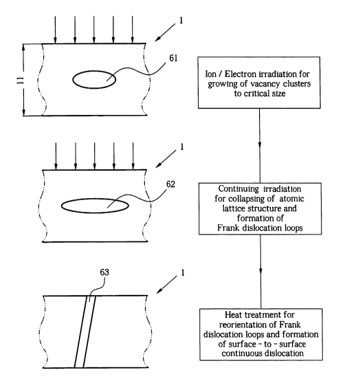
Fig. 3 illustrates the stages involved in the fabrication of
continuous dislocations. In a first stage, a thin film 1
previously fabricated with a predetermined thickness 11 is
exposed to ion irradiation or electron irradiation. The
thickness 11 is selected in conjunction with irradiation
parameters such that ions impinging at one surface may
8/15
CA 02487859 2004-11-29
WO 2004/040670 PCT/US2003/017432
propagate and dissipate across the thickness 11. For
example, a YSZ thin film may be fabricated with a thickness
of about 140nm. For details about fabrication of a
substantially fluid impermeable YSZ thin film it is referred
to the concurrently filed and cross-referenced application
titled "Sub-micron Electrolyte Thin Film on I~ano-Porous
Substrate by Oxidation of Metal Film".
The thickness 11 is selected for exemplary irradiation
parameters of 5x10¹⁵ ions/cm2 Xe3+ @ 450kV resulting in an
approximate dislocation density of 101 cm/cm3. During the
first stage, vacancy clusters 61 begin to form within the
crystalline structure of the thin film 1. As the irradiation
continues, the vacancy clusters 61 grow to a critical size.
Other ions such as Argon ions may be used besides Xenon ions.
The use of Xenon ions conforms to a well-known Transmission
Electron Microscope (TEM) observation. The use of Argon ions
to the contrary results in lower dislocation density but
deeper penetration, because Ar ion is smaller and lighter
than Xe. The use of electrons for irradiation provides much
deeper penetration because electron is much smaller than
ions. Penetration depth may estimated in a well-known
fashion such as with a commercially available software "SRIM-
2000.40" from IBM. For example, maximum penetration depth in
YSZ estimated for 450keV Ar ion irradiation may be about
340nm. Irradiation intensities are preferably kept to a
maximum for maximum penetration depth and higher dislocation
density. As may be well appreciated by anyone skilled in the
art, irradiation intensities are limited to levels at which
structural damage to the thin film 1 is substantially
avoided. In case, a thin film 1 may be accessed for
irradiation from both sides 12, 13, the maximum penetration
depth may be doubled.
9/15
CA 02487859 2004-11-29
WO 2004/040670 PCT/US2003/017432
At and beyond critical size and while irradiation continuous,
the surrounding atomic lattice structure collapses resulting
in a transformation of the vacancy clusters 61 into well-
known Frank dislocation loops 62. During that second stage,
the dipoles of the Frank dislocation loops 62 are at
arbitrary positions within the thin film 1. Ionic
conductivity may be improved by sole irradiation where Frank
dislocation loops are formed in arbitrary orientation.
Ionic conductivity may be brought to maximum levels for a
given dislocation density, where the Frank dislocation loops
are spatially reoriented such that both dipoles of the
dislocation loops coincide with top and bottom surfaces 12,
13 (see Fig. 5). In that way, continuous surface-to-surface
dislocations 63 are formed along which ions may propagate
between the surfaces 12, 13 with minimal activation energies.
The Frank dislocation loops are spatially reorientation after
completion of the irradiation during a separate heat
treatment of the thin film 1. For the case of an YSZ thin
film 1, the heat treatment may include an exposure to about
800°C for about 3 hr. The temperature is selected to
initiate growth and spatial reorientation of Frank
dislocation loops 62 without substantially reducing the
dislocation density due to undesired recombination of the
dislocation loops. At the end of the heat treatment, the
sample is gradually cooled off to prevent the formation of
cracks.
Fig. 4 shows an enlarged TEM photograph of a YSZ multilayer
cross section with a platinum layer 54 on top of a gold layer
53 on top of an irradiated YSZ layer 52 on top of a
substantially irradiation free YSZ bulk layer 51. The white
areas within layer 52 represent dislocations with a
dislocation density of about 1012 cm/cm3. The sample of Fig.
10/15
CA 02487859 2004-11-29
WO 2004/040670 PCT/US2003/017432
4 has gold and platinum layers 5 3, 54 on top of the
irradiated layer 52. Layers 53, 54 are deposited after
irradiation for sample preparation. Also for purposes of
sample preparation, the irradiated layer 52 has been
fabricated into a bulk layer of which an irradiation
unaffected portion 51 is visible in Fig. 4. The Frank
dislocation loops, visible as white areas within layer 52 are
not spatially reoriented. The sample of Fig. 4 is for the
sole purpose of observation.
Fig. 5 schematically illustrates the effect of continuous
surface-to-surface dislocations on ion propagation from one
thin film surface 13 to the opposite surface 12.
Besides YSZ, SDC is a preferred ceramic material for
electrolyte membranes. An SDC may have, for example the
chemical formula Smo,2Ceo,801.9 [20SDC] . Fig. 6 depicts
estimated conductivities as a function of temperature for
natural 8YS2 (curve 81) and 20SDC (curve 83) as well as 8YSZ
with dislocation densities of lOllcm/cm3 (curve 82) and
1014cm/cm3 (curve 84) and 20SDC with dislocation densities of
1011cm/cm3 (curve 85) and 1014cm/cm3 (curve 86) .
Fig. 7 shows a device 100 having a thin film 1 with
dislocations in accordance with the present invention. The
device 100 may be a fuel cell or a gas sensor.
It will be clear to a person of average skill in the art that
the above preferred embodiment may be altered in many ways
without departing from the scope of the invention. For
example, other fluorite materials, such as, but not limited
to, Ca stabilized zirconia and Sc stabilized zirconia may be
adopted as an electrolyte material. Also, well-known
Perovskite ion conducting materials may be adopted as an
electrolyte material.
11/15
CA 02487859 2004-11-29
WO 2004/040670 PCT/US2003/017432
Accordingly, the scope of the invention described in the
specification above is set forth by the following claims and
their legal equivalent:
12/15