Note: Descriptions are shown in the official language in which they were submitted.
CA 02510943 2005-06-28
- 1 -
METHOD AND APPARATUS FOR DETECTING OVERLAPPED SUBSTRATES
FIELD OF THE INVENTION
The present application is directed to a method
and apparatus for detecting overlapped substrates being
moved past an optical sensor. In particular, the method
and apparatus include a passage for transmitting single
substrates past an optical sensor designed to detect the
presence of overlapped substrates in such a series of
single substrates.
BACKGROUND OF THE INVENTION
In many document handling systems, documents such
as banknotes, cheques, cards, vouchers and the like, are
transported one by one along a transport path for
analysis and processing. The document handling system
includes sensors to identify information provided on the
document and to supply this information to a processing
means for determining how the document is to be
processed.
An undesirable situation may occur when two or
more documents are fed to the system at the same time.
This situation is known as a double feed document
condition and it is desirable to detect this condition
and reject or reprocess the documents to eliminate the
condition.
There are a number of known mechanical and
optical systems for detecting the double feed document
condition. One known mechanical technique effectively
uses mechanical means to contact the substrates and
determine a thickness or change in thickness thereof.
Examples of these techniques are shown in United States
Patents 3,679,202; United States Patent 4,550,252 and
United States Patent 5,704,246. Basically, the thickness
...,,.
CA 02510943 2005-06-28
- 2 -
of the documents in double feed document condition is
greater than some predetermined standard and an alarm or
stop signal is produced. This known technique is
difficult to use for thin documents and/or for documents
having a variable thickness as is often the case with
used banknotes. For example, with used banknotes the
banknotes May be creased or laminated with scotch tape
for example, making the thickness determination more
difficult. Furthermore, with these type of mechanical
thickness based structures it is difficult to maintain
the sensitivity of the measurement arrangement due to
vibration, wear, dirt variation in banknote condition and
other factors which will occur during prolonged use of
the device.
Optical double detection systems such as
disclosed in United States Patent 5,341,408; United
States Patent 5,502,312 and United States Patent
5,581,354 use at least one light emitter and a
corresponding light detector positioned on the opposite
side of the passage through which the documents are
transported. The light emitter generates a beam of light
which passes through the document in the passageway and
the transmitted light is detected by the light detector.
The light detector produces an output signal which is a
function of the light absorption and light scattering of
the document between the light emitter and the light
detector. The output signal is calibrated by various
means to a normal condition against which the actual
received conditions are compared. V~lhen a double feed
document condition occurs the double thickness of the
document significantly reduces the received light and a
sudden decreases in the signal is used to determine a
double feed document condition.
These prior art double feed detection systems are
...~ ,. .
~.~ ,
CA 02510943 2005-06-28
- 3 -
sensitive to variations caused by different paper,
varying surface color patterns and creases and folds in
the substrate. Variation will also occur due to
deterioration of the circuitry, voltage variation over
time and substrate placement in the passageway. Due to
these variations the systems require ongoing adjustment
of the preset signals of the light emitter and the light
detector. Unfortunately, these systems have low dynamic
range. Basically the systems are measuring the amount of
light which is transmitted through the document or
substrate and the amount of light can significantly vary
due to black marks or logos provided on the document, the
number of folds or creases in the paper and/or the
position of the document within the passageway.
Furthermore, worn and dirty single documents may be more
opaque than a double condition of two new documents.
United States Patent 5,222,729 discloses a method
and apparatus for detecting superimposed sheets of paper.
This system utilizes cooperating upper and lower laser
emitter and photo receiver pairs that are positioned
above and below the sheet transport path. Voltages that
are representative of the positions of the upper and
lower surfaces of the sheet are compared to assigned
values. If the actual values significantly exceed the
assigned values, a superimposed sheet condition signal is
produced and appropriate corrective action can be taken.
This technique is complicated and requires substantial
processing. It is difficult to use it for crumpled and
blazed documents.
The simple detection of has been difficult to
achieve particularly in a device which can be quickly
calibrated without substantial and time consuming
operator involvement. Also it has been difficult to
.., , .
CA 02510943 2005-06-28
- 4 -
achieve a detection arrangement which is reliable and
accurately identifies double feed document conditions.
The present invention seeks to overcome a number of
these deficiencies.
SUN~IARY OF THE PRESENT INVENTION
A method of detecting the occurrence of
overlapped substrates in a succession of single
substrates being moved past an optical sensor comprises
exposing each substrate as it is moved past the optical
senor to culminated coherent light where a portion of the
light is transmitted through the substrate and received
by a photo detector which produces an output signal where
the output signal where the output signal has a low
frequency component proportional to an average
transmitted light through the substrate and a high
frequency speckle flicker component produced by the rough
surface and movement of the substrate past the optical
sensor. The method includes monitoring the high
frequency speckle flicker component for a sudden drop in
the level thereof reflective of the reduced high
frequency component created when overlapped substrates
move past the optical sensor.
According to an aspect of the invention the
method includes using the optical sensor to determine a
first adaptive threshold as a predetermined amount of the
average signal from the photo detector when no document
is present and using the first adaptive threshold as a
reference to determine a change in signal indicative of a
substrate being moved past the optical sensor.
In yet a further aspect of the invention the
method includes setting a second adaptive threshold as a
predetermined amount of the high frequency speckle
. . . , y.1
CA 02510943 2005-06-28
- 5 -
flicker component during transport of a single substrate
past the optical sensor.
In yet a further aspect of the invention the
method includes automatic changeover from the first
adaptive threshold to the second adaptive threshold for
each substrate as it is moved past the optical sensor.
In yet a further aspect of the invention the
method includes using a photo detector having a narrow
aperture to produce the output signal.
In yet a further aspect of the invention the
method includes amplifying the output signal prior to
monitoring the high frequency speckle flicker component.
BRIEF DESCRIPTION OF THE DRAWINGS
The above as well as other advantages and
features of the present invention will be described in
greater detail according to the preferred embodiments of
the present invention in which;
Figure 1 is a schematic view showing a substrate
being moved past the optical senor;
Figure 2 is a schematic view illustrating the
type of signal produced when two substrates are moved
past the optical sensor;
Figure 3 is a schematic view showing the optical
sensor either side of a substrate passageway;
Figure 4 shows a circuit diagram used in the
processing of the signals;
Figure 5 is a double graph showing the signals
CA 02510943 2005-06-28
- 6 -
produced when a single hundred dollar currency document
is moved past the optical sensor and the signal when a
double condition occurs with two hundred dollar banknotes
being moved past the optical sensor in an overlapped
condition; and
Figure 6 is a graph similar to Figure 5 showing a
single document and a double document with dark markings
being provided on the single document.
DETAINED DESCRIPTION ACCORDING TO THE PREFERRED
EMBODIMENTS OF THE PRESENT INVENTION IN WHICH:
The present invention recognizes that the high
frequency speckle component from an optical sensor is
greatly effected when two banknotes are placed between
the optical sensor. Basically, a laser or other light
source produces a collimated light exposing one side of a
banknote as it is moved past the optical sensor. A photo
detector is provided on the opposite side of the
passageway and receives light which is transmitted
through the document. The surface of the banknote or
other substrates are relatively rough and produce
constructive light interference and destructive light
interference. This would be true of the light reflected
from the banknote and it is also true of the light which
is transmitted through the banknote. Basically the rough
surface of the substrate produces this interference.
Speckle flicker is produced due to the constructive
interference and this constructive interference
effectively appears to move due to the movement of the
banknote. Analysis of the output signal received from
the photo detector produces a low frequency component due
to of the transmitted light as well as a high frequency
speckle flicker component produced by the constructive
interference with the surface of the banknote or other
document. When two substrates are present as illustrated
,...,..~ . , .m.~ r
CA 02510943 2005-06-28
_ 7 _
in Figure 1B the high frequency speckle flicker component
is essentially eliminated or greatly reduced. Thus
monitoring of the high frequency speckle flicker
component and noting a sudden drop therein is indicative
of a double substrate condition.
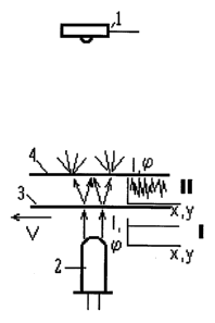
Figure 1A illustrates a speckle image
acquisition from single document, and figure 1B
illustrates a speckle image acquisition from doubled
document. In all illustrations the photo detector is
marked as 1, laser emitter as 2, single banknote as 3,
superimposed banknote as 4, V- speed of banknote
movement, f - laser beam diameter near banknote, z -
distance between banknote and photo detector, a - maximum
observation angle of illuminated spot on banknote. Insets
on Fig.l shows coordinate (x and y is the same)
dependence of illuminated beam intensity (I) and phase
(cp). Inset describes quasi-uniform laser beam
illuminated first banknote 3 surface. Inset ~~ describes
strongly non-uniform luminous flux after first banknote 3
which illuminates superimposed banknote 4. Under quasi-
uniform laser illumination the maximum speckle flicker
frequency F is about F=V~f /a,~z, where ~, is the laser
wavelength. Under typical values V=300mm/sec, f=l,2mm,
7~,=850nm, z=20mm the upper speckle flicker frequency is
F~20kHz and speckle flicker frequency band is in the
range of 1 to 20kHz. The superimposed banknote 4 is
illuminated by strongly non-uniform flux - speckle image
after first banknote 3 with typical spot size up to
hundreds times less than laser beam. As a result the
maximum speckle flicker frequency and light coherency
strongly decreases, so speckle signal from doubled
...~ »,
CA 02510943 2005-06-28
banknote falls dramatically (by a factor of 10 or
greater).
Figure 2 is a side view of an example of single
sensing assembly construction. The linear IC compact
photosensor 57815 from Hamamatsu is used as photodetector
1. VCSEL compact IR laser SV4637-001 from Honeywell is
used as emitter 2. Photo detector is mounted on PC board
6 with electronic components 5. Emitter 2 is mounted on
separate mini PC board 10 on the other side of passageway
formed by upper 7 and lower 8 walls with transparent
windows 9. Typical banknote transporting speed for
specified assembly is in the range 50 to 2000 mm/sec. In
order to increase the banknote speed a faster detector
with smaller sensing active area would be used.
Figure 3 shows a block diagram of hardware
components processing of speckle flicker signal in a
single sensing assembly. In order to take the calibration
signal from free channel and corresponding first adaptive
threshold, laser emitter 2 is constantly pumping from
generator 11 by pulses with duty factor 1/32. Photo
detector 1 at that time generates average signal (because
of photo detector vision persistence) proportional to
total transmission of free channel, windows 9 etc.
Typical the signal for the embodiment shown on Fig.2 lies
in the range 4 to 6 V. Upper frequency band alternating
component of said signal is amplified by upper-frequency
amplifier 14 and detected by linear detector 15. Typical
detector output signal under said conditions lies in the
range 2 to 3 V. A predetermined fraction (typically 1/5)
of the signal (generally set by resistors Rl, R2) is used
as first adaptive threshold. When the banknote enters the
",j"
,.., , .
CA 02510943 2005-06-28
- 9 -
sensing assembly (between laser and photo detector) photo
detector output average signal significantly falls
(commonly lowers 1.5 V) and comparator 13 with reference
Vrl switch on the key cell 12. The laser 2 is switched
into steady generation mode.
The banknote moving between the laser and the photo
detector causes the output signal of the photo detector
to have a steady component (proportional for average
banknote transmission) and alternating component
(proportional for speckle flicker). The upper frequency
band (speckle flicker component) of said alternating
component again is amplified by upper-frequency amplifier
14 and detected by linear detector 15. Typical the
detector output speckle flicker signal lies in the range
0,0.8 to 3 V depending on banknote type and condition. A
predetermined fraction (typically 1~) of the signal
(generally set by resistors R4, R5) is used as second
adaptive threshold.
Changeover time from first threshold to second
adaptive threshold is dependent on the characteristic
time of R4C4. When detector 15 output signal strongly
drops below the first or second threshold (it is typical
for doubled banknote) comparator 17 produces inhibiting
negative pulse. The delay circuit R6C5 and comparator 18
is used to inhibiting pulse time exceeding the transport
mechanism stop and/or crash-back time. In order to
eliminate error signals from banknote with wide opaque
places (like blazed hologram on EURO and new 100CD) the
increase of detector 15 integration time is provided by
connection additional capacity C3 with key cell 16.
. . .,., ,
CA 02510943 2005-06-28
- 10 -
Figure 4 shows a typical signals under steady laser
illumination of double banknote with blazed hologram
100CD which are shifted with space displacement about 50
mm. Scale factor for abscissa axis is 40 msec/point and
0.5 V/point for ordinate axis. So up to 25 msec from
beginning signals corresponds for free channel, from 25
msec to 160 msec - for single banknote, from 160 msec to
the end - for double banknote. In order to produce a more
pure consistent speckle flicker the signal laser emitter
produces a steady emission. Banknote movement speed is
about 300 mm/sec. The speckle signal is reflective of the
time dependence of detected speckle flicker signal with
banknote movement. The transmission signal describes the
time dependence of average banknote transmission at the
same point.
Figure 5 shows a typical signal under steady laser
illumination of a double banknote condition where the
banknotes include a plastic substrate and a dark surface
pattern 5 or Australian Dollars. The scale factor is the
same as in Fig.4. So up to 50 msec from beginning signals
corresponds for free channel, from 50 msec to 200 msec -
for single banknote, from 200 msec to the end - for
double banknote. In order to produce a more consistent
speckle flicker signal the laser emitter produces steady
emission. Banknote movement speed is about 300 mm/sec.
The speckle signal describes the time dependence of
detected speckle flicker signal with banknote movement.
The transmission signal describes the time dependence of
average banknote transmission at the same point.
The present invention is described herein in
the context of a double banknote checking application as
for bill feeder, bill dispenser or other bills handling
".i,.
CA 02510943 2005-06-28
- 11 -
device, in a bank, postal facility, supermarket, casino
or transportation facility. However, it is appreciated
that the embodiment shown and described herein may also
be useful for checking other doubled substrates,
particularly flat, substrates such as cards, films, paper
sheets and paintings. The checking device may be
stationary or portable, battery powered or powered by
connection to an electric outlet.
This arrangement is particularly suitable for
banknote validators that include an inlet for receiving a
stack of banknotes.
It is appreciated that various features of the
invention, which are, for clarity, described in the
context of single embodiment, may also be provided in
combination in series or another embodiments. Conversely,
various features of the invention which are, for brevity,
described in the context of a single embodiment, may also
be provided separately or in any suitable combination.
Although various preferred embodiments of the
present invention have been described in detail, it will
be appreciated by those skilled in the art that
variations may be made without departing from the spirit
of the invention or the scope of the appended claims.
._.. ~, ,..y,