Note: Descriptions are shown in the official language in which they were submitted.
CA 02517048 2005-08-25
Internal reference: IRDM.035 NON-EP / IDC-40001
CONDUCTIVE BUS STRUCTURE FOR INTERFEROMETRIC MODULATOR ARRAY
Background
Field of the Invention
The field of the invention relates to microelectromechanical systems (MEMS),
and more
particularly, to electrical connection architectures for arrays of MEMS
elements.
Description of the Related Technolo~y
Microelectromechanical systems (MEMS) include micromechanical elements,
actuators,
and electronics. Micromechanical elements may be created using deposition,
etching, and or
other micromachining processes that etch away parts of substrates and/or
deposited material
layers or that add layers to form electrical and electromechanical devices.
One type of MEMS
device is called an interferometric modulator. An interferometric modulator
may comprise a pair
of conductive plates, one or both of which may be partially transparent and
capable of relative
motion upon application of an appropriate electrical signal. One plate may
comprise a stationary
layer deposited on a substrate, the other plate may comprise a metallic
membrane suspended over
the stationary layer.
Arrays of independently actuatable interferometric light modulators are used
in certain
display configurations as display elements. The light modulators are
electrically connected so as
to provide the control voltages or signals used to individually actuate each
light modulator.
Summary of Certain Embodiments
The system, method, and devices of the invention each have several aspects, no
single
one of which is solely responsible for its desirable attributes. Without
limiting the scope of this
invention, its more prominent features will now be discussed briefly. After
considering this
discussion, and particularly after reading the section entitled "Detailed
Description of Certain
Embodiments" one will understand how the features of this invention provide
advantages over
other display devices.
In certain embodiments, a light modulator comprises a substrate, a first
electrode layer
over the substrate, and a second electrode layer over the substrate. The light
modulator further
comprises a reflective surface substantially parallel to the first electrode
layer and coupled to the
second electrode layer. The reflective surface is movable along a direction
substantially
perpendicular to the reflective surface between a first position and a second
position. The first
position is a first distance from the first electrode layer and the second
position is a second
distance from the first electrode layer. The light modulator further comprises
a conductive bus
-1-
CA 02517048 2005-08-25
layer of which at least a portion is electrically coupled to at least one of
the first electrode layer
and the second electrode layer. The reflective surface moves between the first
position and the
second position in response to a voltage applied to the conductive bus layer.
In certain embodiments, a method controls a light modulator. The method
comprises
providing a substrate and providing a first electrode layer over the
substrate. The method further
comprises providing a second electrode layer over the substrate and providing
a reflective surface
that is substantially parallel to the first electrode layer and coupled to the
second electrode layer.
The reflective surface is movable along a direction substantially
perpendicular to the reflective
surface between a first position and a second position. The first position is
a first distance from
the first electrode layer and the second position is a second distance from
the first electrode layer.
The method further comprises applying a voltage to a conductive bus layer,
wherein at least a
portion of the conductive bus layer is electrically coupled to at least one of
the first electrode
layer and the second electrode layer. The method further comprises moving the
reflective surface
between the first position and the second position in response to the applied
voltage.
In certain embodiments, a device comprises means for supporting an
interferometric
modulator. The device further comprises means for conducting a first
electrical signal over the
supporting means. The device further comprises means for conducting a second
electrical signal
over the supporting means. The device further comprises means for reflecting
light being
substantially parallel to the means for conducting the first electrical signal
and being coupled to
the means for conducting the second electrical signal, the means for
reflecting light being
movable along a direction substantially perpendicular to the means for
reflecting light and
movable between a first position and a second position, the first position
being a first distance
from the means for conducting the first electrical signal, the second position
being a second
distance from the means for conducting the first electrical signal. The device
further comprises
means for electrically coupling to at least one of the means for conducting
the first electrical
signal and the means for conducting the second electrical signal, wherein the
means for reflecting
light moves between the first position and the second position in response to
a voltage applied to
the means for electrically coupling.
Brief Description of the Drawings
Figure 1 is an isometric view depicting a portion of one embodiment of an
interferometric modulator display in which a movable reflective layer of a
first interferometric
modulator is in a released position and a movable reflective layer of a second
interferometric
modulator is in an actuated position.
Figure 2 is a system block diagram illustrating one embodiment of an
electronic device
incorporating a 3x3 interferometric modulator display.
-2-
CA 02517048 2005-08-25
Figure 3 is a diagram of movable mirror position versus applied voltage for
one
exemplary embodiment of an interferometric modulator of Figure 1.
Figure 4 is an illustration of a set of row and column voltages that may be
used to drive
an interferometric modulator display.
Figures SA and SB illustrate one exemplary timing diagram for row and column
signals
that may be used to write a frame of display data to the 3x3 interferometric
modulator display of
Figure 3.
Figure 6A is a cross section of the device of Figure 1.
Figure 6B is a cross section of an alternative embodiment of an
interferometric
modulator.
Figure 6C is a cross section of another alternative embodiment of an
interferometric
modulator.
Figure 7A schematically illustrates an exemplary 3x3 interferometric modulator
display
having a conductive bus located above the second electrode layer and
electrically coupled to the
first electrode layer.
Figure 7B shows a cross-sectional view of the 3x3 interferometric modulator
display of
Figure 7A.
Figure 7C is a view of a single post support from the 3x3 interferometric
modulator
display of Figure 7A with the conductive bus to second electrode layer
connection shown in
circular dashed lines.
Figure 8A schematically illustrates an exemplary 3x3 interferometric modulator
display
having a conductive bus located above the second electrode layer and
electrically coupled to the
second electrode layer.
Figure 8B shows a cross-sectional view of the 3x3 interferometric modulator
display of
Figure 8B.
Figure 9A schematically illustrates an exemplary 3x3 interferometric modulator
display
having a conductive bus located between the second electrode layer and the
first electrode layer
and electrically coupled to the first electrode layer.
Figure 9B shows a cross-sectional view of the 3x3 interferometric modulator
display of
Figure 9A.
Figure 9C schematically illustrates an exemplary 3x3 interferometric modulator
display
having a conductive bus located on and electrically coupled to the first
electrode layer.
Figure 9D shows a cross-sectional view of the 3x3 interferometric modulator
display of
Figure 9C.
Figure 9E shows a cross-sectional view of another embodiment of the 3x3
interferometric
modulator display of Figure 9C having a mask material aligned with the
conductive bus and
-3-
CA 02517048 2005-08-25
located between the conductive bus and the viewing side of the 3x3
interferometric modulator
display.
Figure 10A schematically illustrates an exemplary 3x3 interferometric
modulator display
having a first conductive bus located above the second electrode layer and
electrically coupled to
the first electrode layer and a second conductive bus located above the first
conductive bus and
electrically coupled to the second electrode layer.
Figure l OB shows a cross-sectional view of the 3x3 interferometric modulator
display of
Figure 10A.
Figures 11(A)-11(Q) schematically illustrate an exemplary series of processing
steps for
forming a conductive bus structure above the second electrode layer.
Figure 12 shows a cross-sectional view of an embodiment of an interferometric
modulator having an additional dielectric layer located within the optical
stack layer.
Figure 13 shows a cross-sectional view of an embodiment of an interferometric
modulator having air pockets located within the dielectric layer.
Figure 14 shows an embodiment of a patterned electrode with a decreased
electrically
active area.
Figure 15 is a cross-sectional view of an interferometric modulator
corresponding to
Figure 14 in a plane through active and inactive areas.
Figure 16 is another cross-sectional view of an interferometric modulator
corresponding
to Figure 14 in a plane through the active area only.
Figure 17 shows an alternative embodiment of a patterned electrode.
Figure 18 is a cross-sectional view of the interferometric modulator
corresponding to
Figure 17.
Figure 19 shows an embodiment of an interferometric modulator having the area
responsible for the electrostatic force decoupled from the reflective surface
layer.
Figure 20 shows an embodiment of the interferometric modulator of Figure 19 in
an
"On" state.
Figure 21 shows a perspective view of an embodiment of an interferometric
modulator
having a spring design for the second electrode layer.
Figure 22 shows a layout view of a pixel comprising a 3 x 3 array of
interferometric
modulators.
Figure 23 shows a cross-sectional view of an embodiment of a red
interferometric
modulator from the array in Figure 22.
Figure 24 shows a cross-sectional view of an embodiment of a green
interferometric
modulator from the array in Figure 22.
CA 02517048 2005-08-25
Figure 25 shows a cross-sectional view of an embodiment of a blue
interferometric
modulator from the array in Figure 22.
Figures 26A and 26B are system block diagrams illustrating an embodiment of a
visual
display device comprising a plurality of interferometric modulators.
Detailed Description of Certain Embodiments
An exemplary embodiment of an interferometric light modulator comprises a
substrate, a
first electrode layer over the substrate, a second electrode layer over the
substrate, and a
conductive bus layer. At least a portion of the conductive bus layer is
electrically coupled to at
least one of the first electrode layer and the second electrode layer. The
reflective surface moves
between the first position and the second position in response to a voltage
applied to the
conductive bus layer. The conductive bus layer provides an electrical path
that has significantly
lower electrical resistance than configurations which electrically connect
columns of
interferometric modulators only through the first electrode layer or connect
rows of
interferometric modulators only through the second electrode layer.
The following detailed description is directed to certain specific embodiments
of the
invention. However, the invention can be embodied in a multitude of different
ways. In this
description, reference is made to the drawings wherein like parts are
designated with like
numerals throughout. As will be apparent from the following description, the
invention may be
implemented in any device that is configured to display an image, whether in
motion (e.g., video)
or stationary (e.g., still image), and whether textual or pictorial. More
particularly, it is
contemplated that the invention may be implemented in or associated with a
variety of electronic
devices such as, but not limited to, mobile telephones, wireless devices,
personal data assistants
(PDAs), hand-held or portable computers, GPS receivers/navigators, cameras,
MP3 players,
camcorders, game consoles, wrist watches, clocks, calculators, television
monitors, flat panel
displays, computer monitors, auto displays (e.g., odometer display, etc.),
cockpit controls and/or
displays, display of camera views (e.g., display of a rear view camera in a
vehicle), electronic
photographs, electronic billboards or signs, projectors, architectural
structures, packaging, and
aesthetic structures (e.g., display of images on a piece of jewelry). MEMS
devices of similar
structure to those described herein can also be used in non-display
applications such as in
electronic switching devices.
One interferometric modulator display embodiment comprising an interferometric
MEMS display element is illustrated in Figure 1. In these devices, the pixels
are in either a
bright or dark state. In the bright ("on" or "open") state, the display
element reflects a large
portion of incident visible light to a user. When in the dark ("off ' or
"closed") state, the display
element reflects little incident visible light to the user. Depending on the
embodiment, the light
-5-
CA 02517048 2005-08-25
reflectance properties of the "on" and "off ' states may be reversed. MEMS
pixels can be
configured to reflect predominantly at selected colors, allowing for a color
display in addition to
black and white.
Figure 1 is an isometric view depicting two adjacent pixels in a series of
pixels of a
visual display, wherein each pixel comprises a MEMS interferometric modulator.
In some
embodiments, an interferometric modulator display comprises a row/column array
of these
interferometric modulators. Each interferometric modulator includes a pair of
reflective layers
positioned at a variable and controllable distance from each other to form a
resonant optical
cavity with at least one variable dimension. In one embodiment, one of the
reflective layers may
be moved between two positions. In the first position, referred to herein as
the released state, the
movable layer is positioned at a relatively large distance from a fixed
partially reflective layer. In
the second position, the movable layer is positioned more closely adjacent to
the partially
reflective layer. Incident light that reflects from the two layers interferes
constructively or
destructively depending on the position of the movable reflective layer,
producing either an
overall reflective or non-reflective state for each pixel.
The depicted portion of the pixel array in Figure 1 includes two adjacent
interferometric
modulators 12a and 12b. In the interferometric modulator 12a on the left, a
movable and highly
reflective layer 14a is illustrated in a released position at a predetermined
distance from a fixed
partially reflective layer 16a. In the interferometric modulator 12b on the
right, the movable
highly reflective layer 14b is illustrated in an actuated position adjacent to
the fixed partially
reflective layer 16b.
The fixed layers 16a, 16b are electrically conductive, partially transparent
and partially
reflective, and may be fabricated, for example, by depositing one or more
layers each of
chromium and indium-tin-oxide onto a transparent substrate 20. The layers are
patterned into
parallel strips, and may form row electrodes in a display device as described
further below. The
movable layers 14a, 14b may be formed as a series of parallel strips of a
deposited metal layer or
layers (orthogonal to the row electrodes 16a, 16b) deposited on top of posts
18 and an intervening
sacrificial material deposited between the posts 18. When the sacrificial
material is etched away,
the deformable metal layers are separated from the fixed metal layers by a
defined air gap 19. A
highly conductive and reflective material such as aluminum may be used for the
deformable
layers, and these strips may form column electrodes in a display device.
With no applied voltage, the cavity 19 remains between the layers 14a, 16a and
the
deformable layer is in a mechanically relaxed state as illustrated by the
pixel 12a in Figure 1.
However, when a potential difference is applied to a selected row and column,
the capacitor
formed at the intersection of the row and column electrodes at the
corresponding pixel becomes
charged, and electrostatic forces pull the electrodes together. If the voltage
is high enough, the
-6-
CA 02517048 2005-08-25
movable layer is deformed and is forced against the fixed layer (a dielectric
material which is not
illustrated in this Figure may be deposited on the fixed layer to prevent
shorting and control the
separation distance) as illustrated by the pixel 12b on the right in Figure 1.
The behavior is the
same regardless of the polarity of the applied potential difference. In this
way, row/column
actuation that can control the reflective vs. non-reflective pixel states is
analogous in many ways
to that used in conventional LCD and other display technologies.
Figures 2 through 5 illustrate one exemplary process and system for using an
array of
interferometric modulators in a display application. Figure 2 is a system
block diagram
illustrating one embodiment of an electronic device that may incorporate
aspects of the invention.
In the exemplary embodiment, the electronic device includes a processor 21
which may be any
general purpose single- or multi-chip microprocessor such as an ARM, Pentium ,
Pentium II~,
Pentium III'', Pentium IV~, Pentium Pro, an 8051, a MIPS~, a Power PC~, an
ALPHA~, or any
special purpose microprocessor such as a digital signal processor,
microcontroller, or a
programmable gate array. As is conventional in the art, the processor 21 may
be configured to
execute one or more software modules. In addition to executing an operating
system, the
processor may be configured to execute one or more software applications,
including a web
browser, a telephone application, an email program, or any other software
application.
In one embodiment, the processor 21 is also configured to communicate with an
array
controller 22. In one embodiment, the array controller 22 includes a row
driver circuit 24 and a
column driver circuit 26 that provide signals to a pixel array 30. The cross
section of the array
illustrated in Figure 1 is shown by the lines 1-1 in Figure 2. For MEMS
interferometric
modulators, the row/column actuation protocol may take advantage of a
hysteresis property of
these devices illustrated in Figure 3. It may require, for example, a 10 volt
potential difference to
cause a movable layer to deform from the released state to the actuated state.
However, when the
voltage is reduced from that value, the movable layer maintains its state as
the voltage drops back
below 10 volts. In the exemplary embodiment of Figure 3, the movable layer
does not release
completely until the voltage drops below 2 volts. There is thus a range of
voltage, about 3 to 7 V
in the example illustrated in Figure 3, where there exists a window of applied
voltage within
which the device is stable in either the released or actuated state. This is
referred to herein as the
"hysteresis window" or "stability window." For a display array having the
hysteresis
characteristics of Figure 3, the row/column actuation protocol can be designed
such that during
row strobing, pixels in the strobed row that are to be actuated are exposed to
a voltage difference
of about 10 volts, and pixels that are to be released are exposed to a voltage
difference of close to
zero volts. After the strobe, the pixels are exposed to a steady state voltage
difference of about 5
volts such that they remain in whatever state the row strobe put them in.
After being written,
each pixel sees a potential difference within the "stability window" of 3-7
volts in this example.
CA 02517048 2005-08-25
This feature makes the pixel design illustrated in Figure 1 stable under the
same applied voltage
conditions in either an actuated or released pre-existing state. Since each
pixel of the
interferometric modulator, whether in the actuated or released state, is
essentially a capacitor
formed by the fixed and moving reflective layers, this stable state can be
held at a voltage within
the hysteresis window with almost no power dissipation. Essentially no current
flows into the
pixel if the applied potential is fixed.
In typical applications, a display frame may be created by asserting the set
of column
electrodes in accordance with the desired set of actuated pixels in the first
row. A row pulse is
then applied to the row 1 electrode, actuating the pixels corresponding to the
asserted column
lines. The asserted set of column electrodes is then changed to correspond to
the desired set of
actuated pixels in the second row. A pulse is then applied to the row 2
electrode, actuating the
appropriate pixels in row 2 in accordance with the asserted column electrodes.
The row 1 pixels
are unaffected by the row 2 pulse, and remain in the state they were set to
during the row 1 pulse.
This may be repeated for the entire series of rows in a sequential fashion to
produce the frame.
Generally, the frames are refreshed and/or updated with new display data by
continually
repeating this process at some desired number of frames per second. A wide
variety of protocols
for driving row and column electrodes of pixel arrays to produce display
frames are also well
known and may be used in conjunction with the present invention.
Figures 4 and 5 illustrate one possible actuation protocol for creating a
display frame on
the 3x3 array of Figure 2. Figure 4 illustrates a possible set of column and
row voltage levels that
may be used for pixels exhibiting the hysteresis curves of Figure 3. In the
Figure 4 embodiment,
actuating a pixel involves setting the appropriate column to -Vb;as, and the
appropriate row to
+~V, which may correspond to -5 volts and +5 volts respectively Releasing the
pixel is
accomplished by setting the appropriate column to +Vb;as, and the appropriate
row to the same
+0V, producing a zero volt potential difference across the pixel. In those
rows where the row
voltage is held at zero volts, the pixels are stable in whatever state they
were originally in,
regardless of whether the column is at +Vb;as, or -Vb;as~
Figure SB is a timing diagram showing a series of row and column signals
applied to the
3x3 array of Figure 2 which will result in the display arrangement illustrated
in Figure SA, where
actuated pixels are non-reflective. Prior to writing the frame illustrated in
Figure SA, the pixels
can be in any state, and in this example, all the rows are at 0 volts, and all
the columns are at +S
volts. With these applied voltages, all pixels are stable in their existing
actuated or released
states.
In the Figure SA frame, pixels (1,1), (1,2), (2,2), (3,2) and (3,3) are
actuated. To
accomplish this, during a "line time" for row 1, columns 1 and 2 are set to -S
volts, and column 3
is set to +5 volts. This does not change the state of any pixels, because all
the pixels remain in
_g-
CA 02517048 2005-08-25
the 3-7 volt stability window. Row 1 is then strobed with a pulse that goes
from 0, up to 5 volts,
and back to zero. This actuates the (1,1) and (1,2) pixels and releases the
(1,3) pixel. No other
pixels in the array are affected. To set row 2 as desired, column 2 is set to -
5 volts, and columns
1 and 3 are set to +5 volts. The same strobe applied to row 2 will then
actuate pixel (2,2) and
release pixels (2,1) and (2,3). Again, no other pixels of the array are
affected. Row 3 is similarly
set by setting columns 2 and 3 to -5 volts, and column 1 to +5 volts. The row
3 strobe sets the
row 3 pixels as shown in Figure SA. After writing the frame, the row
potentials are zero, and the
column potentials can remain at either +5 or -5 volts, and the display is then
stable in the
arrangement of Figure SA. It will be appreciated that the same procedure can
be employed for
arrays of dozens or hundreds of rows and columns. It will also be appreciated
that the timing,
sequence, and levels of voltages used to perform row and column actuation can
be varied widely
within the general principles outlined above, and the above example is
exemplary only, and any
actuation voltage method can be used with the present invention.
The details of the structure of interferometric modulators that operate in
accordance with
the principles set forth above may vary widely. For example, Figures 6A-6C
illustrate three
different embodiments of the moving mirror structure. Figure 6A is a cross
section of the
embodiment of Figure l, where a strip of metal material 14 is deposited on
orthogonally
extending supports 18. In Figure 6B, the moveable reflective material 14 is
attached to supports
at the corners only, on tethers 32. In Figure 6C, the moveable reflective
material 14 is suspended
from a deformable layer 34. This embodiment has benefits because the
structural design and
materials used for the reflective material 14 can be optimized with respect to
the optical
properties, and the structural design and materials used for the deformable
layer 34 can be
optimized with respect to desired mechanical properties. The production of
various types of
interferometric devices is described in a variety of published documents,
including, for example,
U.S. Published Application 2004/0051929. A wide variety of well known
techniques may be
used to produce the above described structures involving a series of material
deposition,
patterning, and etching steps.
The response time for discharging and charging an interferometric modulator is
dependent in part on an RC (resistance-capacitance) time constant for the
voltage circuit
connected to the interferometric modulator. This response time of the
interferometric modulator
has an effect on the display quality of the interferometric modulator array.
When the time
between incoming scan pulses received by a given interferometric modulator is
shorter than the
response time of the interferometric modulator, the moving layer is unable to
synchronize with
the incoming scan pulses. Under such conditions, the state of the
interferometric modulator does
not respond to each and every scan pulse, thereby resulting in a degraded
displayed image. It is
-9-
CA 02517048 2005-08-25
therefore desirable to provide an interferometric modulator with a reduced
response time to allow
for faster scan and refresh rates.
The voltage circuit connected to an interferometric modulator comprises the
electrodes of
the interferometric modulator, as well as the contacts, conductors, and other
conductive elements
which provide electrical connections between the electrodes and the row/column
driver
electronics. In certain embodiments, the materials and geometries of the
electrodes of the
interferometic modulator impact the RC time constant for the voltage circuit.
In certain array
configurations, the electrodes of adjacent interferometric modulators are
coupled together in
series to connect adjacent interferometric modulators with the driver
electronics, resulting in
higher RC time constants. For other array configurations, wires or other
electrical connectors
may be utilized for the electrical connections between the row and column
drivers and the
electrodes of the interferometric modulators, with these wires contributing to
the RC time
constants of the interferometric modulators.
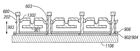
Figures 7A, 7B, and 7C schematically illustrate an exemplary 3x3 portion of an
interferometric modulator display in accordance with embodiments described
herein. Display
portions which are larger or smaller than the 3x3 portion illustrated in
Figure 7A are also
compatible with embodiments described herein. As shown in the cross-sectional
view of Figure
7B, each modulator comprises a substrate 1106, a first electrode layer 902
over the substrate
1106, and a second electrode layer 1302 over the substrate 1106. The modulator
further
comprises a reflective surface 901 which is substantially parallel to the
first electrode layer 902
and is coupled to the second electrode layer 1302. The reflective surface 901
is movable between
a first position and a second position. The first position of the reflective
surface 901 is a first
distance from the first electrode layer 902. The second position of the
reflective surface 901 is a
second distance from the first electrode layer 902.
In certain embodiments, as shown in Figure 7B, the first electrode layer 902
of each
modulator is fixed, and is positioned in proximity to the substrate 1106. The
first electrode layers
902 of the array are arranged in rows. These rows are not shown in Figure 7A,
but they
correspond to the three rows of modulators shown in Figure 7A. The first
electrode layers 902 of
each row are electrically connected to one another, but are electrically
insulated from the first
electrode layers 902 of the other rows.
In certain embodiments, the second electrode layer 1302 of each modulator
comprises at
least a portion of the moving layer above the first electrode layer 902. In
the embodiment
schematically illustrated by Figure 7A, the second electrode layer 1302
comprises the whole
moving layer. In certain embodiments, the second electrode layers 1302 of the
array are
patterned so as to separate the second electrode layers 1302 of each column of
modulators from
the second electrode layers 1302 of adjacent columns of modulators. Thus, the
second electrode
-10-
CA 02517048 2005-08-25
layers 1302 of the array are arranged in columns. For example, in the
embodiment schematically
illustrated by Figure 7A, the second electrode layers 1302 have straps or
tethers 1300 at the four
corners of the second electrode layer 1302 of each modulator. The tethers 1300
mechanically
couple the second electrode layers 1302 to the support posts 202 at the
corners of the modulators.
The tethers 1300 also electrically couple the second electrode layers 1302 of
adjacent modulators
within a column, while the second electrode layers 1302 are electrically
insulated from the
second electrode layers 1302 of the other columns. Other second electrode
layers 1302
compatible with embodiments described herein, have spring structures rather
than the tethers
1300 of Figure 7A.
In certain embodiments, as schematically illustrated by Figures 7A and 7B, the
reflective
surface 901 of each modulator is mechanically coupled to the second electrode
layer 1302 of the
corresponding modulator by a support member 1200. Certain other embodiments
comprise a
plurality of support members which mechanically couple the reflective surface
901 to the second
electrode layer 1302. Thus, when the modulator is activated, the reflective
surface 901 is moved
between the first position and the second position relative to the first
electrode layer 902 along a
direction 903 substantially perpendicular to the reflective surface 901.
In certain embodiments, each modulator of the array further comprises a
conductive bus
layer. At least a portion of the conductive bus layer is electrically coupled
to at least one of the
first electrode layer 902 and the second electrode layer 1302. The reflective
surface 901 moves
between the first position and the second position in response to a voltage
applied to the
conductive bus layer.
The conductive bus layer 600 of certain embodiments comprises a conductive
material,
including but not limited to, metals, composites, and alloys. Exemplary
conductive materials for
the conductive bus layer 600 include, but are not limited to, titanium,
chromium nickel, and
aluminum. In certain embodiments, the thickness of the conductive bus layer
600 is in a range
between approximately 0.1 micron and approximately 2 microns measured in a
direction that is
parallel to the direction 903 in Figure 7B. Other thicknesses are also
compatible with
embodiments described herein.
In certain embodiments, as shown in Figure 7A, the conductive bus layer 600 is
positioned above the second electrode layer 1302. The conductive bus layers
600 of the
modulators form a plurality of conductive bars, which in the exemplary
embodiment illustrated in
Figure 7A, are located above the second electrode layers 1302. The conductive
bars of each row
are electrically connected to one another and electrically insulated from the
conductive bars of
the other rows. In certain embodiments, each conductive bar provides
electrical connections
between a row driver and the first electrode layers 902 of a corresponding row
of modulators. In
certain embodiments, the width of the conductive bars running along the rows
is in a range
-11-
CA 02517048 2005-08-25
between approximately 4 microns and approximately 10 microns measured in a
direction that is
perpendicular to the direction 903 in Figure 7B. Other widths are also
compatible with
embodiments described herein.
In the exemplary embodiment illustrated in Figures 7A-7C, the conductive bus
layer 600
of a modulator is electrically coupled to the first electrode layer 902 of the
modulator by a
conductive portion of one or more of the support posts 202 of the modulator.
The support posts
202 provide structural support for the moving layer and the second electrode
layer 1302. In
certain embodiments, the conductive portions of the support posts 202 are
electrically coupled to
both the conductive bus layer 600 and the first electrode layer 902, but are
electrically insulated
from the second electrode layer 1302 by insulating material 603, as shown in
Figure 7B.
Figure 7C schematically illustrates a support post 202 of the 3x3 portion of
the
interferometric modulator display of Figure 7A compatible with embodiments
described herein.
The tethers 1300 are mechanically coupled to the support post 202, but are
electrically insulated
from the conductive bus layer 600 and from the electrically conductive portion
700 of the support
post 200. The electrically conductive portion 700 of the support post 200
electrically couples the
conductive bus layer 600 to the first electrode layer 902. As shown in Figure
7C, the electrically
conductive portion 700 of the support post 200 has a generally circular shape,
as illustrated by the
concentric dashed lines. In certain other embodiments, the conductive portion
700 has other
cross-sectional shapes (e.g., square). In certain embodiments, the conductive
portion 700 is
tubular, cylindrical, or solid. Embodiments of the conductive portion 700 may
have a uniform or
non-uniform cross-section between the conductive bus layers 600 and the first
electrode layers
902.
Advantageously, for the embodiments schematically illustrated by Figures 7A,
7B, and
7C, the conductive bus layer 600 is positioned over the second electrode layer
1302 and away
from the optical path of light entering or being reflected from the
interferometric modulator.
Thus, the conductive bus layer 600 of such embodiments does not interfere with
the optical
properties of the interferometric modulator. Furthermore, the conductive bus
layer 600
advantageously provides an electrical path between the row driver electronics
of the
interferometric modulator array and the first electrode layer 902 which has
significantly lower
electrical resistance than do other electrical paths of other configurations
(e.g., the first electrode
layers 902 of a row of interferometric modulators connected in series with one
another), thereby
advantageously reducing the RC time constant as compared to these other
configurations.
The conductive bus layer 600 of certain embodiments is positioned at various
locations
relative to the other portions of the display of interferometric modulators.
In certain
embodiments, as schematically illustrated by Figure 7A, the conductive bus
layer 600 is over the
second electrode layer 1302. As described below, in certain other embodiments,
the conductive
-12-
CA 02517048 2005-08-25
bus layer 600 is positioned within or adjacent to the first electrode layer
902, or between the first
electrode layer 902 and the second electrode layer 1302. The conductive bus
layer 600 can also
be located below the first electrode layer 902, or in substantially the same
plane as the second
electrode layer 1302. Other configurations of the conductive bus layer 600 are
also compatible
with embodiments described herein.
Figure 8A schematically illustrates an exemplary 3x3 portion of an
interferometric
modulator display having interferometric modulators in which the conductive
bus layer 800 is
located above the second electrode layer 1302 and is electrically coupled to
the second electrode
layer 1302. Figure 8B shows a cross-sectional view of the 3x3 portion of the
interferometric
modulator display of Figure 8A. In certain embodiments, as shown in Figure 8A,
the conductive
bus layers 800 of a column of modulators of the display are coupled together
to form a plurality
of conductive bars. The conductive bar of each column electrically connects
the second electrode
layers 1302 of the column to one another, and the conductive bar of each
column is electrically
insulated from the conductive bars of the other columns.
In certain embodiments, each conductive bar provides electrical connections
between a
column driver and the second electrode layers 1302 of the corresponding column
of modulators.
In certain embodiments, each conductive bus layer 800 is electrically
connected to the
corresponding second electrode layers 1302 at one or more locations. As
illustrated in Figure 8B,
the conductive bus layer 800 is connected to the second electrode layer 1302
over the support
posts 202. In certain embodiments, the width of the conductive bars running
along the columns is
in a range between approximately 4 microns and approximately 10 microns
measured in a
direction that is perpendicular to the direction 903 in Figure 8B. Other
widths are also
compatible with embodiments described herein. Advantageously, the conductive
bus layer 800
provides an electrical path between the column driver electronics of the
interferometric
modulator array which has significantly lower electrical resistance than do
other electrical paths
of other configurations (e.g., the second electrode layers 1302 of a column of
interferometric
modulators connected in series with one another), thereby advantageously
reducing the RC time
constant as compared to other configurations.
Figure 9A schematically illustrates an exemplary 3x3 portion of an
interferometric
modulator display having interferometric modulators in which the conductive
bus layer 900 is
located between the first electrode layer 902 and the second electrode layer
1302. Figure 9B
shows a cross-sectional view of the 3x3 portion of the interferometric
modulator display of
Figure 9A. In the exemplary embodiment illustrated in Figure 9A, the
conductive bus layer 900
is located below the second electrode layer 1302 and is a conductive portion
of the support posts
202 . In the embodiment schematically illustrated by Figure 9B, each
conductive bus layer 900 is
electrically coupled to each first electrode layer 902 of a row of
interferometric modulators and is
-13-
CA 02517048 2005-08-25
electrically isolated from the first electrode layers 902 of the other rows of
interferometric
modulators.
The conductive bus layer 900 of certain such embodiments electrically connects
a row
driver and the first electrode layers 902 of a corresponding row of
interferometric modulators.
The row driver selectively applies voltages through the conductive bus layer
900 to the first
electrode layers 902 of the interferometric modulators of a row of the
display. The conductive
bus layer 900 provides an electrical path that has significantly lower
electrical resistance than
configurations which electrically connect rows of interferometric modulators
only through the
first electrode layers 902.
Figure 9C schematically illustrates an exemplary 3x3 portion of an
interferometric
modulator display having interferometric modulators with a conductive bus
layer 1000 located
adjacent to and electrically coupled to the first electrode layers 902 of a
corresponding row of
interferometric modulators. Figure 9D shows a cross-sectional view of the 3x3
portion of the
interferometric modulator display of Figure 9C. The conductive bus layer 1000
of certain such
embodiments electrically connects a row driver and the first electrode layers
902 of a
corresponding row of interferometric modulators, thereby providing an
electrical path between
the row driver and the interferometric modulator that has significantly lower
electrical resistance
than other configurations which electrically connect rows of interferometric
modulators only
through the first electrode layers 902. In the exemplary embodiment
illustrated in Figure 9D, the
conductive bus layer 1000 is positioned between the support posts 202 and near
the periphery of
an underlying first electrode layer 902. The conductive bus layer 1000 is
electrically coupled to
the underlying first electrode layer 902.
The material for the conductive bus layer 1000 is selected to enhance the
conductivity
across the first electrode layers 902. In certain embodiments, the conductive
bus layer 1000
comprises aluminum or other conductive material. Unlike the first electrode
layers 902 of certain
embodiments, the material selected for the conductive bus layer 1000 may be
opaque. In certain
embodiments, the conductive bus layer 1000 has a width in a range between
approximately 4
microns and approximately 10 microns measured in a direction that is
perpendicular to the
direction 903 in Figure 9D.
In certain embodiments, a dielectric layer 906 is located between the
conductive bus
layer 1000 and the reflective surface layers 901. The dielectric layer 906 of
certain such
embodiments advantageously prevents contact between the conductive bus layer
1000 and the
reflective surface layer 901 of the interferometric modulator.
In certain embodiments, locating the conductive bus layer 1000 below the
reflective
surface layer 901 may adversely impact the optical performance of the
interferometric modulator
by blocking at least a portion of the incoming and reflected light of the
interferometric modulator.
-14-
CA 02517048 2005-08-25
To reduce the visual impact of the conductive bus layer 1000 on the optical
performance of the
interferometric modulator, conductive bus layers 1000 with smaller widths
measured in a
direction that is perpendicular to the direction 903 in Figure 9D can be
utilized.
Figure 9E shows a cross-sectional view of another embodiment of the 3x3
portion of the
interferometric modulator display of Figure 9C. The interferometric modulators
of the display
illustrated by Figure 9E have a mask material 1002 generally aligned with the
conductive bus
layers 1000 of the interferometric modulators and located between the
conductive bus layers
1000 and the viewing side of the 3x3 interferometric modulator display. The
mask material 1002
is a generally opaque and optically absorbing material with a sufficient width
to block incoming
light from impinging onto the conductive bus layers 1000. In the embodiment
illustrated in Figure
9E, the mask material 1002 is a generally coplanar in a layer 1004 with an
optically transmittive
material (e.g., Si02) which transmits incoming light to the modulators and
reflected light from the
modulators.
Figure 10A schematically illustrates an exemplary 3x3 portion of an
interferometric
modulator display having interferometric modulators with a first conductive
bus layer 1100
located over the second electrode layer 1302 and a second conductive bus layer
1102 located over
the first conductive bus layer 1100. Figure lOB shows a cross-sectional view
of the 3x3
interferometric modulator display of Figure 10A. The first conductive bus
layer 1100 is
electrically coupled through a conductive portion of at least one support post
202 to the first
electrode layers 902 of a row of interferometric modulators. The second
conductive bus layer
1102 is electrically coupled to the second electrode layers 1302 of a column
of interferometric
modulators. The first conductive bus layer 1100 is electrically isolated from
the second
conductive bus layer 1102 via insulating portions 605 of the support posts
202.
In Figure 10B, the first conductive bus layer 1100 is electrically coupled to
the first
electrode layer 902 through a conductive portion of one or more support posts
202. The second
conductive bus layer 1102 is electrically coupled to the second electrode
layer 1302 at locations
over one or more support posts 202.
In certain embodiments, the lower resistance path provided by the conductive
bus layers
advantageously reduces the RC time constant of the circuit. Exemplary RC times
for a plurality
of interferometric modulators having their first electrode layers 902
electrically coupled in series
can range from 5 microseconds to 100 microseconds, depending on the number of
interferometric
modulators. This same plurality of interferometric modulators may have a
resistance of as high
as 30-50 ohms/square. The use of the conductive bus layers to electrically
connect row and
column drivers to the corresponding first electrode layers 902 and second
electrode layers 1302
of the plurality of interferometric modulators can reduce the electrical
resistance of the circuit,
thereby reducing the RC time constant.
-15-
CA 02517048 2005-08-25
Method of Manufacture Conductive Bus over the Mechanical Laver
An exemplary series of processing steps for forming a conductive bus structure
located
above a second electrode layer 1302 is schematically illustrated in Figures
11(A)-11(Q). Figure
11 (A) shows the deposit of a black mask 1800 over a substrate 1106. In
certain embodiments, the
black mask 1800 comprises molybdenum.
Figure 11(B) shows the black mask 1800 patterned and etched to form islands on
top of
the substrate 1106. Figure 11 (C) shows the deposit of an oxide layer 1802
over the black mask
1800 and the substrate 1106, and the deposition of a metal layer 904 and a
first electrode layer
902 over the oxide layer 1802. In certain embodiments, the metal layer 904
comprises chromium
and the first electrode layer 902 comprises indium-tin-oxide (ITO).
Figure 11 (D) show the first electrode layer 902 and the metal layer 904 being
patterned
and etched to form electrodes and interferometric modulators compatible with
columns, rows, or
other useful configurations in accordance with the display design. In the
exemplary embodiment
illustrated in Figures 11(A)-11(Q), the first electrode layer 902 is usable as
a column electrode.
A dielectric (e.g., silicon oxide) layer 906 is formed over the metal layer
904, the first
electrode layer 902, and the oxide layer 1802, as illustrated in Figure 11(D).
Figure 11 (E) shows the formation of a sacrificial layer 1804. The sacrificial
layer 1804
determines the dimension of the cavity over which the reflective surface 901
is suspended. The
interference properties of the cavities are directly affected by their depth.
Certain embodiments
having color interferometric modulators construct modulators having cavities
of differing depths
which provide the resultant quiescent colors of red, green and blue. To
produce these varying
cavity dimensions, a different thickness of the sacrificial layer 1804 is
deposited for each of the
different colored interferometric modulators.
For example, in certain embodiments, a first sacrificial layer is deposited,
masked and
patterned, with the first sacrificial layer defining the area of a first
modulator. A second
sacrificial layer is then be deposited and patterned to define the combined
area of the first
modulator defined above and a second modulator. The combined thicknesses of
the first
sacrificial layer and the second sacrificial layer in the area of the first
interferometric modulator
is larger than the thickness of the second sacrificial layer in the area of
the second interferometric
modulator. Subsequently, in certain embodiments, a third sacrificial layer is
formed over the
second sacrificial layer defining the combined area of the first, second, and
third interferometric
modulator for each set of colored interferometric modulators. This third
sacrificial layer need not
be patterned in certain embodiments, since its thickness will be included in
all three of the
modulators of the set of colored interferometric modulators.
The three individual sacrificial layers described here may be of different
thicknesses. In
this way, the first modulator of the set of colored interferometric modulators
would have a cavity
-16-
CA 02517048 2005-08-25
depth equal to the combined thicknesses of the three sacrificial layers. The
second modulator of
the set of colored interferometric modulators would have a cavity depth equal
to the combined
thicknesses of two of the three sacrificial layers. The third modulator of the
set of colored
interferometric modulators would have a cavity depth equal to the thickness of
one of the three
sacrificial layers. When the sacrificial layers are removed, the cavity
dimensions will vary
according to the various combined thicknesses of the three sacrificial layers,
resulting in three
different colors such as red, green and blue.
Figure 11 (F) illustrates the deposition of a reflective surface layer 1901
over the
dielectric layer 906. In Figure 11 (G), the reflective surface layer 1901 was
patterned and etched
to form islands of the reflective surface layer 1901.
Figure 11 (H) illustrates the deposition of a sacrificial layer 1810 over the
reflective
surface layer 1901 and the dielectric layer 906. In certain embodiments, the
sacrificial layer 1810
comprises molybdenum.
In Figure 11 (I) the sacrificial layer 1810 has been patterned and etched to
form
conductive bus holes 1812 and reflective surface layer holes 1814. The
conductive bus holes
1812 extend through the sacrificial layer 1810 and intervening layers to the
first electrode layer
902. The reflective surface layer holes 1814 extend through the sacrificial
layer 1810 to the
reflective surface layer 1901.
In Figure 11(J), a conductive layer 1816 is deposited over the sacrificial
layer 1810 and
in the conductive bus holes 1812 and the reflective surface layer holes 1814.
The conductive
layer 1816 is electrically coupled to the first electrode layer 902 through
the conductive bus holes
1812. The conductive layer 1816 is also electrically coupled to the reflective
surface layer 1901
through the reflective surface layer holes 1814.
In Figure 11(K), the conductive layer 1816 is patterned and etched to form a
conductive
bus structure 1820 and reflective surface layer connectors 1818. The
reflective surface layer
connectors 1818 illustrated in Figure 11(K) are electrically isolated from the
conductive bus
structure 1820.
In Figure 11(L), a dielectric layer 1824 is deposited. In Figure 11(M), the
dielectric layer
1824 is patterned and etched to remove portions of the dielectric layer 1824
in regions located
between the conductive bus structure 1820 and the reflective surface layer
connectors 1818.
Figure 11 (N) illustrates the deposition of a sacrificial layer 1826. In
Figure 11 (O), the
sacrificial layer 1826 is patterned and etched to form landings 1828 for a
second electrode layer
1302. In Figure 11(P), the second electrode layer 1302 has been deposited,
patterned, and etched.
In Figure 11(Q), the sacrificial layers 1804, 1810, 1826 are removed,
resulting in the
interferometric modulator having the bus structure 1820.
-17-
CA 02517048 2005-08-25
Alone, or in combination with the features described above, the capacitance of
the
interferometric modulators can be reduced. Reducing the capacitance of the
circuit reduces the
RC time constant.
Refresh Rate
The time required to charge and discharge or change the applied voltage across
the first
electrode layer 902 and the second electrode layer 1302 affects the refresh
rate of the display.
For example, a decrease in the reaction time of the second electrode layer
1302 to changes in the
applied voltage allows the display to refresh in less time. A faster
refreshing display can provide
a less noticeable transition between subsequent frames.
Image Resolution
In certain embodiments, the use of a conductive bus structure comprising
complex
routing lines along the backside of an array of interferometric modulators
improves gray scale
display techniques. Techniques for displaying a gray scale image include the
subdividing of
pixels into a plurality of interferometric modules or smaller sub-pixels. By
having more sub-
pixels in each pixel, deeper grayscales can be achieved. However, increasing
the number of sub-
pixels increases the complexity of the required routing to the row and column
drivers located at
the perimeter of the display array.
In certain embodiments, the use of a conductive bus structure improves the
gray scale
display. In temporal modulation, each interferometric modulator of a grayscale
image is pulsed
or rapidly refreshed so that the viewer perceives the display to be exhibiting
variations in
intensity level. In certain embodiments, the refresh or modulation rate of the
interferometric
modulator is increased with the incorporation of one or more of the
modifications described
above. The refresh rate can be calculated by the following calculation:
T_line = T_rc + T_interferometric modulator
where T_line is the time to update 1 line;
T_rc is the RC time for the line;
T-interferometric modulator is the mechanical response time of the
interferometric
modulator.
Then:
T_refresh = n_rows x T_line
where T_refresh is the time it takes to update the entire screen;
n_rows is the number of rows on the display
Then:
Screen Refresh Rate = 1 / T refresh
where Screen Refresh Rate is the update rate of the entire display, typically
in Hz.
Thus, as T rc is decreased with the use of the conductive bus, T line
decreases and
T refresh decreases. As T refresh decreases, the Screen Refresh Rate increases
and enhances
temporal modulation.
-18-
CA 02517048 2005-08-25
Referring back to Figures 7A and 7B, the first electrode layer 902 has an
intrinsic
conductivity depending on the material selected for the first electrode layer
902. The electrical
circuit resistance of the interferometric modulator can be reduced by
utilizing a material for the
first electrode 902 that has a higher conductivity. In certain embodiments,
the material selected
for the first electrode layer 902 comprises zinc tin oxide (ZnTO) which has a
higher conductivity
as compared to indium tin oxide (ITO).
The thickness of the first electrode layer 902 may vary. In certain
embodiments, the
thickness may be between 300 angstroms and 2,000 angstroms measured in a
direction that is
parallel to the direction 903 in Figure 7B. Other thicknesses of the first
electrode layer 902 may
be used.
A material with a low dielectric constant can be selected for the oxide layer
or dielectric
material 906 that separates the first electrode layer 902 from the second
electrode layer 1302.
The dielectric electrically insulates the second electrode layer 1302 from the
first electrode layer
902 allowing a charge or voltage to be stored between the first and second
electrode layers. The
dielectric layer 906 further allows the voltage or charge to form an electro-
static force that acts
upon the second electrode layer 1302. A material having a low dielectric
constant
advantageously reduces the RC time constant of the electrical circuit. For
example, a low
dielectric constant (K) material can have a lower dielectric constant than a
dielectric made from
silicon dioxide (3.8). In certain embodiments, the dielectric constant of the
dielectric layer 906 is
as low as 2Ø
Reduce Capacitance
Different and additional materials can be added to reduce the capacitance of
the electrical
circuit. In certain embodiments, the material selected for the dielectric
layer 906 can reduce the
capacitance of the electrical circuit. These materials include spun-on-glass,
SiN, SiOz, A102, and
composites of one or more of these materials.
In certain embodiments, a second dielectric layer 104 is provided between the
metal layer
904 and the first electrode layer 902. In certain embodiments, as illustrated
in Figure 12, the
second dielectric layer 104 is located between the metal layer 904 and the
first electrode layer
902. This added dielectric layer 104 is in addition to the dielectric or oxide
layer 906. In such
embodiments, the dielectric layer 104 separates the optical functions of the
metal layer 904 from
the electrical functions of the first electrode layer 902. In certain
embodiments, this
configuration does not adversely impact the image quality of the display.
In certain embodiments of interferometric modulators, the reduction in
capacitance due to
the addition of the second dielectric layer 104 is a function of the
thicknesses of the dielectric
layer 906 and the second dielectric layer 104 when the reflective surface 901
is in the 'near'
position. In certain embodiments, the two dielectric layers 906, 104 comprise
the same material,
-19-
CA 02517048 2005-08-25
while in other embodiments, the two dielectric layers comprise different
materials. The
capacitance of an interferometric modulator can be approximated by the
equation below when the
dielectric layer 906 and the second dielectric layer 104 are the same
material.
Capacitance ~ (Area of the reflective surface 901) x (Dielectric Constant) x
(Permittivity
Constant) / (Thickness of Top Dielectric 906 + Thickness of Bottom Dielectric
104).
In certain embodiments, the thickness of the dielectric layer 906 may vary. As
illustrated
in Figure 13, the dielectric layer 906 comprises one or more air gaps 1900
embedded within the
dielectric layer 906.
Figures 14 and 17 illustrate an array of adjacent interferometric modulators
110 arranged
in rows and columns, each having a center portion of the first electrode layer
902 that is
electrically isolated from a peripheral portion of the first electrode layer
902. In certain
embodiments, cuts in the first electrode layer 902 separate the center portion
from the peripheral
portion. In certain such embodiments, the area of the portion of the first
electrode layer 902
participating in the driving of the interferometric modulator is reduced,
thereby reducing the
capacitance of the circuit.
In certain embodiments, only the peripheral portion contributes to the
electrically active
area of the first electrode layer 902. In certain such embodiments, the
peripheral portions are
electrically connected to a conductive bus structure. In certain other
embodiments, only the
center portion contributes to the electrically active area of the first
electrode layer 902. In certain
such embodiments, the center portions are electrically connected to a
conductive bus structure.
Figures 15 and 16 are cross-sections of two adjacent interferometric
modulators from Figure 14
having an electrically active center portion 902(a) which is electrically
isolated from a peripheral
portion 902(b) of both interferometric modulators.
Figure 17 illustrates an array of interferometric modulators 112 arranged in
rows and
columns, each interferometric modulator 112 having a first electrode layer 902
with a column
portion 902(c) that is electrically isolated from two peripheral portions
902(d), 902(e) of the first
electrode layer 902. In certain embodiments, one or more of the peripheral
portions 902(c),
902(d), 902(e) contribute to the electrically active area of the first
electrode layer 902 and one or
more of the peripheral portions 902(c), 902(d), 902(e) do not contribute to
the electrically active
area of the first electrode layer 902. Figure 18 is a cross-section view of
two interferometric
modulators 112 from Figure 17 having electrically active peripheral portions
902(d), 902(e)
electrically isolated from non-electrically active column portions 902(c) of
both interferometric
modulators.
Figures 19 and 20 illustrate an embodiment of an interferometric modulator
having a first
electrode layer 902 comprising more than two electrically active areas 404(a)-
(e). Together, the
electrically active areas 404(a)-(e) and the second electrode layer 1302 form
an electrostatic force
-20-
CA 02517048 2005-08-25
which pulls the second electrode layer 1302 towards the electrically active
areas 404(a)-(e). As
the second electrode layer 1302 moves towards the electrically active areas
404(a-(e), the
reflective surface 901 moves a corresponding distance relative to the
substrate 1106 and the metal
layer 904. The movement of the reflective surface 901 turns the
interferometric modulator 'ON'
S or 'OFF' as described above. By decoupling the two functions, the area of
the electrically active
portion of the optical layer (or of the mechanical layer) can be reduced to be
smaller than the area
of the optical portion of the optical layer (or of the mechanical layer).
Reduce Power Consumption
An additional benefit of reducing the resistance or capacitance of the circuit
is a
reduction in power consumption. For example, to charge and discharge an array
of
interferometric modulators, the column and row drivers require power to charge
and discharge
the interferometric modulators. By reducing the capacitance of the individual
interferometric
modulators, the row and column drivers can apply a lower voltage when
activating each
interferometric modulator. In certain embodiments, a reduction in the
activation voltage is
achieved by changing the mechanical stiffness of the interferometric module
and/or affecting the
strength of the electrostatic force within the interferometric modulator.
For example, geometric changes of the interferometric module can reduce the
mechanical
stiffness of the second electrode layer 1302. Exemplary geometric changes
include increasing
the spacing between adjacent support posts 202 or changing the shape of the
second electrode
layer 1302. In certain embodiments, increasing the nominal spacing between
support posts 202
increases the flexibility of the second electrode layer 1302 attached thereto.
This increase in
flexibility allows the second electrode layer 1302 and the reflective surface
901 to change states
in response to the column or row driver applying a lower activation voltage.
In certain embodiments, as shown in Figure 21, the geometry of the second
electrode
layer 1302 can be changed so as to simulate a mechanical spring. The
mechanical spring design
de-couples the reflective surface 901 from the second electrode layer 1302.
Tethers 120
constitute a spring portion while the reflective surface 901 moves up and
down. In certain
embodiments, the reflective surface 901 comprises a portion of a rigid body,
such as a reflective
surface layer. In this way, the tethers 120 and reflective surface 901 are
decoupled in that
movement of one does not substantially affect the other.
The selection of the material for the second electrode layer 1302 can affect
the activation
voltage. Selecting a more compliant material increases the flexibility of the
second electrode
layer 1302. In this way, in certain embodiments, the row and column drivers
apply a lower
activation voltage and still achieve the desired reflective surface layer
displacement. In certain
embodiments, the second electrode layer 1302 comprises a more compliant
material such as
aluminum to allow the reflective surface layer 901 to respond to a lower
activation voltage than
-21-
CA 02517048 2005-08-25
does a second electrode layer 1302 comprising nickel. Other exemplary
materials that could be
used for the second electrode layer 1302 include, but are not limited to, Cr,
Cu, composites made
of oxides and metal (for example, Silicon Nitride encased by aluminum),
organic films reinforced
by metal (for example, photoresist plated with any of the metal examples). The
mechanical
stiffness of the second electrode layer 1302 can be further decreased by
reducing the thickness of
the second electrode layer 1302. In certain embodiments, the second electrode
layer 1302 has a
thickness of about 500 angstroms.
Another technique in certain embodiments for reducing the activation voltage
is to
change the strength of the electric field created between the first electrode
layer 902 and the
second electrode layer 1302. The strength of the electric field is increased
by patterning the first
electrode layer 902 to reduce the amount of electrically active area. In this
way, the area of the
interferometric modulator which forms the electrically active portion is
reduced. Patterning the
electrode by decreasing the electrically active area as illustrated in Figures
14-18 has the effect of
increasing the actuation voltage assuming all other parameters are held
constant.
The activation voltage can be further reduced in certain embodiments by
selecting
materials for the one or more dielectric layers 906 that have higher
dielectric constants. To first
order, the relationship between dielectric constant and actuation voltage is:
V ~ 1/(K~1/2).
The voltage is inversely proportional to the square root of the dielectric
constant. Thus,
as the constant is increased, it takes less voltage to pull the second
electrode layer 1302 towards
the first electrode layer 902. Materials with higher dielectric constants
increase the resulting
electrostatic attraction between the first and second electrode layers.
One possible pixel configuration 602 in accordance with certain embodiments is
shown
in Figure 22. This view is as seen by the viewer from the front surface of a
substrate 106, and is
comprised of nine elements, three for each of the colors red, green and blue.
The modulators
1400(a), 1400(b), 1400(c) may correspond to red, 1400(d), 1400(e), 14000 to
green and
1400(g), 1400(h), 1400(i) to blue, as shown. The array of interferometric
modulators in the
embodiment schematically illustrated by Figure 22 is arranged in an N x N
matrix so as to
provide a display surface for an image.
The three different colors (red, green, and blue) may be achieved in certain
embodiments
by varying the distance between the mirror and the optical stack. When a
voltage is applied to the
modulators, they may all move a uniform distance towards the electrode or they
may all move
different distances toward the electrode. Indeed, all nine modulators may
traverse the entire
cavity and move to a near position that brings them into direct contact with
the substrate 106.
The dimensions of the cavities in the quiescent state are shown by the
vertical dimensions 1500,
1600 and 1700, in Figures 23, 24 and 25, respectively. In one embodiment, the
vertical
-22-
CA 02517048 2005-08-25
dimensions 1500, 1600, and 1700 are 4000 angstroms, 3000 angstroms, and 2000
angstroms,
respectively.
Interferometric modulators are minuscule, typically 25-60 microns on a side
(400-1,000
dots per inch). Therefore, in certain embodiments, many interferometric
modulators elements
can be ganged and driven together as a pixel, or sub-pixel in a monochrome,
color, or grayscale
display. For example, each interferometer modulator can correspond to a single
display pixel in a
monochrome display. For color or grayscale displays, the color or intensity of
each
interferometric modulator in certain embodiments is determined by the size of
the air gap
between the optical and mechanical layers. Multiple sub-elements having
different intensities or
colors form a grayscale or color pixel. To create a flat panel display, a
large array of
interferometric modulators are fabricated in the desired format (for example,
5" full color VGA)
and packaged.
The reflective surface 901 of modulator 1400(a) in certain embodiments may
have back
supports, a flex layer and support post interfaces designed to cause the
reflective surface 901 to
settle at a distance 1500. The reflective surface 901 of modulator 1400(d) in
certain
embodiments may have back supports, a flex layer, and support post interfaces
designed to cause
the reflective surface layer to settle at a distance 1600 that is less than
distance 1500. Finally, the
reflective surface layer 901 of modulator 1400(g) in certain embodiments may
have back
supports, a flex layer and support post interfaces designed to cause the
reflective surface layer to
settle at a distance 1700 that is less than the distance 1600. In this way,
controlling the
mechanical properties and/or the physical restraints of the supports in
certain embodiments
results in three different cavity dimensions, and thus three different pixel
colors are created.
Alternatively, the differing characteristics of the flex layer and supports
could be
manipulated to cause the reflective surface layer 901 to move different
distances upon application
of the same voltage. As yet another alterative, the modulators could all have
the same structures,
but differing voltages applied for differing colors.
Figures 26A and 26B are system block diagrams illustrating an embodiment of a
display
device 2040. The display device 2040 can be, for example, a cellular or mobile
telephone.
However, the same components of display device 2040 or slight variations
thereof are also
illustrative of various types of display devices such as televisions and
portable media players.
The display device 2040 includes a housing 2041, a display 2030, an antenna
2043, a
speaker 2045, an input device 2048, and a microphone 2046. The housing 2041 is
generally
formed from any of a variety of manufacturing processes as are well known to
those of skill in
the art, including injection molding, and vacuum forming. In addition, the
housing 2041 may be
made from any of a variety of materials, including but not limited to plastic,
metal, glass, rubber,
and ceramic, or a combination thereof. In one embodiment the housing 2041
includes removable
-23-
CA 02517048 2005-08-25
portions (not shown) that may be interchanged with other removable portions of
different color,
or containing different logos, pictures, or symbols.
The display 2030 of exemplary display device 2040 may be any of a variety of
displays,
including a bi-stable display, as described herein. In other embodiments, the
display 2030
includes a flat-panel display, such as plasma, EL, OLED, STN LCD, or TFT LCD
as described
above, or a non-flat-panel display, such as a CRT or other tube device, as is
well known to those
of skill in the art. However, for purposes of describing the present
embodiment, the display 2030
includes an interferometric modulator display, as described herein.
The components of one embodiment of exemplary display device 2040 are
schematically
illustrated in Figure 26B. The illustrated exemplary display device 2040
includes a housing 2041
and can include additional components at least partially enclosed therein. For
example, in one
embodiment, the exemplary display device 2040 includes a network interface
2027 that includes
an antenna 2043 which is coupled to a transceiver 2047. The transceiver 2047
is connected to the
processor 2021, which is connected to conditioning hardware 2052. The
conditioning hardware
2052 may be configured to condition a signal (e.g. filter a signal). The
conditioning hardware
2052 is connected to a speaker 2045 and a microphone 2046. The processor 2021
is also
connected to an input device 2048 and a driver controller 2029. The driver
controller 2029 is
coupled to a frame buffer 2028 and to the array driver 2022, which in turn is
coupled to a display
array 2030. A power supply 2050 provides power to all components as required
by the particular
exemplary display device 2040 design.
The network interface 2027 includes the antenna 2043 and the transceiver 2047
so that
the exemplary display device 2040 can communicate with one or more devices
over a network.
In one embodiment the network interface 2027 may also have some processing
capabilities to
relieve requirements of the processor 2021. The antenna 2043 is any antenna
known to those of
skill in the art for transmitting and receiving signals. In one embodiment,
the antenna transmits
and receives RF signals according to the IEEE 802.11 standard, including IEEE
802.11(a), (b), or
(g). In another embodiment, the antenna transmits and receives RF signals
according to the
BLUETOOTH standard. In the case of a cellular telephone, the antenna is
designed to receive
CDMA, GSM, AMPS or other known signals that are used to communicate within a
wireless cell
phone network. The transceiver 2047 pre-processes the signals received from
the antenna 2043
so that they may be received by and further manipulated by the processor 2021.
The transceiver
2047 also processes signals received from the processor 2021 so that they may
be transmitted
from the exemplary display device 2040 via the antenna 2043.
In an alternative embodiment, the transceiver 2047 can be replaced by a
receiver. In yet
another alternative embodiment, network interface 2027 can be replaced by an
image source,
which can store or generate image data to be sent to the processor 2021. For
example, the image
-24-
CA 02517048 2005-08-25
source can be a digital video disc (DVD) or a hard-disc drive that contains
image data, or a
software module that generates image data.
Processor 2021 generally controls the overall operation of the exemplary
display device
2040. The processor 2021 receives data, such as compressed image data from the
network
interface 2027 or an image source, and processes the data into raw image data
or into a format
that is readily processed into raw image data. The processor 2021 then sends
the processed data
to the driver controller 2029 or to frame buffer 2028 for storage. Raw data
typically refers to the
information that identifies the image characteristics at each location within
an image. For
example, such image characteristics can include color, saturation, and gray-
scale level.
In one embodiment, the processor 2021 includes a microcontroller, CPU, or
logic unit to
control operation of the exemplary display device 2040. Conditioning hardware
2052 generally
includes amplifiers and filters for transmitting signals to the speaker 2045,
and for receiving
signals from the microphone 2046. Conditioning hardware 2052 may be discrete
components
within the exemplary display device 2040, or may be incorporated within the
processor 2021 or
other components.
The driver controller 2029 takes the raw image data generated by the processor
2021
either directly from the processor 2021 or from the frame buffer 2028 and
reformats the raw
image data appropriately for high speed transmission to the array driver 2022.
Specifically, the
driver controller 2029 reformats the raw image data into a data flow having a
raster-like format,
such that it has a time order suitable for scanning across the display array
2030. Then the driver
controller 2029 sends the formatted information to the array driver 2022.
Although a driver
controller 2029, such as a LCD controller, is often associated with the system
processor 2021 as a
stand-alone Integrated Circuit (IC), such controllers may be implemented in
many ways. They
may be embedded in the processor 2021 as hardware, embedded in the processor
2021 as
software, or fully integrated in hardware with the array driver 2022.
Typically, the array driver 2022 receives the formatted information from the
driver
controller 2029 and reformats the video data into a parallel set of waveforms
that are applied
many times per second to the hundreds and sometimes thousands of leads coming
from the
display's x-y matrix of pixels.
In one embodiment, the driver controller 2029, array driver 2022, and display
array 2030
are appropriate for any of the types of displays described herein. For
example, in one
embodiment, driver controller 2029 is a conventional display controller or a
bi-stable display
controller (e.g., an interferometric modulator controller). In another
embodiment, array driver
2022 is a conventional driver or a bi-stable display driver (e.g., an
interferometric modulator
display). In one embodiment, a driver controller 2029 is integrated with the
array driver 2022.
Such an embodiment is common in highly integrated systems such as cellular
phones, watches,
-25-
CA 02517048 2005-08-25
and other small area displays. In yet another embodiment, display array 2030
is a typical display
array or a bi-stable display array (e.g., a display including an array of
interferometric
modulators).
The input device 2048 allows a user to control the operation of the exemplary
display
device 2040. In one embodiment, input device 2048 includes a keypad, such as a
QWERTY
keyboard or a telephone keypad, a button, a switch, a touch-sensitive screen,
a pressure- or heat-
sensitive membrane. In one embodiment, the microphone 2046 is an input device
for the
exemplary display device 2040. When the microphone 2046 is used to input data
to the device,
voice commands may be provided by a user for controlling operations of the
exemplary display
device 2040.
Power supply 2050 can include a variety of energy storage devices as are well
known in
the art. For example, in one embodiment, power supply 2050 is a rechargeable
battery, such as a
nickel-cadmium battery or a lithium ion battery. In another embodiment, power
supply 2050 is a
renewable energy source, a capacitor, or a solar cell, including a plastic
solar cell, and solar-cell
paint. In another embodiment, power supply 2050 is configured to receive power
from a wall
outlet.
In some implementations control programmability resides, as described above,
in a driver
controller which can be located in several places in the electronic display
system. In some cases
control programmability resides in the array driver 2022. Those of skill in
the art will recognize
that the above-described optimization may be implemented in any number of
hardware and/or
software components and in various configurations.
While the above detailed description has shown, described, and pointed out
novel
features of the invention as applied to various embodiments, it will be
understood that various
omissions, substitutions, and changes in the form and details of the device or
process illustrated
may be made by those skilled in the art without departing from the spirit of
the invention.
Methods for incorporating the features described above with the
interferometric modulators will
be readily apparent to one having ordinary skill in the art. Further, one or
more of these features
may be adapted to work with any of the embodiments, as well as other
configurations of the
interferometric modulators. As will be recognized, the present invention may
be embodied
within a form that does not provide all of the features and benefits set forth
herein, as some
features may be used or practiced separately from others.
-26-