Note: Descriptions are shown in the official language in which they were submitted.
CA 02520384 2005-09-20
Internal Reference: IROM.097 NON-EP / IOC-040052
PHOTONIC MEMS AND STRUCTURES
Background
This invention relates to microelectromechanical systems (MEMS).
Microelectromechanical systems (MEMS) include micromechanical elements,
actuators,
and electronics. Micromechanical elements may be created using deposition,
etching, and or
other micromachining processes that etch away parts of substrates and/or
deposited material
layers or that add layers to form electrical and electromechanical devices.
One type of MEMS
device is called an interferometric modulator. As used herein, the term
interferometric modulator
or interferometric light modulator refers to a device that selectively absorbs
and/or reflects light
using the principles of optical interference. In certain embodiments, an
interferometric modulator
may comprise a pair of conductive plates, one or both of which may be
transparent and/or
reflective in whole or part and capable of relative motion upon application of
an appropriate
electrical signal. In a particular embodiment, one plate may comprise a
stationary layer
deposited on a substrate and the other plate may comprise a metallic membrane
separated from
the stationary layer by an air gap. As described herein in more detail, the
position of one plate in
relation to another can change the optical interference of light incident on
the interferometric
modulator. Such devices have a wide range of applications, and it would be
beneficial in the art
to utilize and/or modify the characteristics of these types of devices so that
their features can be
exploited in improving existing products and creating new products that have
not yet been
developed.
Summary
In certain embodiments, an optical device comprises a non-transparent
substrate. The
optical device further comprises a first optical layer which is at least
partially transmissive and at
least partially reflective to incident light. The optical device further
comprises a second optical
layer which is at least partially reflective to incident light. The second
optical layer is spaced
from the first optical layer. At least one of the first optical layer and the
second optical layer is
movable between a first position with a first distance between the first and
second optical layers
and a second position with a second distance between the first and second
optical layers.
Movement of the at least one of the first optical layer and the second optical
layer between the
first and second positions modulates the reflectivity of the device.
In certain embodiments, an optical device comprises first means for reflecting
light. The
first reflecting means is at least partially transmissive and at least
partially reflective to incident
light. The optical device further comprises second means for reflecting light.
The second
-1-
CA 02520384 2012-08-13
69666-159
reflecting means is at least partially reflective to incident light. The
second reflecting means is
spaced from the first reflecting means. At least one of the first reflecting
means and the second
reflecting means is movable between a first position with a first distance
between the first
reflecting means and the second reflecting means and a second position with a
second distance
between the first reflecting means and the second reflecting means. Movement
of the at least one
of the first reflecting means and the second reflecting means between the
first and second
positions modulates the reflectivity of the device. The optical device further
comprises means for
supporting at least one of the first and second reflecting means, the
supporting means being non-
transparent.
In certain embodiments, a method manufactures an optical device. The method
comprises providing a non-transparent substrate. The method further comprises
forming one or
more layers on the non-transparent substrate. The one or more layers includes
a first optical layer
which is at least partially transmissive and at least partially reflective to
incident light. The one
or more layers further includes a second optical layer which is at least
partially reflective to
incident light. The second optical layer is spaced from the first optical
layer. At least one of the
first optical layer and the second optical layer is movable between a first
position with a first
distance between the first and second optical layers and a second position
with a second distance
between the first and second optical layers. Movement of the at least one of
the first optical layer
and the second optical layer between the first and second positions modulates
the reflectivity of
the device.
In certain embodiments, a method modulates light. The method comprises
providing an
optical device. The optical device comprises a non-transparent substrate. The
optical device
further comprises a first optical layer which is at least partially
transmissive and at least partially
reflective to incident light. The optical device further comprises a second
optical layer which is
at least partially reflective to incident light. The second optical layer is
spaced from the first
optical layer. At least one of the first optical layer and the second optical
layer is movable
between a first position with a first distance between the first and second
optical layers and a
second position with a second distance between the first and second optical
layers. The method
further comprises moving the at least one of the first optical layer and the
second optical layer
while irradiating the device with light.
-2-
CA 02520384 2012-08-13
69666-159
According to one aspect of the present invention, there is provided an optical
device, comprising; a non-transparent reflective surface formed on a
substrate; and a movable
optical layer which is at least partially reflective to incident light and at
least partially
transmissive to incident light, the movable optical layer spaced from the non-
transparent
reflective surface, wherein the movable optical layer is movable between a
first position with
a first distance between the movable optical layer and the non-transparent
reflective surface
and a second position with a second distance between the movable optical layer
and the
non-transparent reflective surface, wherein the movable optical layer
interferometrically
modulates light in at least the first and second positions, wherein the device
further comprises
a passivation layer over the substrate.
According to another aspect of the present invention, there is provided an
optical device, comprising: a non-transparent reflective surface formed on a
substrate; and a
movable optical layer which is at least partially reflective to incident light
and at least partially
transmissive to incident light, the movable optical layer spaced from the non-
transparent
reflective surface, wherein the movable optical layer is movable between a
first position with
a first distance between the movable optical layer and the non-transparent
reflective surface
and a second position with a second distance between the movable optical layer
and the
non-transparent reflective surface, wherein movement of the movable optical
layer between
the first and second positions interferometrically modulates the reflectivity
of the device,
wherein the substrate comprises a conductive layer, and wherein the device
further comprises
conductive traces electrically coupled to the conductive layer, wherein the
substrate matches
an optical appearance of the conductive traces.
According to still another aspect of the present invention, there is provided
an
optical device, comprising: a non-transparent reflective surface formed on a
substrate; and a
movable optical layer which is at least partially reflective to incident light
and at least partially
transmissive to incident light, the movable optical layer spaced from the non-
transparent
-2a-
CA 02520384 2012-08-13
69666-159
reflective surface, wherein the movable optical layer is movable between a
first position with
a first distance between the movable optical layer and the non-transparent
reflective surface
and a second position with a second distance between the movable optical layer
and the
non-transparent reflective surface, wherein movement of the movable optical
layer between
the first and second positions interferometrically modulates the reflectivity
of the device,
wherein the device has a dark state having a color, and the substrate matches
the color.
According to yet another aspect of the present invention, there is provided an
optical device, comprising: a non-transparent reflective surface formed on a
substrate; a
movable optical layer which is at least partially reflective to incident light
and at least partially
transmissive to incident light, the movable optical layer spaced from the non-
transparent
reflective surface, wherein the movable optical layer is movable between a
first position with
a first distance between the movable optical layer and the non-transparent
reflective surface
and a second position with a second distance between the movable optical layer
and the
non-transparent reflective surface, wherein movement of the movable optical
layer between
the first and second positions interferometrically modulates the reflectivity
of the device; a
display comprising said non-transparent reflective surface and said movable
optical layer; a
processor that is in electrical communication with the display, the processor
being configured
to process image data; and a memory device in electrical communication with
the processor.
According to a further aspect of the present invention, there is provided an
inverse interferometric modulator display device, comprising: a substrate; a
stationary
reflector disposed on the substrate; a deformable movable layer at least
partially reflective to
light and at least partially transmissive to light, the movable layer spaced
from the stationary
reflector to form a cavity therebetween, wherein the movable optical layer is
movable through
the cavity between a relaxed position at a first distance from the stationary
reflector and an
actuated position at a second distance from the stationary reflector, the
first distance being
greater than the second distance such that when the movable layer is actuated
it moves
towards the stationary reflector, wherein the device is configured to achieve
a reflective
-2b-
CA 02520384 2012-08-13
69666-159
colored state using interference when the movable layer is at the relaxed
position at the
first distance from the stationary reflector and achieve a dark state via
absorption when the
movable layer is at the actuated position at the second distance from the
stationary reflector.
According to yet a further aspect of the present invention, there is provided
an
inverse interferometric modulator display device comprising: means for
supporting; a
stationary means for reflecting light disposed on the supporting means; a
movable means
at least partially reflective and partially transmissive to light, the movable
means being
deformable and spaced from the stationary light reflecting means to form a
cavity
therebetween, wherein the movable means is movable through the cavity between
a relaxed
position at a first distance from the stationary light reflecting means and an
actuated position
at a second distance from the stationary light reflecting means, the first
distance being
greater than the second distance such that when the movable layer is actuated
it moves
towards the stationary light reflecting means, wherein the device is
configured to reflect light
of a certain color when the movable means is at the relaxed position at the
first distance from
the stationary light reflecting means and achieve a dark state via absorption
when the movable
means is at the actuated position at the second distance from the stationary
light reflecting
means.
According to still a further aspect of the present invention, there is
provided a
method of manufacturing an inverse interferometric modulator display device
comprising:
providing a substrate; forming a stationary reflector on the substrate; and
forming a
deformable movable layer over the stationary reflector, the movable layer at
least partially
reflective to light and at least partially transmissive to light, the movable
layer spaced from
the stationary reflector such that there is cavity formed therebetween,
wherein the movable
optical layer is configured to be movable through the cavity between a relaxed
position at a
first distance from the stationary reflector and an actuated position at a
second distance from
the stationary reflector, the first distance being greater than the second
distance such that
when the movable layer is actuated it moves towards the stationary reflector,
wherein the
-2c-
CA 02520384 2012-08-13
69666-159
device is configured achieve a reflective colored state using interference
when the movable
layer is at the relaxed position at the first distance from the stationary
reflector and achieve
a dark state via absorption when the movable layer is at the actuated position
at the
second distance from the stationary reflector.
According to another aspect of the present invention, there is provided a
method of modulating light, the method comprising: providing an inverse
interferometric
display device comprising a substrate; a stationary reflector disposed on the
substrate; and a
deformable movable layer at least partially reflective to light and at least
partially transmissive
to light, the movable layer spaced from the stationary reflector to form a
cavity therebetween,
wherein the movable optical layer is movable through the cavity between a
relaxed position
at a first distance from the stationary reflector and an actuated position at
a second distance
from the stationary reflector, the first distance being greater than the
second distance such that
when the movable layer is actuated it moves towards the stationary reflector,
wherein the
device is configured to reflect light of a certain color when the movable
layer is at the relaxed
position at the first distance from the stationary reflector and achieve a
dark state via
absorption when the movable layer is at the actuated position at the second
distance from the
stationary reflector; and moving the deformable movable layer between the
relaxed position
at the first distance from the reflective layer and the actuated position at
the second distance
from the stationary reflector while the device has light incident thereon.
Description
FIG. IA is a schematic cross-section of an exemplary display substrate
incorporating an anti-reflection coating and integrated supplemental lighting.
FIG. 1B schematically illustrates another scheme for supplemental lighting.
FIG. 2 schematically illustrates details of an exemplary fabrication process
of a
micromachined arc lamp source.
-2d-
CA 02520384 2005-09-20
FIG. 3 illustrates an exemplary bias centered driving scheme for arrays of
interferometric
modulators in a display.
FIG. 4A is a diagram which illustrates an exemplary color display scheme based
on the
concept of "base+pigment."
FIG. 4B is a block diagram of an exemplary system that provides for field
reconfigurable
display-centric products.
FIG. 4C schematically illustrates an exemplary general-purpose display-centric
product.
FIG. 5A schematically illustrates an exemplary interferometric modulator
geometry that
decouples the optical behavior from the electromechanical behavior, shown in
the un-actuated
state.
FIG. 5B schematically illustrates the interferometric modulator of FIG. 5A in
the
actuated state.
FIG. 5C is a plot showing the performance of the interferometric modulator
design of
FIGS. 5A and 5B in the black and white state.
FIG. 5D is a plot showing the performance of the interferometric modulator
design of
FIGS. 5A and 5B in several color states.
FIG. 6A schematically illustrates another exemplary interferometric modulator
that
decouples the optical behavior from the electromechanical behavior and which
hides the support
structure, the interferometric modulator shown in the un-actuated state.
FIG. 6B schematically illustrates the interferometric modulator of FIG. 6A in
the
actuated state.
FIG. 7A schematically illustrates an exemplary interferometric modulator
design that
utilizes anisotropically stressed membranes, in one state.
FIG. 7B schematically illustrates the interferometric modulator of FIG. 7A in
another
state:
FIG. 8A schematically illustrates an exemplary interferometric modulator that
utilizes
rotational actuation.
FIG. 8B schematically illustrates an exemplary fabrication sequence of the
interferometric modulator of FIG. 8A.
FIG. 9A is a block diagram of an exemplary MEMS switch.
FIG. 9B is a block diagram of an exemplary row driver based on MEMS switches.
FIG. 9C is a block diagram of an exemplary column driver based on MEMS
switches.
FIG. 9D is a block diagram of an exemplary NAND gate based on MEMS switches.
FIG. 9E is a block diagram of an exemplary display system incorporating MEMS
based
logic and driver components.
-3-
CA 02520384 2005-09-20
FIGS. 1OA-10H schematically illustrate the structure, fabrication, and
operation of an
exemplary MEMS switch.
FIGS. 101 and lOJ illustrate two alternative exemplary switch designs.
FIG. 11A schematically illustrates an exemplary microring based 2-D photonic
structure.
FIG. 11B schematically illustrates an exemplary periodic 2-D photonic
structure.
FIG. 12 schematically illustrates an exemplary 3-D photonic structure.
FIG. 13A schematically illustrates an exemplary interferometric modulator
incorporating
a microring structure in the un-actuated state.
FIG. 13B schematically illustrates the interferometric modulator of FIG. 13A
in the
actuated state.
FIG. 13C schematically illustrates an exemplary interferometric modulator
incorporating
a periodic 2-D photonic structure.
FIG. 14A schematically illustrates an exemplary interferometric modulator
which acts as
an optical switch.
FIG. 14B schematically illustrates an exemplary variation of interferometric
modulator of
FIG. ' 14A that acts as an optical attenuator.
FIG. 15A schematically illustrates an exemplary interferometric modulator that
functions
as an optical switch or optical decoupler.
FIG. 15B schematically illustrates a combination of interferometric modulators
acting as
a NxN optical switch.
FIG. 16 schematically illustrates an exemplary fabrication sequence for a
tunable
interferometric modulator structure.
FIG. 17A schematically illustrates an exemplary tunable interferometric
modulator
structure incorporated into a wavelength selective switch.
FIG. 17B schematically illustrates the wavelength selective switch of FIG. 17A
further
incorporating solid state devices.
FIG. 17C schematically illustrates bump-bonded components integrated with the
wavelength selective switch.
FIG. 18A is a schematic representation of an exemplary two-channel
equalizer/mixer.
FIG. 18B schematically illustrates an exemplary implementation of the
equalizer/mixer
of FIG. 18A using interferometric modulator based components.
FIG. 19 schematically illustrates a continuous web-based fabrication process.
FIGS. 20A-20F schematically illustrate deformations in the membrane layer of
an
interferometric modulator leading to changes in the colors displayed by the
interferometric
modulator. FIG. 20G schematically illustrates an exemplary system that can be
used to assess the
residual stress state of a deposited film.
-4-
CA 02520384 2005-09-20
FIGS. 21A-21E schematically illustrate discontinuous films. FIG. 2IA
schematically
illustrates an exemplary form of a discontinuous film that has unique
antireflective properties.
FIGS. 21B and 21C schematically illustrate an exemplary film in the early
stages of formation.
FIGS. 21D and 21E schematically illustrate an exemplary perforated
discontinuous film.
1 FIG. 22A schematically illustrates an example of an inverse-type
interferometric
modulator in which the configuration decouples the optical and
electromechanical properties of
the device.
FIG. 22B schematically illustrates another exemplary inverse-type
interferometric
modulator in which the substrate is highly reflective.
FIGS. 23A and 23B are system block diagrams illustrating an exemplary display
device
comprising interferometric modulators.
The following detailed description is directed to certain specific embodiments
of the
invention. However, the invention can be embodied in a multitude of different
ways. In this
description, reference is made to the drawings wherein like parts are
designated with like
numerals throughout. As will be apparent from the following description, the
embodiments may
be implemented in any device that is configured to display an image, whether
in motion (e.g.,
video) or stationary (e.g., still image), and whether textual or pictorial.
More particularly, it is
contemplated that the embodiments may be implemented in or associated with a
variety of
electronic devices such as, but not limited to, mobile telephones, wireless
devices, personal data
assistants (PDAs), hand-held or portable computers, GPS receivers/navigators,
cameras, MP3
players, camcorders, game consoles, wrist watches, clocks, calculators,
television monitors, flat
panel displays, computer monitors, auto displays (e.g., odometer display,
etc.), cockpit controls
and/or displays, display of camera views (e.g., display of a rear view camera
in a vehicle),
electronic photographs, electronic billboards or signs, projectors,
architectural structures,
packaging, and aesthetic structures (e.g., display of images on a piece of
jewelry). MEMS
devices of similar structure to those described herein can also be used in non-
display applications
such as in electronic switching devices.
Anti-reflective Coatings
An attribute of one previously described interferometric modulator design is
the
efficiency of its dark state, in which it can absorb as much as 99.7% of light
which is incident
upon it. This high dark state efficiency is useful in reflective displays. In
the described design, the
interferometric modulator reflects light of a certain color in the un-actuated
state, and absorbs
light in the actuated state.
Because the interferometric modulator array resides on a substrate, the
potential for
absorption is diminished by the inherent reflection of the substrate. In the
case of a glass
substrate, the amount of reflection is generally about 4% across the visible
spectrum. Thus,
-5-
CA 02520384 2005-09-20
despite the absorptive capability of the interferometric modulator structure,
a dark state can only
be as dark as the front surface reflection from the substrate will permit.
One way to improve the overall performance of an interferometric modulator
based
display is by the incorporation of anti-reflection coatings (AR coatings).
These coatings can
comprise one or more layers of dielectric films deposited on the surface of a
substrate, and are
designed to reduce the reflection from that surface. There are many different
possible
configurations for such films, and their design and fabrication is a well
known art. One simple
film design is a single coating of magnesium fluoride with a thickness of
approximately one-
quarter of the wavelength of light of interest. Another example utilizes a
quarter wave film of
lead fluoride deposited on the glass, followed by a quarter wave film of
magnesium fluoride, with
yet a third example interposing a film of zinc sulfide between the two.
FIG. IA illustrates an exemplary way in which an AR coating may be
incorporated into
an interferometric modulator display to improve the performance of the display
system. In FIG.
IA, AR coating 100, which, as stated, could comprise one or more thin films,
is deposited on the
surface of glass layer 102 bonded to glass substrate 106, on the opposite side
of which is
fabricated interferometric modulator array 108. The presence of AR coating 100
in certain
embodiments reduces the amount of incident light 109 reflected from the
surface by coupling
more of it into the glass layer 102. The result is that more of the incident
light 109 is acted upon
by the interferometric modulator array 108 and a darker display state can be
obtained when the
interferometric modulator is operating in the absorptive mode. The AR coating
100 in certain
embodiments could also be deposited directly on the surface of glass substrate
106 on the side
opposite that of the interferometric modulator array 108.
Integrated Li hating
FIG. IA also shows how supplemental illumination sources may be supplied to
such a
display in certain embodiments. In the exemplary embodiment of FIG. IA, an
array of
microscopic arc lamps 104, is fabricated into glass layer 102. Arc lamps are
efficient suppliers of
light. Historically, are lamps have been fabricated using techniques relevant
to the fabrication of
ordinary light bulbs. A typical version of such a lamp is described in U.S.
Pat. No. 4,987,496. A
glass vessel is built, and electrodes, fabricated separately, are enclosed in
the vessel. After filling
with' an appropriate gas, the vessel is sealed. Although such bulbs may be
made sufficiently
small, their method of manufacture may not be suited to the fabrication of
large monolithic arrays
of such bulbs.
Techniques used in the manufacture of micromechanical structures may be
applied to the
fabrication of microscopic discharge or arc lamps. Because of the microscopic
size of these
"micro-lamps," the voltages and currents to drive them in certain embodiments
are significantly
lower than those required to supply arc lamps fabricated using conventional
means and sizes. In
-6-
CA 02520384 2005-09-20
the example of FIG. 1A, the array is fabricated such that light 113 emitted by
the lamps 104 is
directed towards the interferometric modulator array 108 by an inherent
reflector layer 111,
which is described below.
FIG. 2 provides details on how one such exemplary lamp, optimized for a flat
panel
display, could be fabricated. The sequence is described as follows. As seen in
step 1, glass layer
200 is etched to form a reflector bowl 201 using wet or dry chemical etching.
The depth and
shape of the bowl are determined by the required area of illumination for each
lamp. A shallow
bowl would produce a broad reflected beam spread while a parabola would tend
to collimate the
reflected light. The diameter of the bowl could vary from 10 to several
hundred microns. This
dimension is determined in certain embodiments by the amount of display area
that can be
acceptably obscured from the viewer's perspective. It is also a function of
the density of the array
of micro-lamps. In step 2, a reflector/metal halide layer 204 and sacrificial
layer 202 are
deposited and patterned using standard deposition techniques, e.g.,
sputtering, and standard
photolithographic techniques. The reflector/metal halide layer could be a film
stack comprising
aluminum (the reflector) and metal halides such as thallium iodide, potassium
iodide, and indium
iodide. The metal halide, while not essential, can enhance the properties of
the light that is
generated. The sacrificial layer could be a layer such as silicon, for
example.
Next, in step 3, electrode layer 206 is deposited and patterned to form two
separate
electrodes. This material could be a refractory metal like tungsten and would
have a thickness
that is sufficient to provide mechanical support, on the order of several
thousand angstroms. Then
sacrificial layer 202 is removed using a dry release technique. The assembly
(in the form of an
array of such lamps) is sealed in certain embodiments by bonding to a glass
plate-like substrate
106 (shown in FIG. IA) such that the reflector faces the plate. A gas, such as
xenon, is used to
backfill the cavities, formed by the lamps during the sealing process, to a
pressure of
approximately one atmosphere. This could be accomplished by performing the
sealing process in
an airtight chamber that has been previously filled with xenon.
In step 4, the application of sufficient voltage to the electrodes of each
lamp will result in
an electrical discharge, in the gas between the ends of the electrodes, and
the emission of light
205 in a direction away from the reflector 204. This voltage could be as low
as several tens of
volts if the gap spacing is on the order of several hundred microns or less.
If the electrode
material is deposited with minimal stress, the sacrificial layer 202 will
determine the position of
the electrodes within the bowl. In this case, the thickness is chosen in
certain embodiments to
position the discharge at the focal point of the bowl. Should there be
residual stress, which would
cause the electrodes to move when released, the thickness is chosen in certain
embodiments to
compensate for this movement. In general the thickness will be some fraction
of the depth of the
bowl, from several to tens of microns.
-7-
CA 02520384 2005-09-20
Referring again to FIG. IA, the light is shown traveling along a path 113.
Thus, light is
emitted towards the interferometric modulator array, where it is acted on and
subsequently
reflected by the array along paths 110, towards interface 107 and the viewer
115.
The lamps may be fabricated without including the reflector layer so that they
may emit
light omnidirectionally.
Lamps fabricated with or without the reflector may be used in a variety of
applications
requiring microscopic light sources or light source arrays. These could
include projection
displays, backlights for emissive flat panel displays, or ordinary light
sources for internal (homes,
buildings) or external (automobiles, flashlights) use.
Referring to FIG. 113, an alternative exemplary supplemental illumination
source
approach is shown. Light guide 118 comprises a glass or plastic layer that has
been bonded to
substrate 112. Light source 116, which could comprise any number of emissive
sources such as
fluorescent tubes, LED arrays, or the aforementioned micro-lamp arrays, is
mounted on opposite
sides of the light guide. The light 122 is coupled into the light guide using
a collimator 120 such
that most of the light is trapped within the guide via total internal
reflection. Scatter pad 124 is an
area of the light guide that has been roughened using wet or dry chemical
means. The scatter pad
is coated with a material or thin film stack 126 which presents a reflective
surface towards
substrate 112 and an absorbing surface towards the viewer 128.
When light trapped within the guide is incident upon the scatter pad, the
conditions for
total internal reflection are violated and some portion 129 of the light
scatters in all directions.
Scattered light which would normally escape into the surrounding medium
towards the viewer
128 is reflected into substrate 112 due to the presence of the reflective side
of coating 126. Like
the aforementioned micro-lamps, the scatter pads of certain embodiments are
fabricated in an
array, with each pad dimensioned such that the portion of the display that it
obscures from direct
view is hardly noticeable. While these dimensions are small, on the order of
tens of microns, they
can provide sufficient supplemental lighting because of the inherent optical
efficiency of the
underlying interferometric modulator array 114. The shape of the scatter pad
may be circular,
rectangular, or of arbitrary shapes which may minimize their perception by the
viewer.
Addressing Elements In An Array
In certain embodiments, in order to actuate arrays of interferometric
modulators in a
coordinated fashion for display purposes, a sequence of voltages is applied to
the rows and
columns of the array in what is generally known as a "line at a time" fashion.
The basic concept
is to apply a sufficient voltage to a particular row such that voltages
applied to selected columns
cause corresponding elements on the selected row to actuate or release
depending on the column
voltage. The thresholds and applied voltages of certain embodiments must be
such that only the
elements on the selected row are affected by the application of the column
voltages. An entire
-8-
CA 02520384 2005-09-20
array can be addressed over a period of time by sequentially selecting the set
of rows comprising
the display.
One exemplary simple way of accomplishing this is shown in FIG. 3. Hysteresis
curve
300 is an idealized representation of the electro-optical response of a
reflective interferometric
modulator. The x-axis shows applied voltage, and the y-axis shows amplitude of
reflected light.
The interferometric modulator of certain embodiments exhibits hysteresis
because, as the voltage
is increased past the pull-in threshold, the interferometric modulator
structure actuates and
becomes highly absorbing. When the applied voltage is decreased, the applied
voltage must be
brought below the release threshold in order for the structure to move back
into the un-actuated
state. The difference between the pull-in and release thresholds produces the
hysteresis window.
The hysteresis effect, as well as an alternative addressing scheme, is
discussed in U.S. Pat. No.
5,986,796. The hysteresis window can be exploited in certain embodiments by
maintaining a bias
voltage, Vbias, at all times to keep the interferometric modulator in whatever
state it was driven
or released into. Voltages Voff and Von correspond to voltages required to
actuate or release the
interferometric modulator structure. The array is driven in certain
embodiments by applying
voltages to the columns and rows using electronics known as column and row
drivers.
Interferometric modulators have been fabricated with a pull-in threshold of 6
volts, and a release
threshold of 3 volts. For such a device, typical values for Vbias, Voff, and
Von are 4.5 volts, 0
volts, and 9 volts respectively.
In FIG. 3, timing diagram 302 illustrates the kind of waveforms that may be
applied to
actuate an array of interferometric modulators that exhibit a hysteresis curve
resembling curve
300. A total of five voltages, two column voltages and three row voltages, are
used in certain
embodiments. The voltages are selected in certain embodiments such that Vcol I
is exactly twice
the value of Vbias, and Vco10 is zero volts. The row voltages are selected in
certain
embodiments so that the difference between Vsel FO and Vcol0 equals Von, and
the difference
between Vsel FO and Vcol1 equals Voff. Conversely, in certain embodiments, the
difference
between Vsel F1 and Vcoll equals Von, and the difference between Vsel F1 and
Vco10 equals
Voff.
The addressing occurs in alternating frames 0 and 1. In an exemplary
addressing
sequence, data for row 0 is loaded into the column drivers during frame 0,
resulting in either a
voltage level of Vco11 or Vco 10 being applied depending on whether the data
is a binary one or
zero, respectively. When the data has settled, row driver 0 applies a select
pulse with the value of
Vsel.FO. This results in any interferometric modulators on columns with VcolO
present becoming
actuated, and interferometric modulators on columns with Vcol 1 present
releasing. The data for
the next row is loaded into the columns and a select pulse is applied to that
row, and so on
-9-
CA 02520384 2005-09-20
sequentially until the end of the display is reached. Addressing is then begun
again with row 0;
however this time the addressing occurs within frame 1.
The difference between the frames is that the correspondence between data and
column
voltages is switched, a binary zero is now represented by Vco10, and the row
select pulse is now
at the level of Vsel F1. Using this technique, the overall polarity of the
voltages applied to the
display array is alternated with each frame in certain embodiments. This is
useful, especially for
MEMS based displays, because it allows for the compensation of any DC level
charge buildup
that can occur when only voltages of a single polarity are applied. The
buildup of a charge within
the structure can significantly offset the electro-optical curve of the
interferometric modulator or
other MEMS device.
Color Display Schemes
Because the interferometric modulator is a versatile device with a variety of
potential
optical responses, a number of different color display schemes are enabled
having different
attributes. One potential scheme exploits the fact that there are binary
interferometric modulator
designs that are capable of achieving color states, dark or black states, and
white states in the
same interferometric modulator. This capability can be used to achieve a color
scheme that can
be described as "base+pigment." This terminology is used because the approach
is analogous to
the way in which paint colors are produced by adding pigments to a white base
to achieve a
desired color. Using this approach, a particular paint can attain any color in
the spectrum and any
level of saturation by controlling the content and amount of pigments that are
added to the base.
The same can be said for a display that incorporates colored and black and
white pixels.
As shown in FIG. 4A, an exemplary pixel 400 comprises five subpixel elements,
402,
404, 406, and 408, with each subpixel capable of reflecting red, green, blue,
and white
respectively. All of the subpixels are capable of a dark state. Control over
the brightness of each
subpixel can be accomplished using pulse width modulation related techniques
as discussed in
U.S. Pat. No. 5,835,255. In conjunction with properly selected relative
subpixel sizes, this results
in a pixel over which a very large degree of control can be exercised of
brightness and saturation.
For example, by minimizing the overall brightness of the white subpixels,
highly saturated colors
may be achieved. Conversely, by minimizing the brightness of the color
subpixels, or by
maximizing them in conjunction with the white subpixels, a bright black and
white mode may be
achieved. All variations in between are obviously attainable as well.
User Control of Color Scheme
Certain embodiments of the previously described color scheme, as well as the
inherent
attributes of an interferometric modulator-based display in terms of
resolution, gray scale depth,
and refresh rate, provides flexibility in display performance. Given this
range, it is useful to give
the user of a product containing such a display control over its general
characteristics.
-10-
CA 02520384 2005-09-20
Alternatively, it may be advantageous for the display to automatically adapt
to different viewing
needs.
For example, a user may want to use a product in black and white mode if, in
some
context, only text were being viewed. In another situation, however, the user
may want to view
high quality color still images, or in yet another mode may want to view live
video. Each of these
modes, while potentially within the range of a given interferometric modulator
display
configuration, requires tradeoffs in particular attributes. Tradeoffs include
the need for low
refresh rates if high-resolution imagery is required, or the ability to
achieve high gray scale depth
if only black and white is requested.
To give the user this kind of on demand flexibility, the controller hardware
of certain
embodiments may be reconfigurable to some extent. Tradeoffs are a consequence
of the fact that
any display has only a certain amount of bandwidth, which is fundamentally
limited by the
response time of the pixel elements and thus determines the amount of
information which can be
displayed at a given time.
One exemplary display architecture that could provide such flexibility is
illustrated in
FIG. 4B. In this block diagram, controller logic 412 is implemented using one
of a variety of IC
(integrated circuit) technologies, including programmable logic devices (PLAs)
and field
programmable gate arrays (FPGAs), which allow for the functionality of the
component to be
altered or reconfigured after it leaves the factory. Such devices, which are
traditionally used for
specialized applications such as digital signal processing or image
compression, can provide the
high performance necessary for such processing, while supplying flexibility
during the design
stage of products incorporating such devices.
The controller 412 of certain embodiments provides signals and data to the
driver
electronics 414 and 416 for addressing the display 418. Conventional
controllers are based on
IC's or Application Specific Integrated Circuits (ASICs), which are
effectively "programmed" by
virtue of their design during manufacture. The controller 412 of certain
embodiments comprises
an internal chip layout comprising numerous basic and higher level logical
components (logic
gates and logic modules or assemblies of gates). By using field programmable
devices, such as
PLAs or FPGAs, different display configurations may be loaded into the display
controller
component in the form of hardware applications or "hardapps," from a component
410, which
could be memory or a conventional microprocessor and memory. The memory could
be in the
form of EEPROMs (Electrically Erasable Programmable Read Only Memory) or other
reprogrammable storage devices, and the microprocessor could take on the form
of simple
microcontroller whose function is to load the hardapp from memory into the
FPGA, unless this
were performed by whatever processor is associated with the general
functioning of the product.
This approach is advantageous because with relatively simple circuitry it is
possible to achieve a
-11-
CA 02520384 2005-09-20
wide variety of different display performance configurations and mixed display
scan rates, along
with the potential to combine them.
One portion of the screen, for example, might be operated as a low-resolution
text entry
area, while another provides high quality rendition of an incoming email. This
could be
accomplished, within the overall bandwidth limitations of the display, by
varying the refresh rate
and number of scans for different segments of the display. The low-resolution
text area could be
scanned rapidly and only once or twice corresponding to one or two bits of
gray scale depth. The
high rendition email area could be scanned rapidly and with three or four
passes corresponding to
three or four bits of grayscale.
Configurable Electronic Products
This idea may be generalized in certain embodiments to include not just the
functionality
of the display controller, but also the functionality of the overall product.
FIG. 4C shows an
exemplary configuration of a generic portable electronic product 418 that has
a programmable
logic device or equivalent at its core 420. In many display centric personal
electronic products,
such as PDAs (personal digital assistants) and electronic organizers, the
central processor is a
variant of a RISC (Reduced Instruction Set Computer) processor that uses a
reduced instruction
set. While RISC processors are more efficient versions of CPUs that power most
personal
computers, they are still general-purpose processors that expend a lot of
energy performing
repetitive tasks, such as retrieving instructions from memory.
In personal computers, power consumption is not an issue, and the user
typically wants to
run a large number of complicated software applications. The opposite is true
of typical display
centric/personal electronic products. They are required to consume low power
and offer a
relatively small number of relatively simple programs. Such a regime favors
implementing the
special purpose programs, which could include web browsers, calendar
functions, drawing
programs, telephone/address databases, and handwriting/speech recognition
among others, as
hardapps. Thus, whenever a particular mode of functionality, e.g., a program,
is required by the
user, the core processor is reconfigured with the appropriate hardapp and the
user interacts with
the product. Thus the hardapp processor, a variant of a Field Programmable
Gate Array has the
hardapp manifested in its internal logic and connections, which get re-
arranged and re-wired
every time a new hardapp is loaded. Numerous suppliers of these components
also provide an
application development system that allows a specialized programming language
(a hardware
description language) to be reduced into the logical representation that makes
up the appropriate
processor. Numerous efforts are also underway to simplify the process or
reduce higher level
programming languages into this form as well. One approach to realizing such a
processor is
detailed in the paper Kouichi Nagami, et al., "Plastic Cell Architecture:
Towards Reconfigurable
-12-
CA 02520384 2005-09-20
Computing for General-Purpose," Proc. IEEE Workshop on FPGA-based Custom
Computing
Machines, 1998.
. Referring again to FIG. 4C, in certain embodiments, the hardapp processor
420 is at the
center of a collection of I/O devices and peripherals that it will utilize,
modify, or ignore based on
the nature and function of the hardapp currently loaded. The hardapps can be
loaded in certain
embodiments from memory 422 resident in the product, or from an external
source via RF or IR
interface, 424, which could pull hardapps from the internet, cellular
networks, or other electronic
devices, along with content for a particular hardapp application. Other
examples of hardapps
include voice recognition or speech synthesis algorithms for the audio
interface 432, handwriting
recognition algorithms for pen input 426, and image compression and processing
modes for
display 428 and image input device 430. Such a product could perform a myriad
of functions by
virtue of its major components, the display as the primary user interface and
the reconfigurable
core processor. Total power consumption for such a device could be on the
order of tens of
milliwatts versus the several hundred milliwatts consumed by existing
products.
Decoupling Electromechanical Aspects From Optical Aspects
U.S. Pat. No. 6,674,562 has previously described exemplary interferometric
modulator
designs that propose to decouple the electromechanical performance of an
interferometric
modulator from its optical performance. Certain embodiments described herein
utilize an inverse-
type interferometric modulator configuration, examples of which are
illustrated in FIGS. 5A, 513,
6A, 6B, 22A, and 22B, to at least partially decouple the electromechanical
performance from the
optical performance. Like many other interferometric modulator designs, the
inverse-type
interferometric modulator design uses electrostatic forces to alter the
geometry of an
interferometric cavity. Certain embodiments described herein decouple the
interferometric
modulator's electromechanical behavior from the interferometric modulator's
optical behavior,
thereby allowing the structural design and materials used for certain
components of the
interferometric modulator to be selected independently of their optical
properties.
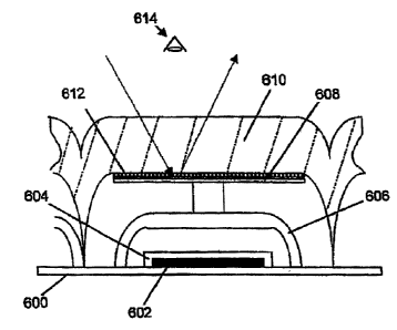
. In the exemplary interferometric modulator shown in FIGS. 5A and 5B,
electrode 502 is
fabricated on substrate 500 and is electrically isolated from membrane/mirror
506 by insulating
film 504. The electrode 502 is disposed opposite the viewing surface and
functions only as an
electrode, not also as a mirror. An optical cavity 505 is formed between
membrane/mirror 506
and secondary mirror 508. Support for secondary mirror 508 is provided by a
transparent
superstructure 510, which can be a thick deposited organic, such as SU-8,
polyimide, or an
inorganic material.
In certain embodiments, with no voltage applied, the membrane/mirror 506
maintains a
certain position shown in FIG. 5A relative to secondary mirror 508, as
determined by the
thickness of the sacrificial layers deposited during manufacture. For an
actuation voltage of about
-13-
CA 02520384 2005-09-20
four volts a thickness of several thousand angstroms might be appropriate. If
the secondary mirror
is made from a suitable material, say chromium, and the mirror/membrane made
from a reflective
material, such as aluminum, then the structure will reflect certain
frequencies of light 511 which
may. be perceived by the viewer 512. In particular, if the chromium is thin
enough to be
semitransparent, about 40 angstroms, and the aluminum is sufficiently thick,
at least 500
angstroms, as to be opaque, then the structure may have a wide variety of
optical responses.
FIGS. 5C and 5D show examples of black and white and color responses,
respectively, for the
exemplary interferometric modulator of FIGS. 5A and 5B. In certain such
embodiments, the
optical response is determined by the cavity length and the thickness of the
constituent layers.
FIG. 5B shows the result of a voltage applied between primary electrode 502
and
membrane/mirror 506 of the exemplary interferometric modulator of FIG. 5A. As
shown in FIG.
513, the membrane/mirror 506 is vertically displaced, thus changing the length
of the optical
cavity and therefore the optical properties of the interferometric modulator.
FIG. 5C shows one
exemplary reflective optical response which is possible with the two states,
illustrating the dark
state 521 when the device is fully actuated, and a white state 523 when the
device is not fully
actuated. FIG. 5D shows an exemplary optical response with color peaks 525,
527, and 529,
corresponding to the colors blue, green, and red respectively. The
electromechanical behavior of
the device in certain embodiments may thus be controlled independently of the
optical
performance. In certain embodiments, the materials and configuration of the
substrate 500, the
primary electrode 502, or the insulating film 504 influence the
electromechanics of the
interferometric modulator but do not appreciably influence the optical
performance of the
interferometric modulator. In certain such embodiments, one or more of these
elements may be
selected independently of the materials comprising the secondary mirror.
In another example of an inverse-type interferometric modulator, shown in FIG.
22A, the
modulator 2200 comprises an opaque substrate 2202, a protective passivation
layer 2222, a
conductor 2204, a dielectric 2206, first support posts 2208, a
mechanical/mirror layer 2210,
second support posts 2212, a metallic mirror 2214, and a transparent layer
2216. A first cavity
2218 is formed between the dielectric 2206 and the mechanical/mirror layer
2210, and a second
cavity 2220 is formed between the mechanical/mirror layer 2210 and the
metallic mirror 2214.
The mechanical/mirror layer 2210 is supported by the first support posts 2208,
and the
transparent layer 2216 is supported by the second support posts 2212. In
certain embodiments,
the conductor 2204 is connected to a driving mechanism and is used for the
electrostatic
displacement of the mechanical/mirror layer 2210. The solid line of the
mechanical/mirror layer
2210 in FIG. 22A shows an undriven or undisplaced condition, whereas the
dotted line of the
mechanical/mirror layer 2210 in FIG. 22A shows a driven or displaced
condition. The
-14-
CA 02520384 2005-09-20
mechanical/mirror layer 2210 is generally selected to produce a desired
optical response to
incident light when it is brought into contact with the dielectric 2206.
In certain embodiments, a viewer 2201 sees an image from a side opposite of
the
substrate 2202. When the mechanical/mirror layer 2210 is subjected to
electrostatic displacement
in certain embodiments, the first cavity 2218 is collapsed and the second
cavity 2220 is
expanded, so that the gap between the metallic mirror layer 2214 and the
mechanical/mirror layer
2210 increases. Other exemplary simple interferometric modulator designs, like
those described
in U.S. Patent No. 6,055,090, achieve a reflective colored state using
interference and a dark state
via absorption. The dark state is achieved in certain such exemplary
interferometric modulators
because the peak of the resulting standing wave is positioned optimally within
the second cavity
2220 to maximize absorption. When the mechanical/mirror 2210 is moved into
contact with, or
much closer to, the dielectric 2206, the standing wave is moved out of
position, reflecting blue,
green, or red light, depending on the predetermined spacing between the
dielectric 2206 and the
mechanical/mirror layer 2210. By narrowing the spacing between the metallic
mirror layer 2214
and the mechanical/mirror layer 2210, the modulator can reflect substantially
all wavelengths in
the visible spectrum, resulting in a reflective white state. As described
above, in certain
embodiments, a viewer 2201 of an inverse interferometric modulator sees an
image from a side
opposite of the substrate, not through the substrate.
In certain embodiments, the substrate comprises a portion of the inverse-type
interferometric modulator which is located opposite to the display side of the
movable mirror and
which does not substantially interact with the light being modulated. As used
herein, the term
"display side" is used to refer to the side of the inverse-type
interferometric modulator from
which the viewer sees the modulated light. The substrate 2202, the conductor
2204, and the
dielectric layer 2206 of FIG. 22A are each below the mechanical/mirror layer
2210, thereby
located opposite to the display side of the mechanical/mirror layer 2210. In
certain embodiments
in which the mechanical/mirror layer 2210 is substantially non-transparent
(e.g., fully reflective),
light impinging on the modulator 2200 from the display side and being
modulated by the
modulator 2200 is not substantially affected by the optical properties of the
substrate 2202, the
conductor 2204, or the dielectric layer 2206. Therefore, in certain
embodiments, at least one of
the substrate 2202, the conductor 2204, and the dielectric layer 2206 can be
chosen to be
substantially non-transparent (e.g., opaque, highly reflective, or
translucent) to light. In certain
embodiments, the substrate 2202 comprises the conductor 2204, the dielectric
layer 2206, or both
the conductor 2204 and the dielectric layer 2206.
Certain embodiments in which at least one of the substrate, the conductor, and
the
dielectric layer of the inverse-type interferometric modulator are non-
transparent provide
advantages not found in other inverse-type interferometric modulators. For
example, typical
-15-
CA 02520384 2005-09-20
inverse-type interferometric modulators have conductive traces on or within
the substrate and
these conductive traces are electrically coupled to the conductor. If the
substrate is substantially
transparent, these conductive traces can appear from the display side to be
"floating" without any
visible supporting structure. When the inverse-type interferometric modulator
is viewed from the
display side, the combination of the conductive traces with the transparent
substrate can produce
a periphery between modulators which appears grey or has moire patterns. In
addition, light
entering the modulator from below (e.g., through a transparent portion of the
substrate) can be
viewed from the display side. Thus, displays utilizing inverse-type
interferometric modulators
having a transparent substrate can exhibit reduced contrast when viewed from
the display side.
Optical masks or mattes can be used to try to avoid this reduced contrast,
however, such
masking requires additional structure and processing steps to be added to the
inverse-type
interferometric modulators. In certain embodiments, the substrate is selected
to be non-
transparent (e.g., opaque, highly reflective, or translucent) so that it
matches the optical
appearance of the conductive traces, thereby providing a uniform periphery
when viewed from
the display side. In certain other embodiments, the substrate is selected to
be non-transparent and
non-reflective (e.g., dark) so that it matches the color of the inverse-type
interferometric
modulator when the modulator is in the dark state. In certain other
embodiments, the substrate is
selected to avoid utilizing mask structures or processing steps.
In certain embodiments, having a non-transparent substrate advantageously
avoids
processing problems due to light scattering during photolithography. In
certain embodiments,
during the fabrication of the inverse-type interferometric modulator,
photolithography techniques
are used to form various features of the modulator. For photolithographic
fabrication of
structures on the substrate, if the substrate is substantially transparent to
the light being used for
the photolithography (e.g., ultraviolet light), then scattering of the light
by features or surfaces
underlying the substrate can result in a diffusion of the photolithography
light. This light
scattering can then affect (e.g., limit the sharpness, precision, or minimum
sizes) the dimensions
of the resulting photolithographically-formed structures. Similarly, a
transparent conductor or a
transparent dielectric layer can generate unwanted scattering of the
photolithography light,
thereby affecting the dimensions of overlaying photolithographically-formed
structures. In
certain embodiments described herein, such scattering is reduced or eliminated
by using a
substrate which is substantially non-transparent to the photolithography
light.
In certain embodiments, having a non-transparent substrate advantageously
shields
underlying circuitry from stray light. In certain embodiments, the inverse-
type interferometric
modulator is fabricated on a semiconductor substrate (e.g., silicon) which
comprises circuitry,
including but not limited to, passive components (e.g., thin-film resistors,
capacitors, inductors),
and active components (e.g., diodes, transistors, integrated circuits). For
example, a silicon
-16-
CA 02520384 2005-09-20
substrate can be fabricated to have capacitive sensing circuitry which can be
scaled to the size of
the interferometric modulator array. In certain embodiments, such sensing
circuitry can be used
to monitor the state of each interferometric modulator in the array (e.g., to
provide memory
capabilities) or to sense external forces applied to the substrate (e.g., to
provide touch-screen
capabilities). In certain other embodiments, the substrate comprises control
circuitry.
If the substrate is transparent, stray light can enter the circuitry of the
substrate. The
stray, light could potentially damage the circuitry or could create charge
carriers in the circuitry,
thereby affecting the noise and accuracy of signals generated by the
circuitry. By using a non-
transparent substrate, the underlying circuitry of the substrate is
substantially protected from stray
light.
In certain embodiments, having a non-transparent substrate advantageously
allows
standard semiconductor processing equipment to be used to fabricate the
interferometric
modulators. For example, for flat-panel display manufacturing using silicon
substrates, various
fabrication steps are dependent on the orientation of the silicon wafer. The
top surface of the
silicon wafer typically has various structures formed thereon so that the
optical properties of the
treated top surface are different from those of the untreated bottom surface
of the silicon wafer.
Existing process equipment uses the different optical properties of the
treated top surface from
the untreated bottom surface to determine the orientation of the silicon
wafer.
It is much more difficult to use this existing process equipment to fabricate
interferometric modulators with a transparent glass substrate. The optical
properties of the top
surface looks substantially the same as that of the bottom surface since the
structures formed on
the top surface are visible from both surfaces. Therefore, glass substrates do
not provide the
different optical properties of the two surfaces which existing process
equipment utilize to
determine orientation of the wafer. To overcome this difficulty in using glass
substrates, various
techniques are required to differentiate between the two surfaces. However,
these techniques can
be cumbersome and difficult to integrate with other fabrication techniques. In
certain
embodiments, by using a non-transparent substrate (e.g., silicon), standard
semiconductor
processing equipment can be easily used to form the interferometric modulators
over the
substrate, since the structures formed on the top surface are no longer
visible from the bottom
surface.
In certain embodiments, having a non-transparent substrate advantageously
allows
integration of the interferometric modulator fabrication with underlying
control circuitry
fabrication. For example, standard semiconductor processing equipment can be
used to form
both the control circuitry in a semiconductor (e.g., silicon) substrate and
the interferometric
modulators on the substrate.
-17-
CA 02520384 2005-09-20
In certain embodiments, having a non-transparent substrate advantageously
increases the
area for control circuitry and advantageously reduces the constraints
associated with integrating
control circuitry within the interferometric modulators. For interferometric
modulators with
control circuitry therein, the control circuitry takes up area which could
otherwise be used for
modulating light, thereby limiting the area of the display which is optically
active. It is therefore
desirable to reduce the portion of the display area taken up by the control
circuitry. By placing
the control circuitry within or on the substrate below the optical components
of the
interferometric modulators, certain embodiments described herein
advantageously remove the
control circuitry from the display area and provide larger areas in which to
form the control
circuitry.
In certain embodiments, having a non-transparent substrate advantageously
facilitates
using illumination sources integrated in the interferometric modulator array.
Incorporating
illumination sources into an interferometric modulator array have previously
been described. For
example, for inverse-type interferometric modulators, the illumination source
(e.g., organic light-
emitting diodes) can be incorporated in the interferometric modulator to
provide illumination
from the display. However, a transparent substrate would provide a pathway for
light from the
illumination source to escape without contributing to the brightness of the
display. In certain
embodiments, at least a portion of the substrate is highly reflective to
reduce the loss of light
from the illumination source through the substrate.
In certain embodiments, an alternative inverse-type interferometric modulator
structure
can be formed using a reflective substrate. FIG. 22B schematically illustrates
another exemplary
inverse-type interferometric modulator 2200 in which the substrate 2202 is
highly reflective. The
mechanical/mirror layer 2210 of FIG. 22B is partially transparent and
partially reflective. For
example, in certain embodiments, the mechanical/mirror layer 2210 comprises a
thin chromium
layer for partially transmitting and reflecting light and a transparent ITO
layer for application of
an appropriate voltage to actuate the interferometric modulator 2200. The
substrate 2202 of FIG.
22B is highly reflective and serves as a stationary reflector. In certain
embodiments, the
interferometric modulator 2200 further comprises a passivation layer 2222 on
the substrate 2202,
a conductor 2204 on the passivation layer 2222, and a dielectric layer 2206 on
the conductor
2204. In certain embodiments, the conductor 2204 comprises a transparent ITO
layer, while in
certain other embodiments, the conductor 2204 comprises a metal with a
passivation layer.
Actuation of the interferometric modulator 2200 by applying appropriate
voltages to the
mechanical/mirror layer 2210 and to the conductor 2204 moves the
mechanical/mirror layer 2210
relative to the substrate 2202, thereby changing the size of the optical
cavity therebetween. In
certain other embodiments, the conductor 2204 is highly reflective and serves
as the stationary
reflector.
-18-
CA 02520384 2005-09-20
As described above, by way of decoupling the interferometric modulator's
optical and
electromechanical performance, in certain embodiments, the inverse
configuration places the
substrate 2202, conductor 2204, and dielectric layer 2206 on the opposite side
of the reflective
mechanical mirror 2210 from the transparent viewing surface 2216, and thus
outside of the
optical path of light interacting with the interferometric modulator.
Accordingly, unlike with
other interferometric modulator designs, the materials used to manufacture the
substrate 2202,
conductor 2204, and dielectric layer 2206 need not have any particular optical
characteristics, but
rather may be comprised of any suitable material.
In certain embodiments, the freedom in the selection of materials used to make
the
substrate 2202, dielectric 2206 and conductor 2204 advantageously provide
improvements in one
or more attributes of the interferometric modulator, including but not limited
to, size, physical
durability, strength, weight, flexibility, cost, manufacturing time/resources,
and
electromechanical performance. For example, in certain embodiments, the
substrate 2202,
dielectric 2206 and/or conductor 2204 can comprise opaque materials that have
superior
structural properties relative to the transparent materials required by prior
interferometric
modulator configurations. For example, materials can be used for the substrate
2202, dielectric
2206 and/or conductor 2204 which have a greater density and/or Young's modulus
than the
transparent materials that were previously required, allowing the use of
stronger and smaller
components in the interferometric modulator. For example, by using a metal
substrate, the
thickness of the substrate, and hence the overall thickness of the
interferometric modulator, can
be advantageously reduced. In addition, a common reason for field returns of
flat-screen displays
is breakage of the glass substrates of these displays. By using stronger and
more durable
materials for the substrate, the lifetimes of the displays are advantageously
increased. In some
embodiments, substrate 2202, dielectric 2206 and/or conductor 2204 are
comprised of materials
having a density greater than 2.5 g/cm3, 3.0 g/cm3, 3.5 g/cm3, 4.0 g/cm3, 5.0
g/cm3, 6.0 g/cm3, or
7.0 g/cm3, and/or having a Young's modulus of greater than 60 gigapascals, 70
gigapascals, 80
gigapascals, 90 gigapascals, 100 gigapascals, 150 gigapascals, 200 gigapascals
or 300
gigapascals.
The substrate of inverse interferometric modulators may be comprised of any
suitable
material, including opaque and translucent materials. Suitable substrate
materials include, but are
not limited to, metals (e.g. stainless steel, aluminum), anodized metals,
silicon (e.g. a silicon
wafer), poly-silicon, plastics, ceramics, polymers (e.g. polyimide, MYLAR ),
carbon (e.g.
graphite), glass, and quartz, as well as alloys and composites of such
materials. In certain
embodiments in which the substrate comprises a flexible plastic or metal foil
material, the
substrate has sufficient flexibility to be used in "roll-to-roll" or "web"
processing in which
electronic circuitry (e.g., thin-film transistors, resistors, capacitors) are
formed on the substrate
-19-
CA 02520384 2005-09-20
(e.g., via deposition or photolithography techniques). In certain such
embodiments, the circuitry
can be fabricated across large areas (e.g. one meter or more in length) and
are compatible for
subsequent fabrication of large interferometric modulator displays. In one
embodiment, the
substrate is an opaque plastic substrate which includes a passivated printed
circuit board. In
certain such embodiments, the passivated printed circuit board can be
fabricated to include the
desired circuitry, and thin-film processing can be used to fabricate the
interferometric modulators
on the passivated printed circuit board. Certain such embodiments
advantageously separate the
circuitry fabrication from the interferometric modulator fabrication. The
substrate may also
comprise a laminate of a plurality of substrate materials. The substrate may
be rigid or flexible.
For example, a flexible substrate may comprise a thin metal or plastic foil.
Although not limited
to the thickness ranges recited herein, the substrate may have a thickness of
about 0.1 millimeter
to about 1.0 millimeter, and more preferably from about 0.3 millimeter to
about 0.7 millimeter. A
thin opaque substrate can be obtained by metal forming operations such as
drawing (e.g.,
stretching a sheet of metal over or through at least one die to make it
thinner).
The substrate is preferably impermeable to moisture and properly passivated.
In various
embodiments, a protective passivation layer is formed on a surface of an
opaque substrate. In
certain embodiments, forming the passivation layer prepares the substrate for
subsequent
processing (e.g., formation of the conductor or dielectric layer). In certain
embodiments in which
a metal substrate is used, the passivation layer provides electrical isolation
to keep other
structures from shorting to the metal substrate. The protective passivation
layer need not be a
separate layer, but can be formed on top of the opaque substrate by
preliminary passivation
treatment. The passivation treatment of certain embodiments includes, but is
not limited to,
removal of exogenous iron or iron compounds from a surface by means of a
chemical dissolution,
most typically by a treatment with an acid solution that will remove the
surface contamination,
but will not significantly affect the opaque substrate itself. Such treatments
include chemical
treatment of an opaque substrate with a mild oxidant, such as a nitric acid
solution, for the
purpose of enhancing the spontaneous formation of a protective passivation
layer. In addition,
the passivation step can include oxide deposition and spin coating of an
organic planarization
layer.
The dielectric layer of inverse interferometric modulators can comprise any
suitable
material known in the art, such as a metal oxide (e.g., aluminum oxide or
silicon dioxide), silicon
nitride, and the like. As described above, the dielectric layer of an inverse
interferometric
modulator need not have any particular optical characteristics, and thus the
structural design and
materials of the dielectric layer can be chosen to optimize its electrical
properties. For example,
the dielectric layer can be comprised of non-transparent (e.g., opaque, highly
reflective, or
translucent materials) that could not otherwise be utilized in other
interferometric modulator
-20-
CA 02520384 2005-09-20
designs. In addition, the dielectric layer in an inverse interferometric
modulator can be
substantially thicker than a dielectric layer of the same material in an
interferometric modulator
in which the dielectric layer effects the optical performance. A dielectric
layer of increased
thickness can improve various aspects of the dielectric layer and/or
interferometric modulator,
such as electrical properties and manufacturing costs. A thicker dielectric
layer can also give
improvements in the range of materials, configurations, and manufacturing
methods that can be
utilized for other layers of the interferometric modulator on the side of the
dielectric layer
opposite from the viewing surface, including the substrate and the conductor.
For example,
electrochemical plating techniques could be used to manufacture the conductor
on the substrate,
followed by deposition of a dielectric layer of enhanced thickness. In various
embodiments, the
dielectric layer of inverse interferometric modulators has a thickness of
greater than about 200
angstroms, 300 angstroms, 400 angstroms, 500 angstroms, 600 angstroms, 700
angstroms, 800
angstroms, 900 angstroms, 1000 angstroms, 2000 angstroms, or several thousand
angstroms.
Inverse type interferometric modulators can be manufactured in various ways,
and can be
applied to various architectures and configurations. For example, inverse-type
interferometric
modulators can be fabricated using semiconductor manufacturing techniques,
such as
photolithography, deposition (e.g., "dry" methods such as chemical vapor
deposition (CVD) and
wet methods such as spin coating), masking, shadow masking, lift-off
processing, and etching
(e.g., dry methods such as plasma etch and wet methods). Examples of suitable
techniques
compatible with embodiments described herein are described in U.S. Pat. No.
6,040,937.
In one embodiment, an inverse-type interferometric modulator, such as that
shown in Fig.
22A, is made by forming a protective passivation layer 2222 on opaque
substrate 2202, and then
forming a conductor 2204 by deposition of electrode material and subsequent
patterning and
etching. The conductor material is conductive and may comprise any suitable
material known in
the art, such as a metal or a semiconductor (such as silicon) doped to have
the desired
conductivity (such as indium tin oxide). In some embodiments, the conductor
and substrate
comprise a printed circuit board. The dielectric 2206 is then formed on the
conductor 2204 by
deposition, preferably by chemical vapor deposition (CVD). Thereafter, a
sacrificial layer (not
shown), which is removed in a later etching step, is deposited. The
sacrificial layer may be any
suitable material known in the art including, but not limited to, molybdenum,
silicon, tungsten, or
titanium. An etch stop is preferably used on top of the sacrificial layer,
which may be a material
that is more resistant to a later etching step than is the sacrificial layer,
and may be a metal (e.g.,
titanium, aluminum, silver, chromium), a dielectric material, preferably a
metal oxide (e.g., an
aluminum oxide), or any other suitable material known in the art. The
sacrificial layer is
patterned and etched using a mask to form the first support posts 2208,
followed by optional
planarization. The mechanical/mirror layer 2210 is then formed by deposition
(followed by
-21-
CA 02520384 2005-09-20
optional planarization). In some embodiments, the mechanical/mirror layer may
comprise silicon
nitride, silicon dioxide, magnesium fluoride, or calcium fluoride as a
substrate on which a
metallic film such as aluminum, silver, or any number of metals is formed on
the order of several
hundred angstroms. The materials can be selected based on spectral properties,
resistive
properties, etc., and can include any material known and used in the art.
Optionally, an insulator
and/or reflection enhancement film, such as metal oxide can be formed.
An etch stop may be formed on top of the mechanical/mirror layer 2210. Another
sacrificial layer is deposited, patterned, and etched to form the second
support posts 2212
(followed by optional planarization). The metallic mirror layer 2214, which
may comprise Cr or
any suitable material known in the art, is deposited and the transparent layer
2216 is deposited
thereon. After the above fabrication, etching with, for example, XeF2 is
conducted to remove the
sacrificial layers. XeF2 is a convenient source of F2 gas. Other etchants
known in the art, such as
F2, may be used in place of or in addition to XeF2.
Another example of an inverse-type interferometric modulator is shown in FIG.
6A. As
with the embodiment shown in FIG. 5, electrode 602 fabricated on substrate 600
is electrically
isolated from membrane/mirror 608 by insulating film 604. The electrode 602 is
disposed
opposite the viewing surface and functions only as an electrode, not also as a
mirror. Unlike the
embodiment shown in FIG. 5, support structure 606 supporting membrane/mirror
608 is
positioned to be hidden by the membrane/mirror 608. In this way, the amount of
inactive area is
effectively reduced, because the viewer 614 sees only the area covered by the
membrane/mirror
608 and the minimum space between adjoining interferometric modulators. This
is unlike the
structure in FIG. 5, where the membrane supports are visible and constitute,
from a color
standpoint, inactive and inaccurate area. FIG. 6A illustrates the structure in
the un-actuated state,
in which membrane/mirror 608 is in contact with secondary mirror 612, which is
supported by
transparent superstructure 610. FIG. 6B reveals the same structure in the
actuated state, in which
membrane/mirror 608 is translated towards insulating film 604, electrode 602,
and substrate 600.
In FIG. 7A, another geometric configuration is illustrated for use in an
interferometric
modulator structure. This design is similar to one shown in U.S. Pat. No.
5,638,084. That design
relied upon an opaque plastic membrane that is anisotropically stressed so
that it naturally resides
in a curled state. Application of a voltage flattens the membrane to provide a
MEMS-based light
shutter.
The device's functionality may be improved by making it interferometric. The
interferometric modulator variation is shown in FIG. 7A, where thin film stack
704 is like the
dielectric/conductor/insulator stack which is the basis for the induced
absorber interferometric
modulator design discussed in U.S. Pat. No. 6,040,937.
-22-
CA 02520384 2005-09-20
Application of a voltage between aluminum membrane 702 and stack 704 in
certain
embodiments causes the membrane 702 to lie flat against the stack. During
fabrication in certain
embodiments, aluminum membrane 702, which could also include other reflective
metals (silver,
copper, nickel), dielectrics, or organic materials which have been undercoated
with a reflective
metal, is deposited on a thin sacrificial layer (not shown) so that it may be
released, using wet
etch or gas phase release techniques. Aluminum membrane 702 is further
mechanically secured
to the substrate 700 by a support tab 716, which is deposited directly on
optical stack 704.
Because of this, light that is incident on the area where the tab and the
stack overlap is absorbed
making this mechanically inactive area optically inactive as well. This
technique eliminates the
need for a separate black mask in this and other interferometric modulator
designs.
In certain embodiments, incident light 706 is either completely absorbed or a
particular
frequency of light 708 is reflected depending on the spacing of the layers of
the stack. The optical
behavior is like that of the induced absorber interferometric modulator
described in U.S. Pat. No.
6,040,937.
FIG. 7B shows the device configuration when no voltage is applied. The
residual stresses
in the membrane 702 in certain embodiments induce it to curl up into a tightly
wound coil. The
residual stresses can be imparted by deposition of a thin layer of material
718 (shown in Fig. 7A)
on top of the membrane 702, which has extremely high residual tensile stress.
Chromium is one
example in which high stresses may be achieved with a film thickness as low as
several hundred
angstroms. With the membrane 702 no longer obstructing its path, light beam
706 is allowed to
pass through the stack 704 (shown in FIG. 7A). The light beam 712 then
intersects with plate
710. Plate 710 can reside in a state of being either highly absorbing, in
which case light beam 712
is absorbed, or highly reflective (of a particular color or white), in which
case light beam 712 is
reflected 714. For the modulator to be used in a reflective display, the
optical stack 704 would be
designed such that, when the device is actuated, it would either reflect a
particular color (if plate
710 were absorbing) or be absorbing (if plate, 710 were reflective).
Rotational Actuation
As shown in FIG. 8A, another interferometric modulator geometry relies on
rotational
actuation. Using the exemplary processes discussed in U.S. Pat. No. 6,040,937,
electrode 802, an
aluminum film about 1000 angstroms thick, and insulator 806 are fabricated on
substrate 800.
Support post 808 and rotational hinge 810 support shutter 812, upon which a
set of reflecting
films 813 has been deposited. The support shutter may be an aluminum film
which is several
thousand angstroms thick. Its X-Y dimensions could be on the order of tens to
several hundred
microns. The films may be interferometric and designed to reflect particular
colors. A fixed
interferometric stack in the form of an induced absorber like that described
in U.S. Pat. No.
6,040,937 would suffice. The films may also comprise polymers infused with
color pigments, or
-23-
CA 02520384 2005-09-20
they may be aluminum or silver to provide broadband reflection. The electrode
802 and the
shutter 812 of certain embodiments are designed such that the application of a
voltage (e.g., 10
volts) between the two causes the shutter 812 to experience partial or full
rotation about the axis
of the hinge 810. Only shutter 818 is shown in a rotated state although
typically all of the shutters
for a given pixel would be driven in unison by a signal on the common bus
electrode 804. Such a
shutter would experience a form of electromechanical hysteresis if the hinges
and electrode
distances were designed such that the electrostatic attraction of the
electrodes overcomes the
spring tension of the hinge at some point during the rotation. The shutters
would thus have two
electromechanically stable states.
In a transmissive mode of operation, the shutter would either block incident
light or allow
it to pass through. FIG. 8A illustrates the reflective mode where incident
light 822 is reflected
back to the viewer 820. In this mode, and in one state, the shutter 812 either
reflects a white light
if the shutter 812 is metallized, or reflects a particular color or set of
colors if it is coated with
interferometric films or pigments. Representative thicknesses and resulting
colors for an
interferometric stack are also described in U.S. Pat. No. 6,040,937. In the
other state, light is
allowed to pass through the shutter 812, where it can be absorbed in substrate
800 if a surface of
the substrate 800 is coated with an absorbing film or films (not shown). These
films could
comprise another pigment infused organic film, or an induced absorber stack
designed to be
absorbing. Conversely, the shutters 812 may be highly absorbing (e.g., black),
and a surface of
the substrate 800 may be coated with highly reflective films 824, or
selectively coated with
pigment or interferometric films to reflect colors, along the lines of the
color reflecting films
described above.
Operation of the device may be further enhanced in certain embodiments by the
addition
of supplementary electrode 814, which provides additional torque to the
shutter when charged to
a potential that induces electrostatic attraction between supplementary
electrode 814 and shutter
812. Supplementary electrode 814 comprises a combination of a conductor 814
and support
structure 816. The electrode may comprise a transparent conductor such as ITO
(indium tin
oxide) that could be about one thousand angstroms thick. All of the structures
and associated
electrodes are preferably machined from materials that are monolithically
deposited on the
surface of a single substrate, and therefore are easily fabricated and
reliably actuated due to good
control over electrode gap spaces. For example, if such an electrode were
mounted on an
opposing substrate, variations in the surface of both the device substrate and
opposing substrate
could combine to produce deviations as much as several microns or more. Thus,
the voltage
required to affect a particular change in behavior could vary by as much as
several tens of volts
or more. Structures that are monolithic follow substrate surface variations
exactly and suffer little
such variation,
-24-
CA 02520384 2005-09-20
FIG. 8B, steps 1-7, shows an exemplary fabrication sequence for the rotational
modulator. In step 1, substrate 830 has been coated with electrode 834 and
insulator 832. Typical
electrode and insulator materials are aluminum and silicon dioxide, each of a
thickness of one
thousand angstroms each. These are patterned in step 2. Sacrificial spacer
836, a material such as
silicon several microns in thickness, has been deposited and patterned in step
3 and coated with
post/hinge/shutter material 838 in step 4. This could be an aluminum alloy or
titanium/tungsten
alloy about 1000 angstroms thick. In step 5, material 838 has been patterned
to form bus
electrode 844, support post 840, and shutter 842. Shutter reflector 846 has
been deposited and
patterned in step 6. In step 7, the sacrificial spacer has been etched away
yielding the completed
structure. Step 7 also reveals a top view of the structure showing detail of
the hinge comprising
support posts 848, torsion arm 850, and shutter 852.
Switching Elements
For certain embodiments comprising interferometric modulators that are binary
devices,
only a small number of voltage levels is required to address a display. The
driver electronics need
not generate analog signals that would be required to achieve gray scale
operation.
Thus, the electronics may be implemented using other means. In particular the
drive
electronics and logic functions can be implemented using switch elements based
on MEMS.
FIGS. 9A through 9E illustrate the concept of certain embodiments. FIG. 9A is
a diagram
of a basic switch building block with an input 900 making a connection to
output 904 by
application of a control signal 902. FIG. 9B illustrates how a row driver
could be implemented.
The row driver for the addressing scheme described above requires the output
of three voltage
levels. Application of the appropriate control signals to the row driver
allows one of the input
voltage levels to be selected for output 912. The input voltages are Vcol1,
Vco10, and Vbias
corresponding to 906, 908, and 910 in FIG. 9B. Similarly, for the column
driver shown in FIG.
9C, the appropriate control signals result in the selection of one or the
other input voltage levels
for delivery to the output 920. The input voltages are Vsel Fl, Vsel FO, and
ground,
corresponding to 914, 916, and 918 in FIG. 9C. FIG. 9D illustrates how a logic
device 932, may
be implemented, in this case a NAND gate, using basic switch building blocks
934, 936, 938, and
940. All of these components can be configured and combined in a way that
allows for the
fabrication of the display subsystem shown in FIG. 9E. The subsystem comprises
controller logic
926, row driver 924, column driver 928, and display array 930, and uses the
addressing scheme
described above in FIG. 3.
Fabrication of the switch elements as MEMS devices makes it possible to
fabricate an
entire display system using a single process. The switch fabrication process
becomes a
subprocess of the interferometric modulator fabrication process and is
illustrated in FIGS. IOA-
10H.
-25-
CA 02520384 2005-09-20
Step I is shown in FIGS. IOA and 10B, which show a side view and top view,
respectively, of the initial stage. Arrow 1004 indicates the direction of the
perspective of the side
view. Substrate 1000 has had sacrificial spacer 1002, a silicon layer
approximately 2000
angstroms thick, deposited and patterned on its surface. In step 2, shown in
FIGS. I OC and IOD
(viewed from the same perspective as FIGS. IOA and 10B), a structural
material, an aluminum
alloy several microns thick, has been deposited and patterned to form source
beam 1010, drain
structure 1008, and gate structure 1006. Several hundred angstroms of a non-
corroding metal
such as gold, iridium or platinum may be plated onto the structural material
at this point to
maintain low contact resistance through the life of the switch. Notch 1012 has
been etched in
source beam 1010 to facilitate the movement of the beam in a plane parallel to
that of the
substrate. Step 3 is illustrated in FIGS. IOE-lOH. FIGS. IOE and lOG depict
front views, with
arrows 1016 indicating the direction of the perspectives, while FIGS. IOF and
IOH depict top
views. In step 3, the sacrificial material has been etched away leaving the
source beam 1010
intact and free to move.
FIG. IOF shows the switch in an un-actuated state 1014. In the actuated state
1018,
shown in FIG. 10H, voltage source 1017 applies a voltage between the source
beam 1010 and the
gate structure 1006 (shown in FIG. IOD), and the source beam 1010 is deflected
towards gate
1006 until it comes into contact with the drain 1008, thereby establishing
electrical contact
between the source beam 1010 and the drain 1008. The mode of actuation is
parallel to the
surface of the substrate, thus permitting a fabrication process that is
compatible with the main
interferometric modulator fabrication processes. In certain embodiments, this
process also
requires fewer steps than processes used to fabricate switches that actuate in
a direction normal
the substrate surface.
FIG. 101 and lOJ illustrates two alternative designs for planar MEMS switches.
The
switch in FIG. 101 differs in that, upon application of a voltage between
switch beam 1028 and
gate structure 1022, switch beam 1028 serves to provide contact between drain
1024 and source
1026. In the switch of FIGS. IOA-IOH, currents that must pass through the
source beam to the
drain may effect switching thresholds, complicating the design of circuits.
This is not the case
with switch shown in FIG. 101. The switch in FIG. 1OJ reveals a further
enhancement. In this
case, insulator 1040 electrically isolates switch beam 1042 from contact beam
1038, which
provides contact between drain 1034 and source 1036 upon application of a
voltage between gate
structure 1032 and switch beam 1042. The insulator 1040 may be a material such
as Si02 that
can be deposited and patterned using conventional techniques. Use of such a
switch eliminates
the need to electrically isolate switch drive voltages from logic signals in
circuits comprising
these switches.
-26-
CA 02520384 2005-09-20
Multidimensional Photonic Structures
In general, interferometric modulators feature elements that have useful
optical properties
and are movable by actuation means with respect to themselves or other
electrical, mechanical or
optical elements.
Assemblies of thin films to produce interferometric stacks are a subset of a
larger class of
structures that we shall refer to as multidimensional photonic structures.
Broadly, we define a
photonic structure as one that has the ability to modify the propagation of
electromagnetic waves
due to the geometry and associated changes in the refractive index of the
structure. Such
structures have a dimensional aspect because they interact with light
primarily along one or more
axes. Structures that are multidimensional have also been referred to as
photonic bandgap
structures (PBG's) or photonic crystals. The text "Photonic Crystals" by John
D. Joannopoulos,
et al. describes photonic structures that are periodic.
A one-dimensional PBG can occur in the form of a thin film stack. By way of
example,
FIG. 16 shows the fabrication and end product of an interferometric modulator
in the form of a
dielectric Fabry-Perot filter. Thin film stacks 1614 and 1618, which could be
alternating layers of
silicon and silicon dioxide each a quarter wave thick, have been fabricated on
a substrate 1600 to
form an interferometric modulator structure that incorporates central cavity
1616. In general, the
stack is continuous in the X and Y direction, but has a periodicity in the
optical sense in the Z
direction due to variations in the refractive index of the materials, as they
are comprised of
alternating layers with high and low indices. This structure can be considered
one-dimensional
because the effect of the periodicity is maximized for waves propagating along
one axis, in this
case the Z-axis.
FIGS. I1A and 11B illustrate two manifestations of a two-dimensional photonic
structure. In FIG. I IA, a microring resonator 1102 can be fabricated from one
of a large number
of well known materials, an alloy of tantalum pentoxide and silicon dioxide
for example, using
well known techniques. For a device optimized for wavelengths in the 1.55 m
range, typical
dimensions are w=1.5 m, h=1.0 m, and r=10 gm.
Fabricated on a substrate 1100 (glass is one possibility though there are many
others), the
structure is essentially a circular waveguide for which the refractive index
and dimensions w, r,
and h determine the frequencies and modes of light which will propagate within
it. Such a
resonator, if designed correctly, can act as a frequency selective filter for
broadband radiation
that is coupled into it. In this case, the radiation is generally propagating
in the XY plane as
indicated by orientation symbol 1101. The one-dimensional analog of this
device would be a
Fabry-Perot filter made using single layer mirrors. Neither device exhibits a
high order optical
periodicity, due to the single layer "boundaries" formed by the mirrors;
however, they can be
considered photonic structures in the broad sense.
-27-
CA 02520384 2005-09-20
A more traditional PBG is shown in FIG. 11B. Columnar array 1106, fabricated
on
substrate 1104, presents a periodic variation in refractive index in both the
X and Y directions.
Electromagnetic radiation propagating through this medium is most
significantly affected if it is
propagating within the XY plane, indicated by orientation symbol 1103.
Because of its periodic nature, the array of FIG. 11B shares attributes with a
one-
dimensional thin film stack, except for its higher-order dimensionality. The
array is periodic in
the sense that along some axis through the array, within the XY plane, the
index of refraction
varies between that of the column material and that of the surrounding
material, which is usually
air. Appropriate design of this array, utilizing variations on the same
principles applied to the
design of thin film stacks, allows for the fabrication of a wide variety of
optical responses
(mirrors, bandpass filters, edge filters, etc.) acting on radiation traveling
in the XY plane. Array
1106 in FIG. 11B includes a singularity or defect 1108 in the form of a column
that differs in its
dimension and/or refractive index. For example, the diameter of this column
might be fractionally
larger or smaller than the remaining columns (which could be on the order of a
quarter
wavelength in diameter), or it may be of a different material (perhaps air vs.
silicon dioxide). The
overall size of the array is determined by the size of the optical system or
component that needs
to be manipulated. The defect may also occur in the form of the absence of a
column or columns
(a row), depending on the desired behavior. This structure is analogous to the
dielectric Fabry-
Perot filter of FIG. 16, but it functions in only two dimensions. In this
case, the defect is
analogous to the cavity 1616 (shown in FIG. 16). The remaining columns are
analogous to the
adjacent two-dimensional stacks.
The relevant dimensions of the structure of FIG. 11B are denoted by column x
spacing
sx, column y spacing sy, (either of which could be considered the lattice
constant), column
diameter d, and array height, h. Like the quarter wave stack, the one-
dimensional equivalent,
column diameters and spacings can be on the order of a quarter wave. The
height, h, is
determined by the desired propagation modes, with little more than one half
wavelength used for
single mode propagation. The equations for relating the size of the structures
to their effect on
light are well known and documented in the text "Photonic Crystals" by John D.
Joannopoulos, et
al.
This kind of structure may also be fabricated using the same materials and
techniques
used to fabricate the resonator 1102 (shown in FIG. 11A). For example, a
single film of silicon
may be deposited on a glass substrate and patterned using conventional
techniques, and etched
using reactive ion etching to produce the high aspect ratio columns. For a
wavelength of 1.55 m,
the diameter and spacing of the columns could be on the order of 0.5 pm and
0.1 m,
respectively.
-28-
CA 02520384 2005-09-20
Photonic structures also make it possible to direct radiation under
restrictive geometric
constraints. Thus, they are quite useful in applications where it is desirable
to redirect and/or
select certain frequencies or bands of frequencies of light when dimensional
constraints are very
tight. Waveguides channeling light propagating in the XY plane may be
fabricated which can
force light to make 90 degree turns in a space less than the wavelength of the
light. This can be
accomplished, for example, by creating the column defect in the form of a
linear row which can
act as the waveguide.
A three-dimensional structure is illustrated in FIG. 12. Three-dimensional
periodic
structure 1202 fabricated on substrate 1200 acts on radiation propagating in
the XY, YZ, and XZ
planes. A variety of optical responses may be attained by appropriate design
of the structure and
selection of its constituent materials. The same design rules apply, however
they are applied
three-dimensionally here. Defects occur in the form of points, lines, or
regions, vs. points and
lines, which differ in size and/or refractive index from the surrounding
medium. In FIG. 12, the
defect 1204 is a single point element, but may also be linear or a combination
of linear and point
elements or regions. For example, a "linear" or "serpentine" array of point
defects may be
fabricated such that it follows an arbitrary three-dimensional path through
the PBG, and acts as a
tightly constrained waveguide for light propagating within it. The defect
would generally be
located internally but is shown on the surface for purposes of illustration.
The relevant
dimensions of this structure are illustrated in the figure. The diameter,
spacing, and materials of
the PBG are completely application dependent, however the aforementioned
design rules and
equations also apply.
Three-dimensional PBGs are more complicated to make. Conventional means for
fabricating one-dimensional or two-dimensional features, if applied in three
dimensions, would
involve multiple applications of deposition, pattern, and etch cycles to
achieve the third
dimension in the structure. Fabrication techniques for building periodic three-
dimensional
structures include: holographic techniques, where a photosensitive material is
exposed to a
standing wave and replicates the wave in the form of index variations in the
material itself; use of
self-organizing organic or self-assembling materials that rely on innate
adhesion and orientation
properties of certain co-polymeric materials to create arrays of columnar or
spherical structures
during the deposition of the material; ceramic approaches that can involve the
incorporation of a
supply of spherical structures of controlled dimensions into a liquid
suspension that, once
solidified, organizes the structures, and can be removed by dissolution or
high temperature;
combinations of these approaches; and other techniques known in the art.
Co-polymeric self-assembly techniques are especially interesting because they
are both
low temperature and require minimal or no photolithography. In general, this
technique involves
the dissolution of a polymer, polyphenylquinoine-block-polystyrene (PPQmPSn)
is one example,
-29-
CA 02520384 2005-09-20
into a solvent such as carbon disulfide. After spreading the solution onto a
substrate and allowing
the solvent to evaporate, a close packed hexagonal arrangement of air filled
polymeric spheres
results. The process can be repeated multiple times to produce multilayers,
and the period of the
array may be controlled by manipulating the number of repeat units of the
components (m and n)
of the polymer. Introduction of a nanometer sized colloid comprising metals,
oxides, or
semiconductors can have the effect of reducing the period of the array
further, as well as
increasing the refractive index of the polymer.
Defects may be introduced via direct manipulation of the material on a
submicron scale
using such tools as focused ion beams or atomic force microscopes. The former
may be used to
remove or add material in very small selected areas or to alter the optical
properties of the
material. Material removal occurs when the energetic particle beam, such as
that used by a
Focused Ion Beam tool, sputters away material in its path. Material addition
occurs when the
focused ion beam is passed through a volatile metal containing gas, such as
tungsten hexafluoride
(for tungsten conductor) or silicon tetrafluoride (for insulating silicon
dioxide). The gas breaks
down, and the constituents are deposited where the beam contacts the
substrate. Atomic force
microscopy may be used to move materials around on a molecular scale.
Another approach involves the use of a technique that can be called micro-
electrodeposition, which is described in detail in U.S. Pat. No. 5,641,391. In
this approach a
single microscopic electrode can be used to define three-dimensional features
of submicron
resolution using a variety of materials and substrates. Metal "defects"
deposited in this way could
be subsequently oxidized to form a dielectric defect around which the PBG
array could be
fabricated using the techniques described above.
The existence of surface features, in the form of patterns of other materials,
on the
substrate upon which the PBG is fabricated may also serve as a template for
the generation of
defects within the PBG during its formation. This is particularly relevant to
PBG processes that
are sensitive to substrate conditions, primarily self-assembly approaches.
These features may
encourage or inhibit the "growth" of the PBG in a highly localized region
around the seed
depending on the specific nature of the process. In this way, a pattern of
defect "seeds" may be
produced and the PBG formed afterwards with the defects created within during
the PBG
formation process.
Thus, the class of devices known as interferometric modulators may be further
broadened
by incorporating the larger family of multidimensional photonic structures
into the modulator
itself. Any kind of photonic structure, which is inherently a static device,
may now be made
dynamic by altering its geometry and/or altering its proximity to other
structures. Similarly, the
micromechanical Fabry-Perot filter (shown in FIG. 16), comprising two mirrors
which are each
one-dimensional photonic structures, may be tuned by altering the cavity width
electrostatically.
-30-
CA 02520384 2005-09-20
FIG. 13 shows two examples of interferometric modulator designs incorporating
two-
dimensional PBGs. In FIG. 13A, a cutaway diagram 1300 reveals a self-
supporting membrane
1304, which has been fabricated with a microring resonator 1306 mounted on the
side facing the
substrate 1303. Waveguides 1301 and 1302 lying within the bulk of the
substrate 1303 are planar
and parallel, and can be fabricated using known techniques. In FIG. 13A, the
interferometric
modulator is shown in the un-driven state with a finite airgap (number)
between the microring
and the substrate. The microring is fabricated so that its position overlaps
and aligns with the
paired waveguides in the substrate below. Dimensions of the microring are
identical to the
example described above in FIG. I IA. Cross-section 1305 shows the dimensions
of the
waveguides, which could be w=1 m, h=0.5 m, and t=100 nm. In the un-driven
state, light 1308
propagates undisturbed in waveguide 1302, and the output beam 1310 is
spectrally identical to
input 1308.
Driving the interferometric modulator to force the microring into intimate
contact with
the substrate and waveguides alters the optical behavior of the device. Light
propagating in
waveguide 1302 may now couple into the microring by the phenomenon of
evanescence. The
microring, if sized appropriately, acts as an optical resonator coupling a
selected frequency from
waveguide 1302 and injecting it into waveguide 1301. This is shown in FIG.
13B, where light
beam 1312 is shown propagating in a direction opposite the direction of input
beam 1308 and
output beam 1310. Such a device may be used as a frequency selective switch
that picks
particular wavelengths out of a waveguide by the application of a voltage or
other driving means
required to bring the structure into intimate contact with the underlying
waveguides. A static
version of this geometry is described in the paper B. E. Little, et al.,
"Vertically Coupled
Microring Resonator Channel Dropping Filter," IEEE Photonics Technology
Letters, vol. 11, no.
2, 1999.
Another example is illustrated in FIG. 13C. In this case, a pair of waveguides
1332 and
1330 and resonator 1314 are fabricated on the substrate in the form of a
columnar PBG. The PBG
is a uniform array of columns, with the waveguides defined by removing two
rows (one for each
waveguide), and the resonator defined by removing two columns. Top view 1333
provides more
detail of the construction of waveguides 1330 and 1332, and the resonator
1314. Dimensions are
dependent on the wavelength of interest as well as materials used. For a
wavelength of 1.55 m,
the diameter and spacing of the columns could be on the order of 0.5 pm and 1
p.m respectively.
The height, h, determines the propagation modes which will be supported and
should be slightly
more than half the wavelength if only single modes are to be propagated.
On the inner surface of the membrane 1315 are fabricated two isolated columns
1311,
which are directed downwards, and have the same dimensions and are of the same
material (or an
optically equivalent material) as the columns on the substrate. The resonator
and columns are
-31-
CA 02520384 2005-09-20
designed to complement each other; there is a corresponding absence of a
column in the resonator
where the column on the membrane is positioned.
When the interferometric modulator is in an undriven state, there is a finite
vertical
airgap 1312, of at least several hundred nanometers between the PBG and the
membrane
columns, and therefore no optical interaction occurs. The absence of columns
in the resonator
acts like defects, causing coupling between waveguides 1330 and 1332. In this
state the device
acts as does the one shown in FIG. 13B, and selected frequencies of light 1328
propagating along
waveguide 1330 are injected into waveguide 1332, and propagate in the opposite
direction 1329
of input beam 1328 and output beam 1326.
Driving the interferometric modulator into contact with the PBG, however,
places the
columns into the resonator, altering its behavior. The defects of the
resonator are eliminated by
the placement of the membrane columns. The device in this state acts as does
the one shown in
FIG. 13A, with light 1328 propagating without interference.
A static version of this geometry is described in the paper H. A. Haus
"Channel drop
filters in photonic crystals," Optics Express, vol. 3, no.1, 1998.
Optical Switches
In FIG. 14A, a device based on the induced absorber includes a self-supporting
aluminum
membrane 1400, on the order of tens to hundreds of microns square, which is
suspended over a
stack of materials 1402, comprising a combination of metals and oxides
patterned on transparent
substrate 1404. The films utilized in the induced absorber modulator,
described in U.S. Pat. No.
6,040,937, could serve this purpose. The films on the substrate may also
comprise a transparent
conductor, such as ITO (indium tin oxide). The structure may incorporate on
its underside a
glossy metal film, such as molybdenum or tungsten, of several hundred
angstroms in thickness.
The materials of certain embodiments are configured so that in the undriven
state the
device reflects in a particular wavelength region, but becomes very absorbing
when the
membrane is driven into contact. Side view 1410 shows a view of the device
looking into the side
of the substrate 1412. Light beam 1408 propagates at some arbitrary angle
through the substrate
1412 and is incident on interferometric modulator 1406, shown in the un-driven
state. Assuming
the frequency of the light corresponds with the reflective region of the
interferometric modulator
in the un-driven state, the light is reflected at a complementary angle 1411
and propagates away.
Side view, 1414, shows the same interferometric modulator in the driven state.
Because the
device is now very absorbing, the light which is incident upon it is no longer
reflected but
absorbed by the materials in the interferometric modulator's stack.
Thus, in this configuration, the interferometric modulator may act as an
optical switch for
light that is propagating within the substrate upon which it is fabricated.
The substrate is
machined to form surfaces that are highly polished, highly parallel (to within
1/10 of a
-32-
CA 02520384 2005-09-20
wavelength of the light of interest), and many times thicker (at least
hundreds of microns) than
the wavelength of light. This allows the substrate to act as a
substrate/waveguide in that light
beams propagate in a direction which is, on average, parallel to the substrate
but undergo multiple
reflections from one surface to another. Light waves in such a structure are
often referred to as
substrate guided waves.
FIG. 14B shows a variation on this theme. Membrane 1422 is patterned on
substrate 1426
over optical stack 1424 such that the membrane 1422 is no longer rectangular
but is tapered
towards one end 1420. While the mechanical spring constant of the structure
remains constant
along its length, the electrode area decreases. Thus, the amount of force
which can be applied
electrostatically is lower at the narrower end 1420 of the taper. If a
gradually increasing voltage
is applied, the membrane 1422 will begin to actuate at the wider end first and
actuation will
progress along arrow 1428 as the voltage increases.
To incident light, the interferometric modulator operates as an absorbing
region with an
area that depends on the value of the applied voltage. Side view 1434 shows
the effect on a
substrate propagating beam when no voltage is applied. The corresponding
reflective area 1429
in view 1435, which shows the interferometric modulator from the perspective
of the incident
beam, shows "footprint" 1431 of the beam superimposed on the reflective area
1429. Since the
entire reflective area 1429 is non-absorbing, beam 1430 is reflected from
interferometric
modulator 1428 (with minimal losses) in the form of beam 1432.
In side view 1436, an interim voltage value is applied and the reflected beam
1440 has
been attenuated to some extent because the reflective area 1429 shown in view
1437 is now
partially absorbing. Views 1438 and 1439 reveal the result of full actuation
and the complete
attenuation of the beam because the reflective area 1429 is completely
absorbing.
Thus, by using a tapered geometry, a variable optical attenuator may be
created, the
response of which is directly related to the value of the applied voltage.
Another kind of optical switch is illustrated in FIG. 15A. Support frame 1500
is
fabricated from a metal, such as aluminum several thousand angstroms in
thickness, in such a
way that it is electrically connected to mirror 1502. Mirror 1502 resides on
transparent optical
standoff 1501, which is bonded to support 1500. Mirror 1502 may comprise a
single metal film or
combinations of metals, oxides, and semiconducting films.
The standoff 1501 is fabricated from a material that has the same or higher
index of
refraction than that of the substrate 1504. This could be SiO2 (same index) or
a polymer with a
variable index. The standoff 1501 is machined so that the mirror 1502 is
supported at an angle of
45 degrees. Machining of the standoff 1501 can be accomplished using a
technique known as
analog lithography that relies on a photomask with features that are
continuously variable in
terms of their optical density. By appropriate variation of this density on a
particular feature,
-33-
CA 02520384 2005-09-20
three-dimensional shapes can be formed in a photoresist that is exposed using
this mask. The
shape can then be transferred into other materials via reactive ion etching.
The entire assembly is
suspended over conductor 1503 which has been patterned to provide an
unobstructed "window"
1505 into the underlying substrate 1504. That is to say, the bulk of conductor
1503 has been
etched away so that window 1505, comprising bare glass, is exposed. The
switch, like other
interferometric modulators, can be actuated to drive the whole assembly into
contact with the
substrate/waveguide. Side view, 1512, shows the optical behavior. Beam 1510 is
propagating
within the substrate at an angle 45 degrees from normal that prevents it from
propagating beyond
the boundaries of the substrate. This is because 45 degrees is above the
angle, known as the
critical angle, which allows the beam to be reflected 1508 with minimal or no
losses at the
interface 1519 between the substrate and the outside medium by the principle
of total internal
reflection (TIR).
The principle of TIR depends on Snell's law, but a basic requirement is that
the medium
outside the substrate must have an index of refraction that is lower than that
of the substrate. In
side view 1512, the device is shown with the switch 1506 in the un-driven
state, and beam 1510
propagating in an unimpeded fashion. When, as shown in side view 1514, switch
1506 is actuated
into contact with the substrate 1516, the beam's path 1518 is altered. Because
the standoff has a
refractive index greater than or equal to that of the substrate 1516, the beam
no longer undergoes
TIR at the interface. The beam propagates out of the substrate 1516 into the
optical standoff,
where it is reflected by the mirror. The mirror is angled at 45 degrees, such
that the reflected
beam 1518 is now traveling at an angle which is normal to the plane of the
substrate. The result is
that the light may propagate through the substrate interface because it no
longer meets the criteria
for TIR, and can be captured by a fiber coupler 1520, which has been mounted
on the opposite
side of the substrate/waveguide. A similar concept is described in the paper,
X. Zhou, et al.,
"Waveguide Panel Display Using Electromechanical Spatial Modulators," SID
Digest, vol.
XXIX, 1998. This particular device was designed for emissive display
applications. The mirror
may also be implemented in the form of a reflecting grating, which may be
etched into the
surface of the standoff using conventional patterning techniques. This
approach, however,
exhibits wavelength dependence and losses due to multiple diffraction orders
that are not an issue
with thin film mirrors. Additionally, alternative optical structures may be
substituted for the
mirror, with their respective attributes and shortcomings. These can be
categorized as refractive,
reflective, and diffractive, and can include micro-lenses (both transmissive
and reflective),
concave or convex mirrors, diffractive optical elements, holographic optical
elements, prisms,
and any other form of optical element which can be created using micro-
fabrication techniques.
In the case where an alternative optical element is used, the standoff and the
angle it imparts to
the optic may not be necessary, depending on the nature of the micro-optic.
-34-
CA 02520384 2005-09-20
This variation on the interferometric modulator acts as a de-coupling switch
for light.
Broadband radiation, or specific frequencies if the mirror is designed
correctly, can be coupled
out of the substrate/waveguide at will. Side view 1526 shows a more elaborate
implementation in
which an additional fixed mirror 1528, angled at 45 degrees, has been
fabricated on the side of
the substrate 1524 opposite that of the de-coupling switch 1506. This mirror
differs from the
switch in that it cannot be actuated. By careful selection of the angles of
the mirrors on both
structures, light 1522 that has been effectively decoupled out of the
substrate 1524 by switch
1506 may be recoupled back into the substrate (dashed lines) by re-coupling
mirror 1528.
However, by fabricating the recoupling mirror 1528 with different orientations
in the XY plane,
the mirror combination may be used to redirect light in any new direction
within the
substrate/waveguide. The combination of these two structures will be referred
to as a directional
switch. Re-coupling mirrors can also be used to couple any light that is
propagating into the
substrate in a direction normal to the surface.
FIG. 15B shows one implementation of an array of directional switches. Looking
down
onto the substrate 1535, linear array 1536 is an array of fiber couplers which
directs light into the
substrate 1535 at an angle normal to the XY plane. An array of re-coupling
mirrors (not visible)
is positioned directly opposite the fiber coupler array to couple light into
the substrate 1535. On
the surfaces of the substrate 1535 are fabricated an array of directional
switches, of which 1531 is
a representative example. The switches are positioned in a way such that light
coupled into the
substrate from any one of the input fiber couplers 1536 may be directed to any
one of the output
fiber, couplers 1532. In this way, the device may act as an N X N optical
switch that can switch
any one of any number of different inputs to any one of any number of
different outputs.
Tunable Filter
Returning to FIG. 16, an interferometric modulator in the form of a tunable
Fabry-Perot
filter is shown. In this case, conducting contact pad 1602 has been deposited
and patterned on
substrate 1600, along with dielectric mirrors 1604 and 1608 and sacrificial
layer 1606. This may
consist of a silicon film with a thickness of some multiple of one-half a
wavelength. The mirrors
may comprise stacks of materials, Ti02 (high index) and Si02 (low index) being
two examples,
with alternating high and low indices. One of the layers may also be air.
Insulating layer 1610 is
deposited and patterned such that second contact pad 1612 only contacts mirror
1608. Mirror
1608 is subsequently patterned leaving a mirror "island" 1614 connected by
supports 1615. The
lateral dimensions of the island are primarily determined by the size of the
light beam with which
it will interact. This is usually on the order of tens to several hundred
microns. Sacrificial layer
1606 is partially etched chemically, but in a manner leaving standoffs 1613 of
sufficient size to
provide mechanical stability, probably on the order of tens of microns square.
If the top layer of
mirror 1608 and the bottom layer of mirror 1604 are lightly doped to be
conducting, then
-35-
CA 02520384 2005-09-20
application of a voltage between contact pads 1602 and 1612 will cause the
mirror island to be
displaced. Thus, the structure's optical response may be tuned.
FIG. 17A shows an application of this tunable filter. On the top surface of
substrate 1714
has been fabricated tunable filter 1704, mirrors 1716, and anti-reflection
coating 1712. A mirror
1717 has also been fabricated on the bottom surface of the substrate, e.g.,
from a metal such as
gold of at least 100 nm thick. Mounted on the top surface of the substrate is
an optical
superstructure, 1706, whose inner surface is at least 95% reflective, e.g., by
the addition of a
reflecting gold film, and which also supports an angled mirror 1710. In this
device, light beam
1702 propagates within the substrate at some angle that is larger than the
critical angle, which is
approximately 41 degrees for a substrate of glass and a medium of air.
Therefore, the mirrors
1716 are required to keep the beam 1702 bounded within the confines of the
substrate/waveguide.
This configuration allows greater flexibility in the selection of angles at
which the light
propagates.
Beam 1702 is incident upon Fabry-Perot filter 1704, which transmits a
particular
frequency of light 1708 while reflecting the rest 1709. The transmitted
frequency 1708 is incident
onto.and reflected from the reflective superstructure 1706, and reflected
again by mirror 1716
onto angled mirror 1710. Mirror 1710 is tilted such that the light transmitted
by filter 1704 is
directed towards antireflection coating 1712 at a normal angle with respect to
the substrate 1714,
and passes through the substrate 1714 and into the external medium. The
reflected frequency
1709 is reflected within the substrate 1714 between mirrors 1717 and 1716, and
finally reflected
1718 through the substrate 1714 and into the external medium. The device as a
whole thus acts
as a wavelength selective filter.
The superstructure may be fabricated using a number of techniques. One would
include
the bulk micromachining of a slab of silicon to form a cavity of precise
depth, e.g., on the order
of the thickness of the substrate and at least several hundred microns. The
angled mirror is
fabricated after etching of the cavity, and the entire assembly is bonded to
the substrate, glass for
example, using any one of many silicon/glass bonding techniques.
FIG. 17B is a more elaborate version. In this example, a second tunable filter
1739 has
been added to provide an additional frequency selection channel, which allows
two separate
frequencies to be selected independently. Beam 1730 passes through substrate
1744 and is
incident upon a first Fabry-Perot filter 1732, which transmits a particular
frequency of light 1734
while reflecting the rest. The transmitted frequency 1734 is incident onto and
reflected from
mirror 1736, and reflected again by a second mirror onto one of two detectors
1738. The
reflected frequency is reflected within the substrate 1744, between mirror
1740 and an additional
mirror onto a second Fabry-Perot filter 1739, which transmits a particular
frequency of light and
reflects the rest through the substrate 1744 and into the external medium. The
frequency
-36-
CA 02520384 2005-09-20
transmitted by the second filter 1739 is reflected between reflective
superstructure 1742 and an
additional mirror onto detector 1738. Detectors 1738 allow for a higher degree
of integrated
functionality.
FIG. 17C incorporates integrated circuits. Light beam 1750 has been coupled
into
substrate 1770 and is incident upon tunable filter 1752. This filter is
different than those of FIGS.
17A and 17B in that it includes recoupling mirror 1756 that has been
fabricated on the surface of
the movable mirror of the filter. The angle of the mirror is such that the
frequency selected by
filter 1752 is now coupled directly back into the substrate at a normal angle
in the form of light
beam 1758. The remaining frequencies contained in light beam 1750 propagate
until they
encounter recoupling mirror 1760 which is angled so that it presents a surface
which is
perpendicular to the propagating beam. The beam thus retraces its path back
out of the device
where it may be used by other devices that are connected optically. Light beam
1758 is incident
on IC 1764 that can detect and decode the information within the beam. The IC
1764 may be in
the form of an FPGA or other silicon, silicon/germanium, or gallium arsenide-
based integrated
circuit that could benefit from being directly coupled to information carrying
light. For example,
a high bandwidth optical interconnect may be formed between ICs 1764 and 1762
by virtue of the
bidirectional light path 1772. This is formed by a combination of mirrors 1776
and 1778, and
recoupling mirrors 1768. Light can be emitted by either ICs if they
incorporate components such
as vertical cavity surface emitting lasers (VCSELS) or light emitting diodes
(LEDs). Light can be
detected by any number of optically sensitive components, with the nature of
the component
depending on the semiconductor technology used to fabricate the IC. Light that
is incident on the
IC may also be modulated by interferometric modulators that have been
fabricated on the surface
of the IC that is exposed to the substrate propagating light.
Optical mixer using substrate waveguide
FIGS. 18A and 18B are an illustration of a two-channel optical mixer
implemented using
a TIR version of a substrate/waveguide. FIG. 18A shows a schematic of the
device. Light
containing multiple wavelengths has two particular wavelengths, 1801 and 1803,
split off and
directed towards two independent variable attenuators 1805. They are then
output to several
possible channels 1807 or into an optical stop 1813.
FIG. 18B reveals an implementation. The input light is directed into the
device through
fiber coupler 1800, through anti-reflection coating 1802, and coupled into
substrate 1804 using
re-coupling mirror 1806. The recoupling mirror directs the light onto tunable
filter 1808, splitting
off frequency kl and directing all non-selected frequencies 1814 toward a
second tunable filter
1809, which splits off frequency X2, with the remaining frequencies (beam
1819) propagating
further downstream via TIR. Following the path of frequency Al, which was
transmitted by
tunable filter 1808, the light is redirected (beam 1815) back into the
substrate waveguide via
-37-
CA 02520384 2005-09-20
mirror 1810, through an AR coating, and re-coupled back into substrate 1804 by
re-coupling
mirror 1811, which directs beam 1815 towards attenuator 1812. Frequency A.2,
which was
transmitted by the second tunable filter 1809, is redirected (beam 1817) into
substrate 1804 by a
mirror positioned similarly to mirror 1810, where it follows a path parallel
to beam 1815. Beams
1815 and 1817 propagate within substrate 1804 by TIR, and are positionally
shifted by virtue of
beam repositioner 1816.
Beam repositioner 1816 produces the same result as a recoupling mirror, except
that the
mirror is parallel to the surface of the substrate. Because the mirror is
suspended a fixed distance
beyond the substrate surface, the position of the point of incidence on the
opposite substrate
interface is shifted towards the right. This shift is directly determined by
the height of the
repositioner. The beam 1819, containing wavelengths unselected by the second
tunable filter
1809, is also shifted by virtue of repositioner 1818. The result is that all
three beams (1815, 1817,
and 1819) are equally separated when they are incident on an array of
decoupling switches 1820
and 1824. These serve to selectively redirect the beams into one of two
optical combiners, 1828
being one of them, or into detector/absorber 1830. The optical combiners
direct light from
decoupling switches 1820 and 1824 into output fiber couplers 1822 and 1826,
respectively. The
optical combiners may be fabricated using a variety of techniques. A polymeric
film patterned
into the form of a pillar with its top formed into a lens using reactive ion
etching is one approach.
The absorber/detector, comprising a semiconductor device that has been bonded
to the substrate,
serves to allow the measurement of the output power of the mixer. Optical
superstructures 1829
support external optical components and provide a hermetic package for the
mixer.
The combination of planar interferometric modulators and a substrate waveguide
provide
a family of optical devices that are easily fabricated, configured, and
coupled to the outside world
because the devices reside on the waveguide and/or on the superstructure and
are capable of
operating on light which is propagating within the waveguide, and between the
waveguide and
the superstructure. Because all of the components are fabricated in a planar
fashion, economies of
scale can be achieved by bulk fabrication over large areas, and the different
pieces may be
aligned and bonded easily and precisely. In addition, because all of the
active components exhibit
actuation in a direction normal to the substrate, they are relatively simple
to fabricate and drive
compared to more elaborate non-planar mirrors and beams. Active electronic
components may be
bonded to either the superstructure or the substrate/waveguide to increase
functionality.
Alternatively, active devices may be fabricated as a part of the
superstructure, particularly if it is
a semiconductor such as silicon or gallium arsenide.
Printing Style Fabrication Processes
Because they are planar and because many of the layers do not require
semiconducting
electrical characteristics that require specialized substrates,
interferometric modulators, as well as
-38-
CA 02520384 2005-09-20
many other MEMS structures, may take advantage of manufacturing techniques
which are akin to
those of the printing industry. These kinds of processes typically involve a
"substrate" which is
flexible and in the form of a continuous sheet, for example of paper or
plastic. Referred to as web
fed processes, they usually involve a continuous roll of the substrate
material which is fed into a
series of tools, each of which selectively coats the substrate with ink in
order to sequentially build
up a full color graphical image. Such processes are of interest due to the
high speeds with which
products can be produced.
FIG. 19 is a representation of such a sequence applied to the fabrication of a
single
interferometric modulator and, by extension, to the fabrication of arrays of
interferometric
modulators or other microelectromechanical structures. Web source 1900 is a
roll of the substrate
material, such as transparent plastic. A representative area 1902 on a section
of material from the
roll contains, for the purposes of this description, only a single device.
Embossing tool 1904
impresses a pattern of depressions into the plastic sheet. This can be
accomplished by a metal
master which has the appropriate pattern of protrusions etched on it.
The metal master is mounted on a drum that is pressed against the sheet with
enough
pressure to deform the plastic to form the depressions. View 1906 illustrates
this. Coater 1908
deposits thin layers of material using well known thin film deposition
processes, such as
sputtering or evaporation. The result is a stack 1910 of four films comprising
an oxide, a metal,
an oxide, and a sacrificial film. These materials correspond to the induced
absorber
interferometric modulator design. A tool 1912 dispenses, cures, and exposes
photoresist for
patterning these layers. Once the pattern has been defined, the film etching
occurs in tool 1914.
Alternatively, patterning may be accomplished using a process known as laser
ablation. In this
case, a laser is scanned over the material in a manner that allows it to be
synchronized with the
moving substrate. The frequency and power of the laser is such that it can
evaporate the materials
of interest to feature sizes that are on the order of microns. The frequency
of the laser is tuned so
that it only interacts with the materials on the substrate and not the
substrate itself. Because the
evaporation occurs so quickly, the substrate is heated only minimally.
In this device example, all of the films are etched using the same pattern.
This is seen in
1918 where the photoresist has been stripped away after the application of
tool 1916. Tool 1920
is another deposition tool that deposits what will become the structural layer
of the
interferometric modulator. Aluminum is one candidate for this layer 1922. This
material may also
include organic materials which exhibit minimal residual stress and which may
be deposited
using a variety of PVD and PECVD techniques. This layer is subsequently
patterned, etched, and
stripped of photoresist using tools 1924, 1926, and 1928 respectively. Tool
1930 is used to etch
away the sacrificial layer. If the layer is silicon, this can be accomplished
using XeF2, a gas
-39-
CA 02520384 2005-09-20
phase etchant used for such purposes. The result is the self-supporting
membrane structure 1932
that forms the interferometric modulator.
Packaging of the resulting devices is accomplished by bonding flexible sheet
1933 to the
top surface of the substrate sheet. This is also supplied by a continuous roll
1936 that has been
coated with a hermetic film, such as a metal, using coating tool 1934. The two
sheets are joined
using bonding tool 1937, to produce the resulting packaged device 1940.
Stress Measurement
Residual stress is a factor in the design and fabrication of MEMS structures.
In
interferometric modulators, and other structures in which structural members
have been
mechanically released during the fabrication process, the residual stress
determines the resulting
geometry of the member.
The interferometric modulator, as an interferometric device, is sensitive to
variations in
the resulting geometry of the movable membrane. The reflected, or in other
design cases
transmitted, color is a direct function of the airgap spacing of the cavity.
Consequently, variations
in this distance along the length of a cavity can result in unacceptable
variations in color. On the
other hand, this property is a useful tool in determining-the residual stress
of the structure itself,
because variations in color can be used to determine the variations and degree
of deformation in
the membrane. Knowing the deformed state of any material allows for a
determination of the
residual stresses in the material. Computer modeling programs and algorithms
can use two-
dimensional data on the deformation state to determine this. Thus, the
interferometric modulator
structure can provide a tool for making this assessment.
FIGS. 20A-20F show examples of how an interferometric modulator may be used in
this
fashion. Interferometric modulators 2000 and 2002 in FIG. 20A, 2004 and 2006
in FIG. 20C, and
2008 and 2010 in FIG. 20E are shown from a side perspective, while the same
interferometric
modulators are shown from a bottom perspective viewed through the substrate in
FIGS. 20B,
20D, and 20F, respectively. The interferometric modulators on the left are of
a double cantilever
form and the interferometric modulators on the right are of single cantilever
form. In the case of
FIG. 20A, the structural materials have no residual stresses, and both
membranes exhibit no
deformation. As shown in FIG. 20B, the devices, as viewed through the
substrate, exhibit a
uniform color that is determined by the thickness of the spacer layer upon
which they were
formed. Interferometric modulators 2004 and 2006 in FIG. 20C are shown with a
stress gradient
that is more compressive on the top than it is on the bottom. The structural
membranes exhibit a
deformation as a result, and the nature of the color change is revealed in the
bottom view in FIG.
20D. Color region 2018, corresponding to the middle region of the membrane of
interferometric
modulator 2004, might be red because it is farther away from the substrate
than the regions of the
membrane flanking region 2018. Conversely, if color region 2016, corresponding
to the portion
-40-
CA 02520384 2005-09-20
of membrane of the left side of interferometric modulator 2006, were green,
then color region
2014, corresponding to the portion of membrane of the right side of
interferometric modulator
2006, might be blue, because it is closer to the substrate.
Interferometric modulators 2008 and 2010 in FIG. 20E are shown in a state
where the
stress gradient exhibits higher tensile stress on the top than on the bottom.
The structural
members are deformed accordingly, resulting in a color change as shown in the
bottom view of
FIG. 20F. In this case, region 2024, corresponding to the middle portion of
the membrane of
interferometric modulator 2008, may be blue, while the portions of the
membrane flanking region
2024, corresponding to the outer portions of the membrane of interferometric
modulator 2008,
may ' be green, since they are further away from the substrate. Likewise, if
region 2020,
corresponding to the left side of the membrane of interferometric modulator
2010, is red, region
2022, corresponding to the right side of the membrane of interferometric
modulator 2010, might
be blue, as it is farther away from the substrate.
In FIG. 20G, a system is shown which can be used to quickly and accurately
assess the
residual stress state of a deposited film. Wafer 2030 comprises an array of
interferometric
modulator structures consisting of both single and double cantilevered
membranes with varying
lengths and widths. The structural membranes are fabricated from a material
whose mechanical
and residual stress properties are well characterized. Many materials are
possible, subject to the
limitations of the requisite reflectivity that can be quite low given that the
interferometric
modulators in this case are not to be used for display purposes. Good
candidates would include
materials in crystalline form (e.g., silicon, aluminum, germanium), which are
or can be made
compatible from a fabrication standpoint, exhibit some degree of reflectivity,
and have
mechanical properties that are or can be characterized to a high degree of
accuracy. These "test
structures" are fabricated and released so that they are freestanding. If the
materials are without
stress, then the structures should exhibit no color variations. Should this
not be the case, however,
then the color states or color maps may be recorded by use of a high
resolution imaging device
2034, which can obtain images of high magnification via optical system 2032.
The imaging device is connected to a computer system 2036, upon which resides
hardware capable of recording and processing the image data. The hardware
could comprise
readily available high speed processing boards to perform numerical
calculations at high rates of
speed. The software may consist of collection routines to collect color
information and calculate
surface deformations. The core routine would use the deformation data to
determine the optimal
combination of uniform stress and stress gradient across the thickness of the
membrane, which is
capable of producing the overall shape.
One mode of use could generate a collection of "virgin" test wafers with
detailed records
of their non-deposited stress states, to be put away for later use. When the
need arises to
-41-
CA 02520384 2005-09-20
determine the residual stress of a deposited film, a test wafer is selected
and the film is deposited
on top of it. The deposited film alters the geometry of the structures, and
consequently their color
maps. Using software resident on the computer system, the color maps of the
test wafer both
before and after may be compared, and an accurate assessment of the residual
stress in the
deposited film made. The test structures may also be designed to be actuated
after deposition.
Observation of their behavior during actuation with the newly deposited films
can provide even
more information about the residual stress states, as well as the change in
the film properties over
many actuation cycles.
This technique may also be used to determine the stress of films as they are
being
deposited. With appropriate modification of the deposition system, an optical
path may be
created allowing the imaging system to view the structures and track the
change of their color
maps in real time. This would facilitate real-time feedback systems for
controlling deposition
parameters in an attempt to control residual stress in this manner. The
software and hardware
may "interrogate" the test wafer on a periodic basis and allow the deposition
tool operator to alter
conditions as the film grows. Overall, this system is superior to other
techniques for measuring
residual stress, which either rely on electromechanical actuation alone, or
utilize expensive and
complex interferometric systems to measure the deformation of fabricated
structures. The former
suffers from a need to provide drive electronics to a large array of devices,
and inaccuracies in
measuring displacement electronically. The latter is subject to the optical
properties of the films
under observation, and the complexity of the required external optics and
hardware.
Discontinuous Films
Another class of materials with interesting properties are films whose
structure is-not
homogeneous. These films can occur in several forms and we shall refer to them
collectively as
discontinuous films. FIG. 21 A illustrates one form of a discontinuous film.
Substrate 2000 could
be a metal, dielectric, or semiconductor, which has had contours 2104, 2106,
and 2108 etched
into its surface. The contours, comprising individual structural profiles
which should have a
height 2110 that is some fraction of the wavelength of light of interest, are
etched using
photolithographic and chemical etching techniques to achieve profiles which
are similar to those
illustrated by, 2104 (triangular), 2106, (cylindrical) and 2108 (klopfenstein
taper). The effective
diameter of the base 2102 of any of the individual profiles is also on the
order of the height of the
pattern. While each contour is slightly different, they all share in common
the property that as
one traverses from the incident into the substrate, the effective index of
refraction goes gradually
from that of the incident medium to that of the film substrate 2000 itself.
Structures of this type
act as superior antireflection coatings, compared to those made from
combinations of thin films,
because they do not suffer as much from angular dependencies. Thus, they
remain highly
antireflective from a broader range of incident angles.
-42-
CA 02520384 2005-09-20
FIG. 21B reveals a coating 2120 that has been deposited on substrate 2122 and
could also
be of a metal, dielectric, or semiconductor. The film, in this case, is still
in the early stages of
formation, somewhere below 1000 angstroms in thickness. During most deposition
processes,
films undergo a gradual nucleation process, forming material localities that
grow larger and
larger until they begin to join together and, at some point, form a continuous
film. FIG. 21C
shows a top view of film 2124. The optical properties of films in the early
stage differ from that
of continuous films. For metals, a discontinuous film tends to exhibit higher
losses than its
continuous equivalent.
FIG. 21D illustrates a third form of discontinuous film. In this case, film
2130 has been
deposited on substrate 2132 to a thickness, at least a thousand angstroms,
such that it is
considered continuous. A pattern of "subwavelength" (having a diameter smaller
than the
wavelength of interest) holes 2134 is produced in the material using
techniques which are similar
to the self-assembly approach described earlier. In this case, the polymer can
act as a mask for
transferring the etch pattern into the underlying material, and the holes can
be etched using
reactive ion etch techniques. Because the material is continuous, but
perforated, it does not act
like the early stage film of FIG. 21 B. Instead, its optical properties differ
from the un-etched film
in that incident radiation experiences lower losses and may exhibit
transmission peaks based on
surface plasmons. Additionally, the geometry of the holes, as well as the
angle of incidence and
refractive index of the incident medium, may be manipulated to control the
spectral
characteristics of the light that is transmitted. FIG. 21E shows a top view of
the perforated film
2136. Films such as these are described in the paper "Control of optical
transmission through
metals perforated with subwavelength hole arrays" by Tae Jin Kim. While they
are regular in
structure, they differ from PBGs.
All three of these types of discontinuous films are candidates for inclusion
into an
interferometric modulator structure. That is to say they could act as one or
more of the material
films in the static and/or movable portions of an interferometric modulator
structure. All three
exhibit unique optical properties which can be manipulated in ways that rely
primarily on the
structure and geometry of the individual film instead of a combination of
films with varying
thickness. They can be used in conjunction with other electronic, optical, and
mechanical
elements of an interferometric modulator that they could comprise. In very
simple cases, the
optical properties of each of these films may be changed by bringing them into
direct contact or
close proximity to other films via surface conduction or optical interference.
This can occur by
directly altering the conductivity of the film, and/or by altering the
effective refractive index of
its surrounding medium. Thus more complex optical responses in an individual
interferometric
modulator may be obtained with simpler structures that have less complex
fabrication processes.
-43-
CA 02520384 2005-09-20
Visual Display Devices
Additional embodiments of the instant invention include visual display devices
comprising a plurality of interferometric modulator devices fabricated in a
large array so as to
form pixels within a reflective display. Figures 23A and 23B are system block
diagrams
illustrating an embodiment of a display device 40. The display device 40 can
be, for example, a
cellular or mobile telephone. However, the same components of display device
40 or slight
variations thereof are also illustrative of various types of display devices
such as televisions and
portable media players.
The display device 40 includes a housing 41, a display 30, an antenna 43, a
speaker 44,
an input device 48, and a microphone 46. The housing 41 is generally formed
from any of a
variety of manufacturing processes as are well known to those of skill in the
art, including
injection molding, and vacuum forming. In addition, the housing 41 may be made
from any of a
variety of materials, including but not limited to plastic, metal, glass,
rubber, and ceramic, or a
combination thereof. In one embodiment the housing 41 includes removable
portions (not
shown) that may be interchanged with other removable portions of different
color, or containing
different logos, pictures, or symbols.
The display 30 of exemplary display device 40 may be any of a variety of
displays,
including a bi-stable display, as described herein. In other embodiments, the
display 30 includes a
flat-panel display, such as plasma, EL, OLED, STN LCD, or TFT LCD as described
above, or a
non-flat-panel display, such as a CRT or other tube device, as is well known
to those of skill in
the art. However, for purposes of describing the present embodiment, the
display 30 includes an
interferometric modulator display, as described herein.
The components of one embodiment of exemplary display device 40 are
schematically
illustrated in Figure 23B. The illustrated exemplary display device 40
includes a housing 41 and
can include additional components at least partially enclosed therein. For
example, in one
embodiment, the exemplary display device 40 includes a network interface 27
that includes an
antenna 43 which is coupled to a transceiver 47. The transceiver 47 is
connected to a processor
21, which is connected to conditioning hardware 52. The conditioning hardware
52 may be
configured to condition a signal (e.g. filter a signal). The conditioning
hardware 52 is connected
to a speaker 44 and a microphone 46. The processor 21 is also connected to an
input device 48
and a driver controller 29. The driver controller 29 is coupled to a frame
buffer 28, and to an
array driver 22, which in turn is coupled to a display array 30. A power
supply 50 provides
power to all components as required by the particular exemplary display device
40 design.
The network interface 27 includes the antenna 43 and the transceiver 47 so
that the
exemplary display device 40 can communicate with one ore more devices over a
network. In one
embodiment the network interface 27 may also have some processing capabilities
to relieve
-44-
CA 02520384 2005-09-20
requirements of the processor 21. The antenna 43 is any antenna known to those
of skill in the
art for transmitting and receiving signals. In one embodiment, the antenna
transmits and receives
RF signals according to the IEEE 802.11 standard, including IEEE 802.11(a),
(b), or (g). In
another embodiment, the antenna transmits and receives RF signals according to
the
BLUETOOTH standard. In the case of a cellular telephone, the antenna is
designed to receive
CDMA, GSM, AMPS or other known signals that are used to communicate within a
wireless cell
phone network. The transceiver 47 pre-processes the signals received from the
antenna 43 so that
they may be received by and further manipulated by the processor 21. The
transceiver 47 also
processes signals received from the processor 21 so that they may be
transmitted from the
exemplary display device 40 via the antenna 43.
In an alternative embodiment, the transceiver 47 can be replaced by a
receiver. In yet
another alternative embodiment, network interface 27 can be replaced by an
image source, which
can store or generate image data to be sent to the processor 21. For example,
the image source
can be a digital video disc (DVD) or a hard-disc drive that contains image
data, or a software
module that generates image data.
Processor 21 generally controls the overall operation of the exemplary display
device 40.
The processor 21 receives data, such as compressed image data from the network
interface 27 or
an image source, and processes the data into raw image data or into a format
that is readily
processed into raw image data. The processor 21 then sends the processed data
to the driver
controller 29 or to frame buffer 28 for storage. Raw data typically refers to
the information that
identifies the image characteristics at each location within an image. For
example, such image
characteristics can include color, saturation, and gray-scale level.
In one embodiment, the processor 21 includes a microcontroller, CPU, or logic
unit to
control operation of the exemplary display device 40. Conditioning hardware 52
generally
includes amplifiers and filters for transmitting signals to the speaker 44,
and for receiving signals
from the microphone 46. Conditioning hardware 52 may be discrete components
within the
exemplary display device 40, or may be incorporated within the processor 21 or
other
components.
The driver controller 29 takes the raw image data generated by the processor
21 either
directly from the processor 21 or from the frame buffer 28 and reformats the
raw image data
appropriately for high speed transmission to the array driver 22.
Specifically, the driver
controller 29 reformats the raw image data into a data flow having a raster-
like format, such that
it has a time order suitable for scanning across the display array 30. Then
the driver controller 29
sends the formatted information to the array driver 22. Although a driver
controller 29, such as a
LCD controller, is often associated with the system processor 21 as a stand-
alone Integrated
Circuit (IC), such controllers may be implemented in many ways. They may be
embedded in the
-45-
CA 02520384 2005-09-20
processor 21 as hardware, embedded in the processor 21 as software, or fully
integrated in
hardware with the array driver 22.
Typically, the array driver 22 receives the formatted information from the
driver
controller 29 and reformats the video data into a parallel set of waveforms
that are applied many
times per second to the hundreds and sometimes thousands of leads coming from
the display's x-
y matrix of pixels.
In one embodiment, the driver controller 29, array driver 22, and display
array 30 are
appropriate for any of the types of displays described herein. For example, in
one embodiment,
driver controller 29 is a conventional display controller or a bi-stable
display controller (e.g., an
interferometric modulator controller). In another embodiment, array driver 22
is a conventional
driver or a bi-stable display driver (e.g., an interferometric modulator
display). In one
embodiment, a driver controller 29 is integrated with the array driver 22.
Such an embodiment is
common in highly integrated systems such as cellular phones, watches, and
other small area
displays. In yet another embodiment, display array 30 is a typical display
array or a bi-stable
display array (e.g., a display including an array of interferometric
modulators).
The input device 48 allows a user to control the operation of the exemplary
display
device 40. In one embodiment, input device 48 includes a keypad, such as a
QWERTY keyboard
or a telephone keypad, a button, a switch, a touch-sensitive screen, a
pressure- or heat-sensitive
membrane. In one embodiment, the microphone 46 is an input device for the
exemplary display
device 40. When the microphone 46 is used to input data to the device, voice
commands may be
provided by a user for controlling operations of the exemplary display device
40.
Power supply 50 can include a variety of energy storage devices as are well
known in the
art. For example, in one embodiment, power supply 50 is a rechargeable
battery, such as a
nickel-cadmium battery or a lithium ion battery. In another embodiment, power
supply 50 is a
renewable energy source, a capacitor, or a solar cell, including a plastic
solar cell, and solar-cell
paint. In another embodiment, power supply 50 is configured to receive power
from a wall
outlet.
In some implementations control programmability resides, as described above,
in a driver
controller which can be located in several places in the electronic display
system. In some cases
control programmability resides in the array driver 22. Those of skill in the
art will recognize
that the above-described optimization may be implemented in any number of
hardware and/or
software components and in various configurations.
Other embodiments are within the scope of the following claims:
-46-