Note: Descriptions are shown in the official language in which they were submitted.
CA 02523070 2005-10-20
Antenna device
Description
The present invention relates to an antenna device and, in
particular, to an antenna device suitable for multi-band
operation. The present invention relates to an antenna for
wireless data transmission, which may also include voice
transmission.
For a wireless connection of mobile data processing
devices, such as, for example, in wireless local area
networks (WLAN), compact small antennas which often need to
be dual-band- or multi-band-capable are required.
For this purpose, separate antennas may be used in practice
for each frequency range. These separate antennas are, for
example, connected to a diplexer in the form of a
directional filter or to a multiplexer by means of which
the signals to be transmitted are distributed to the
respective individual antennas corresponding to the
frequency ranges used. The disadvantage of using separate
antennas for each frequency range is the size of the
individual antennas, the area required for the antennas
increasing with an increasing number of antennas required.
Additionally, the required distributing circuit in the form
of a diplexer or a multiplexer consumes a considerable
amount of space.
Another known approach is to use antennas which have a very
broad band or are multi-band-capable. In Kin-Lu Wong
"Planar Antennas for Wireless Communications", John Wiley
and Sons, Inc., Hoboken, New Jersey, USA, 2003, pp. 26 to
53, several dual-/multi-band antennas in particular for
CA 02523070 2005-10-20
- 2 -
being used in wireless local area networks are explained.
Integrated IFAs (IFA = inverted F antenna) and PIFAs (PIFA
= planar inverted F antenna) are, among other things,
described there.
Dual-band PIFAs described in the above-mentioned document
include, on a main surface of a substrate, different
antenna patches realized by slots in an electrode formed on
the surface, the antenna patches being fed via a common
feeding point and connected to ground via a common short-
circuited point. Antennas of this kind are also described
in Zi Dong Liu et al., "Dual-Frequency Planar Inverted F
Antenna", IEEE Transactions on Antennas and Propagation,
Vol. 45, No. 10, October 1997, pp. 1451 to 1458.
This document by Kin-Lu Wong (pages 226 ff.) also describes
an integrated dual-band antenna in the form of a stacked
IFA antenna. Two IFA antennas are "stacked" and
galvanically excited via a microstrip line. This antenna
may also be employed for wireless local area networks.
Additionally, dual-band PIFAs in which an antenna patch is
galvanically fed by a feeding point, whereas a second
antenna patch is fed by a capacitive coupling to the
galvanically fed antenna patch, is described in the
document mentioned. Antenna patches of this kind having
capacitive coupling are also described in Yong-Xin Guo et
al., "A Quarter-Wave U-Shaped Patch Antenna With Two
Unequal Arms for Wideband and Dual Frequency Operation",
IEEE Transactions on Antennas and Propagation, Vol. 50,~No.:
8, August 2002, pp. 1082 to 1087.
Another way of implementing a dual-band antenna in which
the antenna patch is lengthened or shortened in a
frequency-selective way via an LC resonator or a chip
inductor connected therebetween, is also known from the
above-mentioned document by Kin-Lu Wong and also described
in Gabriel K. H. Lui et. al., "Compact Dual-Frequency PIFA
CA 02523070 2005-10-20
- 3 -
Designs Using LC Resonators", IEEE Transactions on Antennas
and Propagation, Vol. 49, No. 7, July 2001, pp. 1016 to
1019.
A non-planar broad-band antenna using a radiation coupling
technique is described in Louis F. Fei et al., "Method
Boosts Bandwidths of IFAs for 5-GHz WLAN NICs, Microwaves
and RF", September 2002, pp. 66 to 70. The bandwidth of the
antenna is extended in a non-planar integrated IFA antenna
by means of the radiation-coupled resonating of another IFA
antenna.
Antenna devices in which an antenna pattern of an inverted
F shape of an inverted L shape is formed on a first surface
of a substrate, whereas an antenna pattern of an inverted L
shape is formed on an opposite second surface of a
substrate, are known from US 2002/024466 Al. The antenna
pattern arranged on the first surface is fed via a feed
line, whereas the antenna pattern arranged on the second
surface is controlled by the antenna pattern on the first
surface.
Comparable structures are known from US 2001/0043159 Al,
where fed antennas are formed in an inverted F shape,
whereas positively fed-back antennas are formed in an
inverted L shape.
JP 2002223108 A discloses an antenna assembly in which a
microstrip line radiation electrode is arranged on a
dielectric substrate. A first end of the radiation
electrode is connected to ground. A second end is idle and
is opposite a ground electrode via a gap. The radiation
electrode is fed near the second end.
WO 01/33665 Al discloses an antenna assembly comprising a
fed element having a feeding point, a first leg and a
second leg. Additionally, a parasitic element comprising a
first leg and a second leg is provided. The fed element and
CA 02523070 2009-09-23
- 4 -
the parasitic element are connected to a ground level by
their respective legs or are coupled capacitively and
arranged in a spaced relation to the ground level.
It can be denoted in general that IFA antennas most often
have a greater bandwidth compared to PIFA antennas, wherein
most integrable dual-band concepts are of disadvantage due
to a smaller bandwidth or due to an increased area demand.
According to a first broad aspect of the invention, there
is provided an antenna device comprising: a first radiation
electrode comprising an open end and a short-circuited end
connected to ground and being coupled to a feed line at a
feeding point, wherein the feed line and a portion of the
first radiation electrode between the feeding point and the
short-circuited end define an exciter loop; a second
radiation electrode comprising an open end and a short-
circuited end connected to ground, wherein a portion of the
second radiation electrode is part of a conductor loop
through which an alternating current may flow, wherein the
exciter loop and the conductor loop are arranged spatially
adjacent to each other such that an alternating current
through the feed line to the short-circuited end of the
first radiation electrode , for feeding the second
radiation electrode, induces an alternating current into
the conductor loop via magnetic coupling, wherein the
second radiation electrode is arranged on a surface of a
substrate on which, additionally, a ground area to which
the short-circuited end of the second radiation electrode
is connected is arranged, wherein, additionally, a coupling
point of the second radiation electrode is connected to the
ground area via a coupling conductor such that the part of
the second radiation electrode between the short-circuited
end and the coupling point, the coupling conductor and the
ground area define the conductor loop through which an
alternating current may flow.
McCarthy Tetrault LLP DOCS #664922 v. 2
CA 02523070 2009-09-23
- 5 -
According to embodiments of the invention, there is
provided an antenna device having a simple setup and a
dual-band or multi-band capability or a great bandwidth.
According to further embodiments of the invention, there is
provided an antenna device comprising: a first radiation
electrode comprising an open end and a short-circuited end
connected to ground and being coupled to a feed line at a
feeding point; a second radiation electrode comprising an
open end and a short-circuited end connected to ground, a
portion of the second radiation electrode being part of an
electric circuit, wherein the first radiation electrode,
the feed line and the electric circuit are arranged such
that an alternating current through the feed line to the
short-circuited end of the first radiation electrode, for
feeding the second radiation electrode, induces an
alternating current into the electric circuit via magnetic
coupling.
In still further embodiments of the inventive antenna
device, the first radiation electrode and the feed line are
arranged on a first main surface of a substrate, whereas
the second radiation electrode is arranged on a second
surface of the substrate opposite the first surface. The
second electrode is preferably part of a conductor loop,
through which an alternating current may flow, which can be
infiltrated by a magnetic field generated by an alternating
current through the feed line to the short-circuited end of
the first radiation electrode, such that the feeding
current for the second radiation electrode is induced into
the conductor loop. In further embodiments of the present
invention, the first radiation electrode and the feed line
define an exciter loop such that the conductor loop to
which the second radiation electrode contributes is fed by
a mutual induction of two spatially neighboring conductor
loops.
McCarthy Tetrault LLP DOCS #664922 v. 2
CA 02523070 2009-09-23
- 6 -
The two radiation electrodes of the inventive antenna
device preferably comprise different lengths and thus
different resonant frequencies so that the inventive
antenna device may also be used as a dual-band antenna. The
radiation electrodes, however, may also comprise such
resonant frequencies that an antenna having an increased
bandwidth compared to an antenna with only one radiation
electrode is obtained. The inventive antenna device may
also comprise more than two radiation electrodes and thus
be employed as a multi-band antenna.
The inventive antenna or antenna device may be integrated
in a planar way, which is of advantage due to its small
size in particular with transmission frequencies in the
centimeter and millimeter wave range. Preferred fields of
application of the inventive antenna are in mobile
transmitters and receivers utilizing two or more frequency
bands or requiring a high bandwidth. Thus, the present
invention is, for example, extraordinarily suitable for a
wireless LAN connection of mobile data processing devices,
since frequency ranges from 2400 to 2483.5 MHz and 5150 to
5350 MHz are for example used there (Europe). Furthermore,
frequency ranges from 5470 to 5725 MHz and the ISM band
from 5725 to 5825 MHz may also be used (USA). In addition,
the inventive antenna is also suitable for being employed
in dual-band or multi-band mobile phones (900 MHzJ1800 MHz,
etc. ). Due to its small size and the capability of being
integrated on planar circuits, the inventive antenna is,
among other things, suitable for being integrated on
PCMCIA-WLAN adapter cards for laptop computers.
In a still further embodiment, the inventive antenna for
wireless data transmission is an integrated dual-band
antenna which is, for example, provided for being used in
the WLAN ranges of 2.45 GHz and 5.2 GHz. The inventive
principle, however, may also be extended to more than two
bands and different frequencies.
McCarthy Tetrault LLP DOCS #664922 v. 2
CA 02523070 2009-09-23
- 7 -
The inventive antenna device is preferably implemented as
an integrated IFA antenna in which, in contrast to
conventional integrated IFAs, only a single element, i.e.
the first radiation electrode, is fed galvanically. The
other element or the other elements (the second and further
radiation electrodes) are coupled inductively. The result
is a decrease in manufacturing cost and area demand, in
particular when the antenna is implemented using a multi-
layered concept. The area demand of the entire antenna is
only determined by the size of the antenna element for the
lowest frequency. As is typical in IFA antennas, the
inventive antenna is also characterized by a high bandwidth
which is above average for planar antennas.
The inductive coupling and the characteristic wave
impedance of the antenna elements, i.e. of the radiation
electrodes, can be optimally adjusted by the substrate
thickness, the substrate material (the permittivity
thereof), the shape of the feed line and a displacement of
the feeding point.
The inventive antenna stands out from multi-band concepts
known up to now by optimal adjustability, minimum area
demand, high bandwidth and small manufacturing cost. The
antenna can be integrated in a completely planar way on a
substrate (dual-band) or on a multi-layered substrate
(multi-band). In preferred embodiments of the present
invention, the only thing required is a ground through-
connection at the short-circuited side of the radiation
electrodes.
McCarthy Tetrault LLP DOCS #664922 v. 2
CA 02523070 2009-09-23
- 7a -
Preferred embodiments of the present invention will be
detailed subsequently referring to the appended drawings,
in which:
Fig. 1 is a schematic illustration of a first embodiment
of an inventive antenna device;
Figs. 2a and 2b are schematic illustrations for explaining
the embodiments shown in Fig. 1;
Fig. 3 is a schematic illustration of an alternative
embodiment of an inventive antenna device;
Fig. 4 is a schematic illustration of two antenna
devices realized according to the invention; and
Figs. 5a and 5b show characteristics measured of the
antenna devices of Fig. 4.
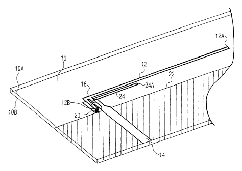
An embodiment of an inventive antenna device implemented on
a double-sided substrate 10 is shown in Fig. 1. It is to be
pointed out here that the substrate is illustrated in a
transparent manner in Fig. 1 for reasons of clarity. The
inventive antenna device illustrated in Fig. 1 principally
includes two integrated IFAs (inverted F antennas), one of
the antennas being formed on a top side 10a of the
McCarthy Tetrault LLP DOCS #664922 v. 2
CA 02523070 2005-10-20
- 8 -
substrate 10, the other one being formed on a bottom side
10b.
A first radiation electrode 12 comprising an open end 12a
and a short-circuited end 12b is formed on the main surface
l0a of the substrate 10 corresponding to the top side.
Additionally, a supply line 14 for galvanically feeding the
first radiation electrode 12 is provided on the main
surface 10a. The supply line 14 is connected to the first
radiation electrode 12 at a feeding point 16. With regard
to the structure of the metallizations provided on the main
surface 10a, i.e. the electrodes and lines provided there,
reference is made to Fig. 2a representing a top view of the
top side l0a of the relevant part of the substrate 10.
The short-circuited end 12b of the first radiation
electrode 12 is connected to a ground electrode 22 (in Fig.
1 illustrated in a hatched manner) formed on the main
surface lOb of the substrate 10 opposite the main surface
10a, via a through-connection 20. This opposite main
surface 10b (the back side in Fig. 1) is illustrated in
Fig. 2b as a "shine-through image" from above, wherein the
metallizations provided on the front side 10a are omitted
for reasons of clarity and the substrate is transparent. As
can best be seen in Fig. 2b, a second radiation electrode
24 comprising an open end 24a and a short-circuited end 24b
is formed on the main surface lOb. The short-circuited end
24b is connected to the ground electrode 22. Additionally,
a coupling conductor 26 comprising a first end connected to
the ground electrode 22 and a second end connected to:the:
second radiation electrode 24 at a coupling point 28 is
formed on the main surface lOb.
The ground , electrode is provided as a back side
metallization on the bottom side of the substrate and also
serves as a ground level for the microstrip line 14 and the
antennas. The galvanically fed, longer first radiation
electrode 12 is provided for the lower frequency band,
CA 02523070 2005-10-20
- 9 -
whereas the inductively fed, shorter antenna 24 is provided
for the upper frequency band.
The antenna shown in Fig. 1, in principle, consists of two
integrated IFAs, the first one of the two antennas for the
first frequency band being fed by the supply line 14 in the
form of a microstrip line. The second antenna for the
second frequency band comprising the second radiation
electrode 24 is inductively excited via a current loop. In
particular, in the embodiment illustrated, the supply line
14 and the portion of the first radiation electrode 12
between the short-circuited end 12b and the feeding point
16 form an exciter current loop generating a magnetic flux.
Additionally, the coupling line 26, the area of the second
radiation electrode 24 between the short-circuited end 24b
and the coupling point 28, and the ground electrode 22 form
an electric circuit. This electric circuit, in the
inventive antenna device, is arranged such that it is
infiltrated by the magnetic flux generated by the exciter
current loop such that a current is induced into this
current loop. The second radiation electrode 24 is fed by
this induced current.
In order to obtain the best possible magnetic coupling, in
the embodiment illustrated, the dimensions of the excited
current loop formed on the back side 10b roughly
corresponds to the dimensions of the exciter loop formed on
the front side 10a. The thickness of the substrate 10 may,
for example, be 0.5 mm so that the spacing of the current
loops on the top side and bottom side of the substrate,
respectively, is small (compared to the wave length at the
resonant frequency of the radiation electrode 24) such that
good magnetic coupling can be achieved.
In the embodiment shown, the radiation electrode 24 is thus
excited inductively by magnetic coupling, the intensity of
the coupling depending on the mutual inductivity between
the excitation conductor and the excited conductor. The
CA 02523070 2005-10-20
- 10 -
size and form of the exciter current loop and of the
excited current loop can be adjusted to obtain a desired
coupling. Additionally, the coupling depends on the mutual
distance of the loops.
It is to be pointed out here that the exciter current loop
and the excited current loop need not be closed current
loops formed on the substrate but may be formed as
conductor regions which, together with conductors not
formed on the substrate, form an alternating current
circuit or current loop. The exciter current loop need only
have one course to generate a sufficient magnetic field or
a sufficient magnetic flux such that a current sufficient
for a feeding current can be induced into the part of the
electric circuit of the second antenna element which is
arranged in the magnetic field or the magnetic flux.
Additionally, it is to be pointed out that the respective
current loops or electric circuits are formed in a way
suitable for enabling an alternating current flow such that_
capacitive couplings may be provided within these current
loops or electric circuits.
The feeding point 16 is selected to obtain impedance
matching between the microstrip line 14 and the radiation
electrode 12. The respective position for the feeding point
16 must be determined when designing the antenna, wherein
the antenna impedance may be diminished by shifting the
feeding point 16 to the left, whereas it can be increased
by shifting the feeding point 16 to the right, as is
indicated in Fig. 2a by an arrow 30. The antenna impedance
can thus be adjusted to the impedance of the galvanic
supply by correspondingly selecting the feeding point 16.
In the same way, matching between the antenna impedance of
the second radiation electrode 24 and the coupling line 26
can be obtained by suitably selecting the coupling point
28, as is shown in Fig. 2b by an arrow 32. It can be
achieved by this matching that the current induced may be
CA 02523070 2005-10-20
- 11 -
utilized optimally for feeding the second radiation
electrode.
Even though in the embodiment shown in Figs. 2a and 2b the
supply line 14 and the coupling line 26 are coupled to the
part of the respective radiation electrode parallel to the
edge of the ground electrode 22, each of these lines could
also be coupled to that part of the respective radiation
electrode perpendicular to the edge of the ground electrode
22, depending on how it is necessary to obtain impedance
matching.
The entire geometry of the inventive antenna device may be
reduced to obtain, for example, a minimization of the area
demand by, for example, forming the radiation electrodes or
at least the longer one thereof in a meandering shape.
The shape of the feed line 14a and the coupling line 26 and
the selection of the feeding point and the coupling point
26 may differ for obtaining impedance matching for the two
radiation electrodes to allow optimum matching for the two
individual antenna elements. The bend 14a in the supply
line 14 and the bend 26a in the coupling line 26 may, for
example, be provided in the embodiment shown in Figs. 1 and
2 to obtain impedance matching.
A schematic illustration for an embodiment of an inventive
multi-band antenna is shown in Fig. 3.
The multi-band antenna is implemented in a multi-layered
substrate 50 which in turn is shown in a transparent manner
for reasons of illustration and comprises a first layer 52
and a second layer 54. A first antenna element basically
corresponding to the antenna element formed on the top side
l0a of the substrate 10 comprising the first radiation
electrode 12, is formed on the top side of the first layer
52, wherein, in contrast to the embodiment shown in Fig. 1,
only the supply line 14 is connected to the part of the
CA 02523070 2005-10-20
- 12 -
radiation electrode 12 perpendicular to the edge of the
ground area 22 and thus has a corresponding portion 14b.
In analogy to the embodiment described above, the second
radiation electrode 24 is formed on the bottom side of the
first layer 52 (and on the top side of the second layer 54,
respectively). A third radiation electrode 56 having an
open end 56a and a short-circuited end 56b is formed on the
bottom side of the second layer 54. The short-circuited end
is connected to the ground electrode 22 via a through-
connection 58 provided in the second layer 54. In addition,
another through-connection 60 is provided in the second
layer 54, via which a first end of a coupling line 62 is
connected to the ground electrode 22. A second end of the
coupling line 62 is connected to the third radiation
electrode 56 at a coupling point 64.
The third antenna element comprising the radiation
electrode 56 thus has a setup comparable to the setup of
the second antenna element comprising the radiation
electrode 24.
In the embodiment shown in Fig. 3, the third radiation
electrode 56 is fed by at first inducing a current into the
electric circuit of the second antenna element and by
inducing a current into the electric circuit of the third
antenna element by the current induced into the electric
circuit of the second antenna element. This electric
circuit of the third antenna element is formed by a
conductor loop comprising the through-connection 60,:the
coupling line 62, the portion of the third radiation
electrode 56 arranged between the coupling point 64 and the
short-circuited end 56b, the through-connection 58 and the
ground electrode 22.
As can be seen in Fig. 3, the respective feeding points and
coupling points for the different antenna elements may be
CA 02523070 2005-10-20
- 13 -
arranged at different positions to obtain matching for the
respective different elements.
Alternatively to the embodiment shown in Fig. 3, the
galvanically fed antenna element could be arranged between
two inductively fed antenna elements so that no double
magnetic coupling would be required for feeding the third
antenna element.
In the embodiment shown in Fig. 3, instead of providing the
through-connection 60, the first end of the coupling line
64 could be connected to the short-circuited end of the
third radiation electrode 56 via a conductive track (not
shown) provided on the bottom side of the second layer 54
to implement the electric circuit of the third antenna
element. In such a case, only one respective through-
connection would be required in both the first layer 52 and
the second layer 54 of the multi-layered circuit board.
According to the invention, the several antenna elements
can be used for producing a dual-band or multi-band
antenna. Alternatively, respective additional antenna
elements may be used for expanding the bandwidth of an
individual frequency band by, for example, selecting the
resonant frequencies of two antenna elements to be adjacent
to each other.
Prototypes of inventive antenna devices have been simulated
by means of HFSS and then formed on an Ro4003 substrate
having an effective permittivity sr 3.38. An Ro4003
substrate is a high-frequency substrate by Rogers
Corporation and is made of a glass-reinforced cured
hydrocarbon/ceramics laminate. HFSS is an EM field
simulation software by Ansoft Corporation for calculating S
parameters and field configurations, which is based on the
finite elements method.
CA 02523070 2005-10-20
- 14 -
Fig. 4 purely schematically shows photographies of two
prototypes of this type in which the respective microstrip
supply line is fed by a coaxial line. To illustrate size
proportions, a 20 cent coin is also shown in Fig. 4. As can
be seen in Fig. 4, the left antenna has a somewhat narrower
radiation electrode, whereas the right antenna has a wider
radiation electrode.
Fig. 5a shows the characteristics obtained in input
reflection measurements of the left antenna of Fig. 4,
whereas Fig. 5b shows the characteristics obtained with the
right antenna of Fig. 4. As can be deduced from the graphs
of Figs. 5a and 5b, a change in bandwidth can be obtained
by varying the geometry.
Even though setups having only two or three radiation
electrodes have been described before, it is obvious that
the inventive concept may also be extended to more than
three radiation electrodes to obtain a corresponding multi-
band capability or broad-band capability. For this purpose,
a multi-layered substrate having more than two layers can
be used in a suitable way. In addition, the present
invention is not limited to the embodiments of antenna
devices described but rather also includes single-sided
printed antennas (where two or more radiation electrodes
are provided on one surface of the substrate) or wire
antenna assemblies.