Note: Descriptions are shown in the official language in which they were submitted.
CA 02523119 2005-10-21
WO 2004/098062 PCT/US2004/012577
COMBINED DIGITAL-TO-ANALOG CONVERTER AND SIGNAL FILTER
CROSS-REFERENCE TO RELATED APPLICATION
[0001] This application claims priority to U.S. Provisional application number
60/465,710,
filed April 24, 2003, entitled "Combined Digital-Analog Converter and Signal
Filtering." The entire content of this provisional application is incorporated
herein by
reference.
FIELD
[0002] This application relates to electronic filters, including low-pass
filters, and to digital-
to-analog converters. This application also relates to Ultra Wideband
communication
systems.
BACKGROUND
[0003] An electronic filter is a circuit that passes signals having certain
frequencies and
blocks signals having other frequencies. A filter that only passes signals
below a certain
frequency is commonly referred to as a low-pass filter; a filter that only
passes signals
above a certain frequency is commonly referred to as a high-pass filter; a
filter that only
passes signals within a range of frequencies is commonly referred to as a band
pass
filter; and a filter that only passes signals outside of a range of
frequencies is commonly
referred to as a notch filter.
[0004] Filters are traditionally designed to operate upon either analog or
digital signals.
[0005] An analog filter typically processes a continuously-varying signal.
Analog filters
typically include resistors, capacitors and, in some instances, inductors. The
function
that is provided by an analog filter is typically determined by the number and
value of
the components that are selected and by the manner in which they are
interconnected.
[0006] A digital filter typically processes a signal that alternates between a
number of
discrete levels, such as between two or three levels. Digital filters
typically include
serially-connected digital delay circuits, digital weighting (multipliers)
circuits, and
digital summers. The function that is provided by a digital filter is
typically determined
by the number of digital delay circuits, the magnitude of each delay, and the
weighting
of each weighting circuit.
CA 02523119 2005-10-21
WO 2004/098062 PCT/US2004/012577
2
[0007] Digital and analog filters are used in a broad variety of applications.
A low-pass
filter, for example, is often used in a transmitter to ensure that the
transmitter does not
transmit signals above the frequency authorized for communication by the FCC.
[0008] Some transmitters receive the information that is to be transmitted in
a digital
format. In these systems, the digital information signal is often converted to
an analog
signal by a digital-to-analog converter before it is transmitted.
[0009] In these digital information systems, the needed low-pass filter can be
placed either
before or after the digital-to-analog converter. If the low-pass filter is
placed before the
digital-to-analog converter, as shown in Fm. 1(a), the low-pass filter is
typically a
digital filter. If the low-pass filter is placed after the digital-to-analog
converter, as
shown in Fm. 1 (b), the low-pass filter is typically an analog filter.
[0010] New Ultra Wideband technology may enable wireless communication devices
to
simultaneously communicate wirelessly at an extremely low power level (e.g.,
10
nW/MHz) within an extremely wideband of several GHz and at speeds ranging from
1
MBps to 1 GBps.
[0011] However, the allowable bandwidth is not unlimited and thus may
therefore still need
to be controlled. To accomplish this, a low-pass filter may be used. The low-
pass filter
may need an extremely wide bandwidth to be able to faithfully process signals
at an
extremely low power level, but sharply cut off signals that are above the
cutoff.
[0012] One approach is to convert the digital information signal to an analog
signal and to
then deliver the analog signal through an analog low-pass filter, as shown in
Fig 1 (b).
Unfortunately, the analog filter may not be able to faithfully pass signals
within an ultra
wide bandwidth, while at the same time sharply cutting off signals above the
cut off. To
the contrary, an analog low-pass filter that has the required bandwidth and
sharply cuts
off signals above the cut off may distort the signals that are passed both in
amplitude
and by shifting their phase in an amount that varies as a fimction of their
frequency.
Analog low-pass filter designs that approach the necessary criteria may also
be quite
sensitive to variations in the value of their components, possibly requiring
expensive
components whose tolerances are closely regulated and not subject to
significant
changes due to varying environments. The necessary low-pass criteria may also
require
designs that are complex, expensive and hard to implement with analog
circuitry.
CA 02523119 2005-10-21
WO 2004/098062 PCT/US2004/012577
[0013] As indicated above and as shown in FIG. 1 (a), the low-pass filter in a
transmitter can
instead be inserted before the digital-to-analog converter. In this case, the
low-pass filter
may need to be a digital filter. If this configuration is used in connection
with an Ultra
Wideband transmitter, however, the necessary digital-to-analog converter may
need to
operate at an extremely high frequency and to simultaneously process a large
number of
bits to obtain the needed filtering resolution. This may increase the size,
power and
speed requirements of the digital-to-analog converter, as well as its cost.
Indeed, there
may not currently even be a practical digital-to-analog converter that can
meet all of the
necessary requirements for the new Ultra Wideband wireless communication
devices.
SUMMARY
[0014] An electronic circuit for processing a digital signal may include a
plurality of digital
delay circuits, each configured to produce a delayed replica of the digital
signal; a
plurality of digital-to-analog converters, each configured to convert the
digital signal or
the delayed replica from one of the delay circuits into an analog signal; a
plurality of
analog gain circuits, each configured to adjust the analog signal from one of
the digital-
to-analog converters by a gain factor and each having an output; and an analog
summer
configured to sum the outputs of the analog gain circuits.
[0015] An electronic filter may include an analog summer having a plurality of
inputs; a
plurality of analog gain circuits, each having an output coupled to one of the
inputs of
the analog signal summer and an input; a plurality of digital-to-analog
converters, each
having an output coupled to the input of one of the analog gain circuits and
an input;
and a plurality of serially-coupled digital delay circuits, each having an
output coupled
to the input of one of the plurality of digital-to-analog converters.
[0016] A method may include creating a set of digital replicas of a digital
signal, each of
the digital replicas being substantially the same as the digital signal, but
delayed in time
from the digital signal by an amount different than the delays of the other
digital
replicas; converting the digital signal and each of the delayed digital
replicas of the
digital signal into an analog signal; applying a gain factor to each of the
analog signals;
and summing the weighted analog signals.
[0017] An electronic circuit may include means for creating a set of digital
replicas of a
digital signal, each of the digital replicas being substantially the same as
the digital
signal, but delayed in time from the digital signal by an amount different
than the delays
CA 02523119 2005-10-21
WO 2004/098062 PCT/US2004/012577
4
of the other digital replicas; means for converting the digital signal and
each of the
delayed digital replicas of the digital signal into an analog signal; means
for applying a
gain factor to each of the analog signals; and means for summing the weighted
analog
signals.
[0018] Other embodiments will become readily apparent to those skilled in the
art from the
following detailed description, wherein only embodiments are shown and
described.
The details are also capable of modification in various other respects, all
without
departing from the spirit and scope of what is disclosed. The drawings and
detailed
description are to be regarded as illustrative in nature and not as
restrictive.
BRIEF DESCRIPTION OF DRAWINGS
[0019] Aspects of the present application are illustrated by way of example,
and not by way
of limitation, in the accompanying drawings, wherein:
[0020] FIGS 1 (a) and (b) are block diagrams of prior art digital-to-analog
converters that
include a low pass filter.
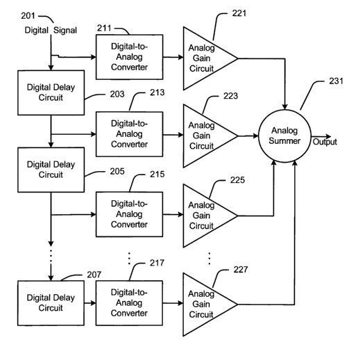
[0021] FIG. 2 is a block diagram of a combined digital-to-analog converter and
signal filter.
[0022] FIG. 3 is a flow diagram of a combined digital-to-analog converter and
signal filter.
(0023] FIG. 4 is a block diagram of a transmitter using a low-pass digital-to-
analog
converter.
[0024] FIG. 5 is a block diagram of a transceiver, such as used in a wireless
communication
device, using a low-pass digital-to-analog converter.
DETAILED DESCRIPTION
[0025] The detailed description set forth below in connection with the
appended drawings
is exemplary and does not represent the only embodiments that can be
practiced. The
term "exemplary" means "serving as an example, instance, or illustration," and
should
not necessarily be construed as preferred or advantageous over other
embodiments. The
detailed description includes specific details for the purpose of providing a
thorough
understanding of what is disclosed. In some instances, well-known structures
and
devices are shown in block diagram form in order to most clearly present the
concepts.
However, it will be apparent to those skilled in the art that these concepts
may be
practiced without these specific details.
CA 02523119 2005-10-21
WO 2004/098062 PCT/US2004/012577
[0026] FIG. 2 is a block diagram of a combined digital-to-analog converter and
signal filter.
[0027] As shown in FIG. 2, a digital signal 201 may be delivered into a series
of digital
delay circuits, such as digital delay circuits 203, 205 and 207.
[0028] Although the digital delay circuits are shown in FIG. 2 as being
coupled in a series,
they could, instead, be coupled to the digital signal 201 in parallel, in a
mixture of series
or parallel, or in any other configuration.
[0029] Each digital delay circuit may be configured to create an replica of
the digital signal
201, but delayed by a pre-determined amount in time. Each delay circuit may
consist of
only a single delay element or a series of cascaded delay elements.
[0030] The original and each delayed replica of the digital signal 201 may be
delivered to
the input of a digital-to-analog converter, such as to the inputs of digital-
to-analog
converters 211, 213, 215 and 217 shown in FIG. 2. As is well known, a digital-
to-analog
converter is a circuit that converts a digital signal into its analog
equivalent.
[0031] The analog output of each digital-to-analog converter may be delivered
to the input
of an analog gain circuit, such as to the inputs of analog gain circuits 221,
223, 225 and
227. As is well known, an analog gain circuit is an electronic circuit that
produces an
output that is substantially the same as its input, except multiplied by a pre-
determined
gain factor.
[0032] The output of each analog gain circuit may be delivered to the input of
an analog
summer, such as to the inputs of an analog summer 231 shown in FrG. 2. As is
well
known, an analog summer is an electronic circuit that produces an output that
is
substantially equal to the sum of its analog inputs. This output may
optionally be
multiplied internally by a gain factor within the analog summer.
[0033] FIG. 3 is a flow diagram of a combined digital-to-analog converter and
signal filter.
It illustrates the process implemented by the circuit described above in
connection with
FIG. 2.
[0034] Specifically, the process may begin by passing the digital signal
through a set of
delay circuits, as reflected by a Pass Digital Signal Through Delay Circuits
step 301.
[0035] The original and each delayed digital signal may then be converted to
an analog
signal, as reflected by a Convert Each Digital Signal To Analog Signal step
303.
CA 02523119 2005-10-21
WO 2004/098062 PCT/US2004/012577
6
[0036] A gain factor may be applied to each analog signal, as reflected by an
Apply Gain
Factor To Each Analog Signal step 305. The weighted analog signals may then be
summed, as reflected by a Sum Weighted Analog Signals step 307.
[0037] The number of the digital delay circuits that are utilized, as well as
the magnitude of
each delay and the gain factor of each analog gain circuit, may vary widely.
These
criteria may be selected such that the circuit in FIG. 2 implements a
filtering function.
The exact filtering function that is implemented may similarly be governed by
the
specific selections that are made.
[0038] As will be apparent to those skilled in the art, the circuitry
configuration shown in
Fm. 2 is similar to the configuration of a traditional digital filter.
However, a traditional
digital filter usually utilizes a digital gain circuit in place of the digital-
to-analog
converter and the analog gain circuit shown in FIG. 2 (e.g., the digital-to-
analog
converter 211 and the analog gain circuit 221).
[0039] Notwithstanding this difference, the considerations that go into
selecting the number
of digital delay circuits and the magnitude of each delay and gain factor in a
digital filter
may also be applied to the corresponding components shown in Fm. 2.
[0040] Using this knowledge in the art of digital filter design, the number of
digital delay
circuits and the magnitude of each delay and gain factor in FIG. 2 may be
selected to
implement almost any filter design, such as a low-pass filter, high-pass
filter, band pass
filter or notch filter. Further, the exact specification of the filter
(including the number
and placement of the zeros) can similarly be controlled by applying the
knowledge that
has been generated in connection with digital filter design.
[0041] The number of bits in each word of the digital signal 201 may also vary
widely. In
one example, the digital signal 201 may consist of only a single-bit digital
word. In this
case, the digital delay circuits, such as the digital delay circuits 203, 205
and 207, and
the digital-to-analog converters, such as the digital-to-analog converters
211, 213, 215
and 217, may be configured to process only a single bit word.
[0042] The ratio of the number of digital delay circuits to the number of
digital-to-analog
converters (and associated analog gain circuits) may also vary. In the example
shown in
FIG. 2, the number of digital-to-analog converters (and associated analog gain
circuits)
is equal to the number of digital delay circuits, plus one.
CA 02523119 2005-10-21
WO 2004/098062 PCT/US2004/012577
7
[0043] The combined digital-to-analog converter and signal filter that has
thus-far been
described may be used in a broad variety of applications.
[0044] FIG. 4 is a block diagram of a transmitter using a low-pass digital-to-
analog
converter. As shown in FIG. 4, a digital signal source 401 may be used to
deliver the
information signal that is to be transmitted in a digital format. This
information signal
could be representative of a voice, music, video, data or any other type of
information or
a combination of these types.
[0045] To ensure that the digital signal provided by the digital signal source
401 does not
go above a needed cutoff, the digital signal may be delivered to a low-pass
digital-to-
analog converter. The low-pass digital-to-analog converter may be a combined
digital-
to-analog converter and signal filter, such as the circuit illustrated in FIG.
2 and
implementing the process illustrated in FIG. 3, all as described above in more
detail. In
this example, the number of digital delay circuits and the magnitude of each
delay and
associated gain factor may be selected in accordance with standard digital
filter design
techniques to implement a low-pass digital-to-analog converter 403 that meets
the
necessary low-pass specification.
[0046] The output of the low-pass digital-to-analog converter 403 may be
delivered to a
modulator 405 that mixes the output of the low-pass digital-to-analog
converter 403
with a Garner signal generated by a local oscillator 407. The output of the
modulator
405 may be delivered to an amplifier 409 to increase the strength of the
modulated
carrier. The output of the amplifier 409 may be delivered to an antenna 411 to
radiate
the amplified and modulated signal. In very low power configurations, the
amplifier 409
may not be present or, if present, may not be used.
[0047] FIG. 5 is a block diagram of a transceiver that may be used in any
wireless
communication device and that uses a low-pass digital-to-analog converter. As
shown in
FIG. 5, the transceiver may include a transmitter with low-pass digital-to-
analog
converter 501. This may be of the type described above in connection with FrG.
4. It
may also include a receiver 503 and an antenna 505 that is switched between
the
transmitter 501 and the receiver 503 with a switch 507. The switch 507 may be
mechanically operated, voice-actuated, or operated by other means.
[0048] Although now having been discussed in the context of a transmitter
(FIG. 4) and a
transceiver (FIG. 5), the combined digital-to-analog converter and signal
filter shown in
CA 02523119 2005-10-21
WO 2004/098062 PCT/US2004/012577
8
FIG. 2 and the related process shown in FIG. 3 may be used in a broad variety
of
applications. For example, the combined digital-to-analog converter and signal
filter
may be used in connection with applications that require a finite impulse
response (FIR)
digital filter, as well as an infinite impulse response (IIR) digital filter.
In the case of an
IIR filter, circuitry may need to be added in the feedback path to match the
analog
output of the combined digital-to-analog converter and signal filter to the
digital input.
[0049] The combined digital-to-analog converter and signal filter may support
pre-
correction functionality for antenna and other analog or digitally-induced
amplitude
and/or phase distortions.
[0050] The circuitry used in the combined digital-to-analog converter and
signal filter may
be incorporated into a single, mixed-mode integrated circuit chip.
[0051] Those of skill in the art will understand that information and signals
may be
represented using any of a variety of different technologies and techniques.
For
example, data, instructions, commands, information, signals, bits, symbols,
and chips
that may be referenced above may be represented by voltages, currents,
electromagnetic
waves, magnetic fields or particles, optical fields or particles, or any
combination
thereof.
[0052] Those of skill will further appreciate that the various illustrative
logical blocks,
modules, circuits, and algorithm steps described in connection with the
embodiments
disclosed herein may be implemented as electronic hardware, computer software,
or
combinations of both. To clearly illustrate this interchangeability of
hardware and
software, various illustrative components, blocks, modules, circuits, and
steps have been
described above generally in terms of their functionality. Whether such
functionality is
implemented as hardware or software depends upon the particular application
and
design constraints imposed on the overall system. Skilled artisans may
implement the
described functionality in varying ways for each particular application, but
such
[0053] implementation decisions should not be interpreted as causing a
departure from the
scope of what is disclosed.
[0054] The various illustrative logical blocks, modules, and circuits
described in connection
with the embodiments disclosed herein may be implemented or performed with a
general purpose processor, a digital signal processor (DSP), an application
specific
CA 02523119 2005-10-21
WO 2004/098062 PCT/US2004/012577
9
integrated circuit (ASIC), a field programmable gate array (FPGA) or other
programmable logic device, discrete gate or transistor logic, discrete
hardware
components, or any combination thereof designed to perform the fimctions
described
herein. A general purpose processor may be a microprocessor, but in the
alternative, the
processor may be any conventional processor, controller, microcontroller, or
state
machine. A processor may also be implemented as a combination of computing
devices,
e.g., a combination of a DSP and a microprocessor, a plurality of
microprocessors, one
or more microprocessors in conjunction with a DSP core, or any other such
configuration.
[0055] The steps of a method or algorithm described in connection with the
embodiments
disclosed herein may be embodied directly in hardware, in a software module
executed
by a processor, or in a combination of the two. A software module may reside
in RAM
memory, flash memory, ROM memory, EPROM memory, EEPROM memory,
registers, hard disk, a removable disk, a CD-ROM, or any other form of storage
medium
known in the art. An exemplary storage medium is coupled to the processor such
the
processor can read information from, and write information to, the storage
medium. In
the alternative, the storage medium may be integral to the processor. The
processor and
the storage medium may reside in an ASIC. In the alternative, the processor
and the
storage medium may reside as discrete components in a user terminal.
[0056] The previous description of the disclosed embodiments is provided to
enable any
person skilled in the art to make or use the concepts that are disclosed.
Various
modifications to these embodiments will be readily apparent to those skilled
in the art,
and the generic principles defined herein may be applied to other embodiments
without
departing from the spirit or scope of what is disclosed. Thus, the present
application is
not intended to be limited to the embodiments shown herein but is to be
accorded the
widest scope consistent with the principles and novel features disclosed
herein.