Note: Descriptions are shown in the official language in which they were submitted.
CA 02524214 2005-10-28
WO 2004/097987 PCT/FI2004/000260
1
Antenna arrangement and base transceiver station
Field
The invention relates to an antenna arrangement in a base trans-
ceiver station of a telecommunication system and to a base transceiver station
s of a cellular telecommunication system.
Background
It is well known that the location of antenna elements of a base
transceiver station plays a crucial role in the quality of transmitted and
received
radio signals, and therefore has a strong impact on the capacity of the base
transceiver station and the entire cellular telecommunication system.
It is customary to locate the antenna elements such that the cover-
age of the cell of the base transceiver station is as good as possible in the
cell
area. A good coverage may be obtained, for example, by locating the antenna
elements in elevated sites by using masts dedicated for wireless communica-
15 tion or other high constructions, such as buildings, while other parts,
such as
radio frequency parts and base band parts, of the base transceiver station are
located on the ground far from the antenna elements.
A physical distance between the antenna elements and the other
parts of the base transceiver station involves a power distribution system for
2o relaying electric signals between the antenna elements and the other parts
of
the base station. The power distribution system may comprise branches to a
plurality of antenna elements if antenna groups are utilized. The power distri-
bution system may comprise cables, such as co-axial cables, between the
transceiver of the base station and the antenna elements and possibly mast
25 amplifiers used as pre-amplifiers. The multi-antenna techniques usually
require
accurate relative signal characteristics, such as phase and amplitude, between
the antenna signals of different antenna elements so that the desired
radiation
pattern provided by an antenna group can be achieved.
The electric characteristics of the power distribution system give rise
so to electric disturbance, such as loss and retardation, in the signals
transmitted
between the antenna elements and other parts of the base transceiver station.
Especially, if multi-antenna techniques are utilized, the power distribution
sys
tem may comprise branches with different electric characteristics, thus
distort
ing the relative signal characteristics of the antenna signals, and reducing
the
35 quality of transmission and reception of the base transceiver station. The
re-
CA 02524214 2005-10-28
WO 2004/097987 PCT/FI2004/000260
2
duction in the quality of the transmission and reception further leads to
lower in
capacity of the base transceiver station and the entire cellular telecommunica-
tion system.
Brief description of the invention
An object of the invention is to provide an improved antenna ar-
rangement and a base transceiver station for reducing problems associated
with the power distribution system between a base station and antenna ele-
ments of the base transceiver station.
According to a first aspect of the invention, there is provided an an-
tenna arrangement of a base transceiver station of a cellular telecommunica-
tion system, the antenna arrangement comprising: at least one active antenna
for performing conversion between a low-frequency digital signal and a radio
frequency electromagnetic field, the at least one active antenna comprising an
antenna element for performing conversion between a radio frequency signal
and the radio frequency electromagnetic field, and a transceiver coupled and
integrated at feast partially with the antenna element for performing
conversion
between the low-frequency digital signal and the radio frequency signal.
According to a second aspect of the invention, there is provided a
base transceiver station of a cellular telecommunication system, the base
2o transceiver station comprising: a local unit connected to a network of the
cellu
lar telecommunication system for digital signal processing; and at least one
active antenna connected to the local unit, for performing conversion between
a low-frequency digital signal and a radio frequency electromagnetic field,
the
at least one active antenna comprising an antenna element for performing
conversion between a radio frequency signal and the radio frequency electro-
magnetic field, and a transceiver coupled and integrated at least partially
with
the antenna element, for performing conversion between the low-frequency
digital signal and the radio frequency signal.
The antenna arrangement and the base transceiver station accord
3o ing to the invention provide several advantages. The digital form of low
frequency digital signal transmitted between the active and the base band
parts of the base station together with the integrated structure of the trans
ceiver and the antenna element enable a low-disturbance power distribution
system to be located relatively far from the base band parts of the base trans
ceiver station.
CA 02524214 2005-10-28
WO 2004/097987 PCT/FI2004/000260
3
List of the drawings
In the following, the invention will be described in greater detail with
reference to preferred embodiments and the accompanying drawings, in which
Figure 1 shows an example of the structure of a cellular communi-
s cation system;
Figure 2 shows an example of the structure of a base transceiver
station according to the invention,
Figure 3 shows a first example of the structure of an active antenna
according to the invention,
Figure 4 shows an example of the structure of a radio modem ac-
cording to the invention,
Figure 5A shows a second example of the structure of an active an-
tenna according to the invention, and
Figure 5B shows a third example of the structure of an active an-
15 tenna according to the invention, and
Figure 6 shows an example of the structure of an antenna arrange-
ment according to the invention.
Description of embodiments
Figure 1 illustrates an example of a simplified structure of a tele-
2o communication system to which the invention may be applied.
The cellular telecommunications system is based on, for example, a
GSM (Global System for Mobile Communications) radio access technology or
WCDMA (Wideband Code Division Multiple Access) technology. The structure
and function of cellular telecommunications systems are known to a person
25 skilled in the art, and only network elements relevant to the invention
will be
described.
In the example shown in Figure 1, the network elements are pre-
sented in terms of GSM terminology using circuit-switched network elements
without restricting applications of the invention to the GSM system.
so The cellular telecommunication system comprises a mobile switch-
ing centre (MSC) 104 enabling circuit-switched signalling in the cellular tele-
communications system.
The cellular telecommunications system may also comprise a gate
way mobile services switching centre 102 (GMSC). The GMSC attends to the
35 circuit-switched connections between the core network comprising the MSC
CA 02524214 2005-10-28
WO 2004/097987 PCT/FI2004/000260
4
and the GMSC, and external networks (EXT) 100, such as a public land mobile
network (PLMN) or a public switched telephone network (PSTN).
The MSC 104 controls a radio access network comprising at least
one base station controller (BSC) 106 and a base transceiver station (BTS)
s 108, 118 controlled by the BSC 106. The base station controller 106 repre
sents in general network elements, such as a radio network controller (RNC),
which act as an interface between the core network and the radio access net-
work. The base transceiver station 108, 118 represents network elements,
such as node B, which implements the radio interface in the cellular telecom-
munication system. The invention is not, however, restricted in the presented
structure of the cellular telecommunication system, but can be applied to any
cellular telecommunication, such as a CDMA2000 system.
The telecommunication system further comprises user equipment
110, 120, 128 for providing a user with access to the cellular telecommunica
15 tion system. The user equipment 110, 120, 128 may comprise conventional
components, including wireless modems, processors with software, memory, a
user interface, and a display. The structure and functions of the user equip-
ment 110, 120, 128 are known to a person skilled in the art.
Figure 1 shows the structure of the coverage area of the exemplified
2o cellular telecommunication system and implementation thereof. The base
transceiver station 108 provides the user equipment 110 with a macro-cell 116,
whose coverage area may range from hundreds of meters to several kilome
tres. In order to obtain such a large coverage area, the antenna element 112
may be located in an elevated location, such as the top of a mast. The macro
2s cell 116 may also represent an adaptive cell, which can dynamically be di-
rected at the user equipment 110 according to the prevailing location and ca-
pacity requirement of the user equipment 110.
A smaller cell size may be employed in order to improve the cover
age area provided by the macro-cell 116 or to form high capacity sites. Exam
ao pies of such smaller cells include e.g. a micro-cell 124 and a pico-cell
130 are
shown. A base transceiver station 118 may provide several micro- and/or pico-
cells. The size of a micro-cell 124 may range from hundreds of meters to doz-
ens of meters while the size of a pico-cell 130 may range from meters to cen-
timetres.
35 The antenna element placement in the micro- and pico cell imple-
mentations may vary. Micro-cell antenna elements 122 may be located in
CA 02524214 2005-10-28
WO 2004/097987 PCT/FI2004/000260
buildings or a wall of a building while pico-cell antenna elements 126 are usu-
ally located in the proximity of the users in order to obtain direct
visibility.
The cell implementations utilize a base transceiver station structure
wherein the antenna element 112, 122, 126 is located far from the other parts
s of the base station 108, 118. Therefore, a connecting means 132 are required
between the antenna element 112 and the other parts of the base transceiver
station 108, 118.
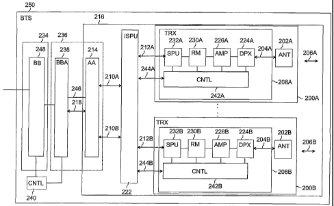
Figure 2 exemplifies embodiments of an antenna arrangement 216
according to the first aspect of the invention, and embodiments of a base
~o transceiver station 250 according to the second aspect of the invention.
The
base transceiver station 250 and the antenna arrangement 216 are capable of
transmitting and receiving radio signals. For the sake of simplicity, the
transmit-
ted signals and received signals are shown by using a single set of reference
numerals.
The antenna arrangement 216 comprises at least one active an-
tenna 200A, 2008. The active antenna 200A, 2008 comprises an antenna
element 202A, 2028, and a transceiver 208A, 2088 coupled and integrated at
least partially with the antenna element 202A, 2028.
In transmission, the antenna element 202A, 2028 receives a radio
2o frequency transmit signal 204A, 2048 from the transceiver 208A, 2088 and
converts the radio frequency transmit signal 204A, 2048 into a radio frequency
electromagnetic field 206A, 2068, which may as such compose a radiation
pattern or produce elementary components in an overall electromagnetic field
produced in superposition with other antenna elements. The electromagnetic
field 206A, 2068 enables a downlink connection between user equipment 110,
120, 130 and a base transceiver station 108, 118, 250.
In reception, the antenna element 202A, 2028 performs a spatial sampling of
an electromagnetic field 206A, 2068 produced by a radio signal source, such
as user equipment 110, 120, 130, thus converting a portion of the radio fre-
3o quency electromagnetic field 206A, 2068 into a radio frequency receive
signal
204A, 2048 to be fed into the transceiver 208A, 2088. In reception, the elec-
tromagnetic field 206A, 2068 enables an uplink connection between the user
equipment 110, 120, 130 and a base transceiver station 108, 118, 250. The
antenna element 202A, 2028 may be a patch antenna or a dipole, for exam-
ple. An oscillating frequency of the radio frequency electromagnetic field
206A,
2068 may range, for example, from 850 MHz corresponding to GSM 850 sys-
CA 02524214 2005-10-28
WO 2004/097987 PCT/FI2004/000260
6
tem frequency to 1900 MHz corresponding to GSM1900 system frequency.
The invention is not, however, restricted in the above frequencies but may be
applied to any radio frequency utilized in a cellular telecommunication
system.
In transmission, a low-frequency digital transmit signal 212A, 212B
is inputted into the transceiver 208A, 208B. The low-frequency digital
transmit
signal 212A, 212B is converted into a radio frequency transmit signal 204A,
204B by the transceiver 208A, 208B.
In reception, the transceiver 208A, 208B converts the receive radio
frequency receive signal 204A, 204B into a low-frequency digital output signal
~0 212A, 212B, and outputs the low-frequency digital output signal 212A, 212B.
In an embodiment, the low-frequency digital signal 212A, 212B
represents a signal similar to a base band signal used in base band parts in a
base transceiver station. The format of the low-frequency digital signal 212A,
212B may, however, differ from that used in conventional base band parts.
In an embodiment, the antenna arrangement comprises an antenna
adapter 214 connected to the at least one active antenna 200A, 200B for pro-
viding a digital link for the at least one active antenna 200A, 200B. The
digital
link is implemented by transmitting a digital link signal 218 between the an-
tenna adapter 214 and other parts of the base transceiver station. In transmis-
2o sion, the antenna adapter 214 receives a digital link signal 218 and
converts
the digital link signal 218 into the low-frequency digital transmit signal
212A,
212B to be inputted into the transceiver 208A, 208B.
In reception, the antenna adapter 214 receives the low-frequency
digital output signal 212A, 212B from the active antenna 200A, 200B and con-
es verts the low-frequency digital output signal 212A, 212B into the digital
link
signal 218.
A digital link provides several advantages over analogue links. The
bit form of the information enabled by the digital link, for example, enables
reli-
able and flexible information transfer, since losses in the digital link have
a
so small effect on the information content transferred by the digital link.
In an embodiment, the digital link signal 218 is implemented by us-
ing optical radiation such that the information carried by the digital link
signal
218 is coded digitally as intensity variation of the optical radiation.
In transmission, the antenna adapter 214 receives optical radiation
a5 carrying the digital link signal 218, detects the optical radiation with a
light de
tector, and converts the optical radiation into an electric form. The electric
form
CA 02524214 2005-10-28
WO 2004/097987 PCT/FI2004/000260
7
of the optical radiation may be amplified and filtered. The electric form of
the
optical radiation may be sampled, and the low-frequency digital transmit
signal
212A, 212B is formed based on sampling.
In reception, the antenna adapter 214 may modulate the optical ra-
diction such that the information content of the low-frequency digital output
signal 212A, 212B is transferred into the digital link signal 218. The optical
ra-
diation may be produced by using known techniques, such as light emitting
semiconductors.
The digital link signal 218 may be implemented by using optical
~o channels based on optical properties, such as polarization or an optical
wave-
length, of the optical radiation used in implementing the digital link signal
218.
The optical components and methods used in the implementation of the optical
channels are known to a person skilled in the art.
The optical form of the digital link signal 218, for example, enables
15 high information transfer capacity for the digital link signal 218.
In an embodiment, the digital link signal 218 has a predetermined
frame structure, wherein each frame and/or portion of a frame has frame-
specific information, such as payload data and control information.
Figure 3 shows an example of the structure of an active antenna
20 340 according to the invention. Antenna elements 300 and a transceiver 302
are shown.
A low-frequency digital signal 326A represents a transmission por-
tion of the low-frequency digital signal 212A, 2128 shown in Figure 2. A low-
frequency digital signal 326B represents a receive portion of the low-
frequency
25 digital signal 212A, 212B shown in Figure 2.
A radio frequency transmit signal 322A represents a transmit portion
of the radio frequency signal 204A, 204B. A radio frequency receive signal
322B represents a receive portion of the radio frequency signal 204A, 204B.
In an embodiment, the transceiver 208A, 208B, 302 comprises a ra
so dio modem (RM) 230A, 230B, 314 for performing frequency conversion be
tween the low-frequency digital signal 212A, 212B, 328A, 328B and the radio
frequency signal 204A, 204B, 322A, 322B. The radio modem 230A, 230B, 314
may perform the conversion between the low-frequency digital signal 212A,
212B, 328A, 328B and the radio frequency signal 204A, 204B, 322A, 322B in
35 one or more steps utilizing direct conversion or intermediate frequencies.
CA 02524214 2005-10-28
WO 2004/097987 PCT/FI2004/000260
8
Figure 4 shows an example of a structure of a radio modem 230A,
230B, 314 employing direct conversion.
The radio modem 230A, 230B, 314 may comprise an ana-
logue/digital converter unit 400 for performing conversion between a low-
s frequency digital signal 414A, 414B, 414C, 414D and a low-frequency electric
analogue signal 418A, 418B, 418C, 418D.
The radio modem 230A, 230B, 314 may further comprise a modula-
tor unit 408 for performing frequency conversion between the low-frequency
electric analogue signal 418A, 418B, 418C, 418D and a radio frequency signal
416A, 416B.
In transmission, the radio modem 230A, 230B, 314 receives the
low-frequency digital transmit signal 328A, 414A, 414B into an up-converter
410A and up-converts the low-frequency digital transmit signal 328A, 414A,
414B into the radio frequency transmit signal 322A, 416A. The low-frequency
~5 digital transmit signal 322A, 416A may be divided into a first digital
transmit
component 414A and a second digital transmit component 414B. The two digi-
tal transmit components 414A and 414B may contain signal characteristics,
such as power and phase characteristics, of the radio frequency transmit sig-
nal 416A. The frequency of the up-converter 41 OA is controlled by a local
oscil-
lator 420A.
The analogue/digital converter unit may 400 comprise a digital-to-
analogue converter 402A (ADC) for converting the low-frequency digital trans-
mit signal 414A, 414B into the low-frequency electric analogue signal 418A,
418B. In an embodiment, the digital-to-analogue converter 402A includes
separate converters for the first digital transmit component 414A and the sec-
ond digital transmit component 414B, thus producing a first analogue transmit
component 418A and a second analogue transmit component 418B.
In reception, the radio modem 230A, 230B, 314 receives the radio
frequency receive signal 322B, 416B into a down-converter 410B of the modu
lator unit 408, and down-converts the radio frequency receive signal 322B,
416B into a low-frequency analogue electric receive signal 418C, 418D. Next,
the low-frequency analogue electric receive signal 418C, 418D is fed into an
analogue-to-digital converter 402B of the analogue/digital converter unit 400,
which converts the low-frequency analogue electric receive signal 418C, 418D
s5 into the low-frequency digital signal 228B, 414C, 414D. The frequency of
the
up-converter 41 OB is controlled by a local oscillator 420B.
CA 02524214 2005-10-28
WO 2004/097987 PCT/FI2004/000260
9
The first analogue receive component 418C and the second ana-
logue receive component 418D are fed into analogue-to-digital converters
402B of the analogue/digital converter unit 400, which samples the two ana-
logue receive components 418C, 418D, thus producing the low-frequency digi-
tal receive signals 226B 414C, 414D to be fed into the antenna adapter 214.
In an embodiment, the radio modem 230A, 230B, 314 is imple-
mented using a printed board shared with the antenna unit 202A, 202B, 300.
The radio modem 230A, 230B, 314 may further be implemented using an inte-
grated circuit placed on the printed board. This implementation enables an in-
tegrated structure of the active antenna 200A, 200B, 340, which may employ
teachings and electrical components in connection with user equipment im-
plementations.
In an embodiment, the transceiver 208A, 208B, 302 comprises a fil-
ter unit (DPX) 224A, 224B, 310 connected to the antenna element 200 for limit-
~5 ing the frequency spectrum of the radio frequency signal 204A, 204B, 322A,
322B. The filter unit 224A, 224B, 310 may include a transmit filter 334A with
a
transmit pass band corresponding to the carrier frequencies used in the
downlink direction. The filter unit 224A, 224B, 310 may further comprise a re-
ceive filter 334B with a receive pass band corresponding to the carrier fre-
2o quencies used in the uplink direction. The transmit filter 334A and the
receive
filter 334B may be chosen and/or tuned such that the filter unit 224A, 224B,
310 composes a diplexer for separating the downlink and uplink frequency
from each other.
In an embodiment, the filter unit 224A, 224B, 310 is connected to
25 the radio modem 230A, 230B, 314. This implementation is preferable when a
low power level is sufficient for transmission and possibly reception, for
exam-
ple, in pico-cell 130 formation.
In an embodiment, the filter unit 224A, 224B, 310 is implemented on
a printed board shared with the antenna element 202A, 202B, 300, thus pro-
3o viding an integrated structure for the active antenna 200A, 200B, 340. The
in-
tegrated structure enables utilizing filter techniques and components conven-
tionally used in connection with user equipment implementations.
In an embodiment, the transceiver 208A, 208B, 302 comprises an
amplifier unit (AMP) 226A, 226B, 312 for amplifying the radio frequency signal
s5 204A, 204B, 322A, 322B. In an embodiment, the amplifier unit 226A, 226B,
312 is connected to the radio modem 230A, 230B, 314.
CA 02524214 2005-10-28
WO 2004/097987 PCT/FI2004/000260
In an embodiment, the amplifier unit 226A, 226B, 312 comprises a
transmit amplifier 316A, such as a linear power amplifier, for amplifying the
transmit radio frequency signal 322A to be directed at the antenna element
300. The transmit amplifier 316A enables amplifying the radio frequency
5 transmit signal 322A such that the strength of the electromagnetic field is
at a
desired level.
In an embodiment, the amplifier unit 226A, 226B, 312 comprises a
receive amplifier 316B, such as a low noise amplifier, for amplifying the
receive
radio frequency signal 322B. The receive amplifier 316B enables the receive
radio frequency signal 322B to be amplified such that after amplification, the
power of the receive radio frequency signal 322B is at a level suitable for
other
parts of the transceiver 208A, 208B, 302, such as the radio modem 230A,
230B, 314.
In an embodiment, the amplifier unit 226A, 226B, 312 is imple-
~5 mented with an integrated circuit placed on a printed board in common with
the
antenna element 202A, 202B, 300, and possibly the radio modem 230A, 230B,
314, thus providing an integrated structure for the active antenna 200A, 200B,
340. The integrated structure enables amplifier techniques and electrical com
ponents, such as integrated amplifier circuits, to be utilized used in
connection
2o with user equipment implementations.
In an embodiment, the transceiver 208A, 208B, 302 comprises a
signal processing unit (SPU) 232A, 232B, 318 for processing the low-
frequency digital signal 212A, 212B, 326A, 326B.
In transmission, the signal processing unit 232A, 232B, 318 re-
25 ceives and performs processing on the low-frequency digital transmit signal
212A, 212B, 328B. The tasks the signal processing unit 232A, 232B, 318 per-
forms on the low-frequency digital transmit signal 226A include: digital
filtering,
signal characteristics adjustment, power amplifier linearization, implementing
signal shaping functions, digital pre-distortion. Some of the tasks may
require
so feedback information from the antenna signal path comprising components
between the signal processing unit 232A, 232B, 318 and the antenna element
202A, 202B, 300. Furthermore, the signal processing unit 232A, 232B, 318
may deal with tasks associated with operation and maintenance, such as
alarms and control. The digital signal processor 232A, 232B, 318 outputs a
35 processed low-frequency digital signal 328A, which is received, for
example,
by the radio modem 314.
CA 02524214 2005-10-28
WO 2004/097987 PCT/FI2004/000260
11
In reception, the digital signal processing unit 232A, 232B, 318 re-
ceives a low-frequency digital receive signal 228B produced by, for example,
the radio modem 314, and processes the low-frequency digital receive signal
228B. The tasks the digital signal processing unit 318 performs on the low-
frequency digital receive signal 328B include: digital filtering, preliminary
phase
adjustment, operation and maintenance.
In an embodiment, the digital signal processing unit 232A, 232B,
318 is implemented using a printed board in common with the antenna element
202A, 202B, 300 and possibly the radio modem 230A, 230B, 314 the amplifier
unit 226A, 226B, 312, and the filter unit 224A, 224B, 310. The signal process-
ing unit 232A, 232B, 318 may include a digital signal processor, memory
means and software suitable for the tasks listed. The signal processing unit
218 may be implemented using a digital computer chip placed on the printed
circuit, thus providing an integrated structure for the active antenna 200A,
15 200B, 340. In an embodiment, the transceiver 208A, 208B, 302 supports a
multi-carrier operation of a cellular telecommunication system. The multi-
carrier operation includes capability of tuning the transceiver 208A, 208B,
302
over a wide range of radio frequencies while the frequency of the low-
frequency digital signal 212A, 212B, 326A, 326B, 328A, 328B is fixed.
2o In an embodiment, the active antenna 200A, 200B, 340 comprises a
control unit 242A, 242B, 332, 412 connected to the transceiver 208A, 208B,
302 for controlling the active antenna 200A, 200B, 340.
In an embodiment, the control unit 242A, 242B, 332 is connected to
the antenna adapter 214 in order to transmit control information 244A, 244B,
25 326C between the control unit 242A, 242B, 332 and the antenna adapter 214.
The control information may be associated with the following: beam forming,
linearization of the radio frequency signals, pre-distorting of the radio fre-
quency signals, time reference, power control, phase control, signal
splitting,
information on the status of a remote antenna 238.
3o The control unit 242A, 242B, 332 may be implemented with a digital
computer with software and possibly means for measuring electric signals from
the transceiver 208A, 208B, 302.
In an embodiment of the invention, the digital link signal 218 con-
tains a control frame which includes control information for controlling the
ac-
35 tive antenna 200A, 200B, 340.
CA 02524214 2005-10-28
WO 2004/097987 PCT/FI2004/000260
12
In an embodiment of the invention, the control unit 332 is configured
to collect feedback information 336, 338 from the transceiver 302 and perform
control tasks accordingly. The feedback information may 336, 338 be obtained
by measuring electric signals from the transmit branch and/or receive branch
of the transceiver 302. The control tasks requiring feedback information in-
clude, for example, digital pre-distortion and phase adjustment.
The control unit 242A, 242B may be connected to the antenna
adapter 214 such that a dedicated digital control signal 326A, 326B is relayed
between the transceiver 208A, 208B, 302 and the antenna adapter 214. It is
~o also possible to multiplex the control information in the low-frequency
digital
signal 212A, 212B, 326A, 326B and extract the control information from the
low-frequency digital signal 212A, 212B, 326A, 326B digitally.
In an embodiment, the antenna arrangement 216 comprises an in
terface signal processing unit (ISPU) 222 connected to at least one active an
tenna 200A, 200B and the antenna adapter 214 for processing signals 212A,
212B, 210A, 210B transmitted between the active antenna 200A, 200B and
the antenna adapter 214. The interface signal processing unit 222 may sepa-
rate different frames in the digital link signal 218 and possibly code the
frames
into suitable format for the transceiver 208A, 208B. The separation includes,
2o for example, separating the payload data and control data from the bit
stream,
and routing the different types of data into suitable connectors of the trans-
ceiver 208A, 2088. Furthermore, the interface signal processing unit 222 may
combine data of different optical channels and/or direct the data to different
optical channels. The combining includes forming the bit stream from the low-
frequency digital receive signal 212A, 212B, 326B and possibly from control
signal signals such that the digital link signal 218 to be transmitted from
the
antenna adapter 214 has a predetermined frame structure.
Furthermore, the tasks the interface signal processing unit 222 per-
forms in transmission include:
- calculating or watching, from a look up table, phase and power set-
ting values for each antenna element 202A, 202B, 300 according to a desired
radiation pattern
- setting the power level for each antenna element 202A, 202B, 300
directly or distributing power weight information to each signal processing
unit
232A, 232B, 318
CA 02524214 2005-10-28
WO 2004/097987 PCT/FI2004/000260
13
-distributing phase setting data to each signal processing unit 232A,
232B, 318
- distributing operation and maintenance commands to active an-
tennas 200A, 200B, 340.
The tasks the interface signal processing unit 222 performs in re-
ception include:
-reducing n data streams coming from the individual active antennas
200A, 200B, 300 into one common data stream
-phase tracking
~o -performing noise and interference cancellation using e.g. correla-
tion or other suitable algorithms on the several data streams coming from the
individual active antennas 200A, 200B, 340
-operation and maintenance command distribution.
The interference signal processing unit 222 may comprise a digital
~5 signal processor with software. In a broad interpretation, the interface
signal
processing unit 222 may comprise an application specific integrated circuit
(ASIC) designed for the dedicated tasks of the interface signal processing
unit
222. Therefore, reducing the n data streams into one common data stream, for
example, may not require actual signal processing power but just adjusting the
2o phases of incoming data streams so that they emulate the desired phase com-
ponent of the illumination function provided by the antenna arrangement 216
and setting the antenna weights for summing so that also the power compo-
nent of the mentioned illumination function is correct. In an embodiment, the
interface signal processing unit 222 performs tasks aimed at increasing the
25 sensitivity of reception. This role of the interface signal processing unit
222
reduces the need for costly hardware of the active antennas 200A, 200B, 340.
In an embodiment, the digital link signal 218 includes signal characteristics,
such as power information and phase information, of the radio frequency signal
222A, 222B.
so In an embodiment, at least one active antenna 200A, 200B is con-
figured to support at least two radio systems, such as GSM900, GSM850,
GSM1800, GSM1900, WCDMA, and CDMA2000. The transceiver 208A, 208B,
302 may include parallel radio system-specific components, such as radio mo-
dems 230A, 230B, 312 and software. However, some components, such as
35 antenna element 202A, 202B, 300, may be shared.
CA 02524214 2005-10-28
WO 2004/097987 PCT/FI2004/000260
14
Figures 5A and 5B exemplify the structure of an active antenna
200A, 200B, 340, showing a transceiver 502 and an antenna element 510.
In an embodiment of the invention, an antenna element 510 and a
transceiver 502 are integrated into a common electromechanical structure 504.
s The electromechanical structure 504 may be a printed board or an integrated
. circuit. The electromechanical structure 504 may comprise internal wiring
for
interconnecting the components, such as integrated circuits and antenna ele-
ments 510.
In an embodiment of the invention, the antenna element 510 and
the transceiver 502 are situated in opposite sides of the electromechanical
structure 504. This configuration enables a compact structure for the active
antenna 200A, 200B, 340.
In an embodiment, the electromechanical structure 504 comprises a
parallel bus 506 connected to the transceiver 502 for interconnecting the elec-
~5 tromechanical structure 504 with an external parallel bus 508. The parallel
bus
506 may comprise adjusting means such that the parallel bus 506 may be
placed at a predetermined accuracy in the external parallel bus 508. The pre-
defined accuracy is required when the active antenna 200A, 200B, 340 is used
in beam forming, for example. The adjusting means may also enable instant
2o installation and de-installation of the active antenna 200A, 200B, 340. The
ex-
ternal parallel bus may also supply operating power for the active antenna
200A, 200B, 340.
Figure 6 shows an example of a structure of an active antenna ar-
rangement according to the invention.
25 The active antenna arrangement comprises active antennas 600A,
600B, 600C, 602A, 602B, 602B, an antenna adapter 604 and a body 618 of
the active antenna arrangement. A digital link signal 610 corresponding to the
digital link signal 218 shown in Figure 2 is also shown. Low-frequency digital
signals 606, 608 corresponding to the low-frequency digital signals 212A,
30 212B are also shown.
In an embodiment of the invention, at least a portion of the plurality
of the active antennas 600A, 600B, 600C, 602A, 602B, 602C is attached to a
common electromechanical structure 614, 616. The structure of the active an-
tennas 600A, 600B, 600C, 602A, 602B, 602C may be similar to that of the
35 electromechanical structure 504 shown in Figures 5A and 5B. In the example
of Figure 6, the column arrangement gives rise to macro-cell formation,
CA 02524214 2005-10-28
WO 2004/097987 PCT/FI2004/000260
whereas the matrix arrangement enables beam forming and/or pico-cell forma-
tion.
The electromechanical structure 614, 616 may be a printed board
with slots 620A, 620B, 620C 622A, 622B, 622C for connecting to the active
5 antennas 600A, 600B, 600C, 602A, 602B, 602C. The active antenna 600A,
600B, 600C, 602A, 602B, 602C may be pushed into the slot 620A, 620B,
620C 622A, 622B, 622C such that a connection between the antenna adapter
604 and the active antenna 600A, 600B, 600C, 602A, 602B, 602C is estab-
lished.
The active antennas 600A, 600B, 600C, 602A, 602B, 602C may be
placed in the antenna arrangement with predetermined physical characteristics
which include, for example, location and polarization of the active antenna
600A, 600B, 600C, 602A, 602B, 602C relative to other active antennas 600A,
600B, 600C, 602A, 602B, 602C in the antenna arrangement.
~5 According to the second aspect of the invention, the invention pro-
vides a base transceiver station 250 exemplified in Figure 2. The base trans-
ceiver station 250 comprises a local unit 234 connected to the network via for
example, the base station controller 106. The local unit 234 comprises, for ex-
ample, a base band unit 248 of the base transceiver station 250. The base
2o band unit 248 comprises the conventional base band parts and may perform
tasks, such as coding, spreading, power control, modulation, demodulation,
channel equalizing, RAKE-reception, and other standard-related processing
tasks. In an embodiment, the tasks requiring substantial calculation power are
carried out in the base band unit 248.
2s The base transceiver station 250 further comprises a plurality of ac
tive antennas 200A, 200B, 340 according to the first aspect of the invention.
In an embodiment, the base transceiver station 250 further com-
prises an interface 236 connected to the local unit 234 and at least one
active
antenna 200A, 200B for providing a digital link between the local unit 234 and
3o the at least one active antenna 200A, 200B.
The interface 236 comprises an antenna adapter 214 according to
the first aspect of the invention. The interface 236 further comprises a base
band adapter 238 connected to the local unit 234 for providing an interface
for
the local unit 234.
3s The base band adapter 238 performs conversion between a low-
frequency digital signal, such as a base band signal, of the local unit 234
and
CA 02524214 2005-10-28
WO 2004/097987 PCT/FI2004/000260
16
the digital link signal 218 transmitted between the base band adapter 238 and
the antenna adapter 214. The base band adapter 238 may be connected to
the control unit 240 of the base transceiver station 250 in order to relay
control
information between the local unit 234 and the active antenna 200A, 200B by
using the digital link.
In an embodiment, the interface 236 is configured to transmit signal
characteristics of the radio frequency signal 204A, 204B between the local
unit
234 and the at least one active antenna 200A, 200B.
In an embodiment, the interface 236 is configured to transmit control
information between the local unit 234 and the at least one active antenna
200A, 200B.
In an embodiment of the invention, the base transceiver station
comprises an interface signal processing unit 222 connected to the at least
one active antenna 200A, 200B and the interface 236 for processing signals
15 212A, 212B, 210A, 210B transmitted between the at least one active antenna
200A, 200B and the interface 236.
In an embodiment, the base transceiver station 250 comprises a
control unit 240 for controlling the operation of the base transceiver station
250. The control unit 240 may be connected to the base band adapter 238 in
20 order to transmit and receive control signals to the active antennas 200A,
200B.
In an embodiment of the invention, the plurality of active antennas
200A, 200B is configured to provide at least one of the following: a desired
output power level, a desired sensitivity, a desired antenna radiation pattern
25 116, 124, 130, by controlling signal characteristics of the active antenna
200A,
200B. The invention enables separate power and phase control of the active
antennas 200A, 200B. The radiation pattern may be realized by using one or
more active antennas 200A, 200B, 340 by controlling the relative phases and
possibly the amplitudes of the radio frequency signals 204A, 204B, 322A,
30 322B.
In an embodiment, the interface 236 in configured to provide an op-
tical link between the local unit 234 and the at least one active antenna
200A,
200B. The optical link may be implemented by using an optical wave-guide
246 for optically connecting the base band adapter 238 and the antenna
ss adapter 214. The optical wave-guide 246 may be, for example, an optical
fibre
or a plurality of optical fibres.
CA 02524214 2005-10-28
WO 2004/097987 PCT/FI2004/000260
17
In an embodiment of the invention, the active antenna 200A, 200B
is configured to support at least two radio systems, and the base transceiver
station is configured to support at least two radio systems. The active
antenna
configuration may be implemented according to the first aspect of the inven-
tion. The structure and operation of the local unit 234 supporting more than
one radio systems is known to a person skilled in the art.
The antenna arrangement and the base transceiver station accord-
ing to the invention enable a single type of an active antenna 200A, 200B 340
to be used as a building block in implementing various types of cells shown in
Figure 1. In a pico-cell 130 application, the active antenna 200A, 200B, 340
may be composed of the antenna element 202A, 202B,. 300 and a basic
transceiver circuit with possibly no need for an amplifier unit 226A, 226B,
312.
In a micro-cell 124 application, an amplifier unit 226A, 226B, 312 may be
needed in the transceiver circuit.
15 A macro-cell 116 application may be implemented by using a plural-
ity of antenna elements 200A, 200B, 340 similar to those used in the micro-
cell
application. In a two-dimensional antenna array, an amplifier unit 226A, 226B,
312 may not be necessary, since the large number of active antennas 200A,
200B, 340 may provide the required power without further amplification.
2o The structure of the active antenna 200A, 200B, 340 and the modu-
lar structure of the antenna arrangement enable cost-effective technology to
be
used in implementing radio frequency parts in a base transceiver station. The
costs are reduced by high production volumes resulting low cost per one active
antenna 200A, 200B, 340. Furthermore, the invention enables signal process-
25 ing and radio frequency tasks to be distributed over the antenna
arrangement
such that the technical requirements set for an individual active antenna
200A,
200B, 340 are comparable with those of the mobile phone technology. The
reduction in the technical requirements enables commercially available chip-
sets to be used in implementing the active antennas 200A, 2008, 340.
3o Even though the invention has been described above with reference
to an example according to the accompanying drawings, it is clear that the in-
vention is not restricted thereto but can be modified in several ways within
the
scope of the appended claims.