Note: Descriptions are shown in the official language in which they were submitted.
CA 02529698 2005-12-15
WO 2005/002071 ~ PCT/US2004/013791
DIGITALhY ADAPTIVE MODUhATED TRANSMITTER
Summary of the Invention
In accordance with one aspect of the present invention, a
circuit is provided for use in a transmitter for adaptably
compensating for carrier signal distortions caused by
modulating an RF carrier signal. The circuit includes a
modulator-amplifier network for receiving an RF carrier signal
and modulating it by a received amplitude varying signal to
obtain therefrom a modulated carrier signal that may exhibit
distortions caused by the amplitude modulating of the carrier
signal. A digitally adaptive corrector pre-corrects the
amplitude varying signal prior to its application to the
modulator amplifier network in order to compensate for any
modulated carrier signal distortions. This corrector includes
a digital processor that provides signal correction as a
function of digital samples representing amplitude variations
of the modulated RF carrier signal.
In accordance with another aspect of the present
invention, the digitally adaptive corrector pre-corrects the
modulated carrier signal to compensate for phase distortions
that are caused by the amplitude modulation of the RF carrier
signal. This corrector includes a digital processor that
provides phase correction as a function of digital samples
representing variations of the modulated RF carrier signal.
In accordance with a still further aspect of the present
invention, it is contemplated that the modulator/amplifier
network incorporate a modulator filter that introduces linear
distortions into the modulated carrier signal as a result of
amplitude modulation thereof. In accordance with this aspect
of the present invention, a digitally adaptive corrector
implements inverse filter compensation to correct for
distortions introduced by the modulator filter.
CA 02529698 2005-12-15
WO 2005/002071 PCT/US2004/013791
Brief Description of the Drawings
The foregoing and other advantages of the present
invention will become more readily apparent from the following
description as taken in conjunction with the accompanying
drawings, wherein:
Fig. 1 is a schematic-block diagram illustration of a
prior art PDM AM transmitter
Fig. 2 is a schematic-block diagram illustration of one
embodiment of the present invention;
Fig. 3 is a graphical illustration of amplitude with
respect of frequency useful in describing the invention
herein;
Fig. 4 is a flow diagram of a routine involved in
practicing the invention
Fig. 5 is a flow diagram illustrating in detail a first
routine involved in practicing the invention;
Fig. 6 is a flow diagram illustrating in detail a second
routine employed in practicing the invention herein; and
Fig. 7 is a flow diagram illustrating in detail a third
routine employed in practicing the invention herein.
Description of a Preferred Embodiment
Before describing the preferred embodiment of the
invention, reference is first made to the prior art circuit
illustrated in Fig. 1. This is illustrated as an analog
amplitude modulator that does not provide correction for
distortions of the carrier signal caused by amplitude
modulation. These distortions are particularly significant
when such a transmitter is employed in transmitting wideband
digital radio signals. Consequently, correction needs to be
employed to minimize these distortions. This is particularly
true when the transmitter changes power levels insofar as AM
to AM distortions and AM to PM distortions are concerned. The
present invention contemplates that adaptive correction be
-2-
CA 02529698 2005-12-15
WO 2005/002071 PCT/US2004/013791
provided for AM to AM operation and for AM to PM operation.
Independently of power changes, the invention also
contemplates that during digital transmission adaptive
correction be performed to correct for distortions caused by
the modulator filter.
Reference is now made to Fig. 2 which illustrates a
schematic-block diagram preferred embodiment of the present
invention. The components illustrated in Fig. 2 that
correspond with those in Fig. 1 are identified with like
character references to simplify the description herein.
It is to be particularly noted that this embodiment
employs three adaptive correctors to correct for distortions
caused by amplitude modulating the carrier signal. These
correctors include modulator filter equalization that includes
a modulator filter linearizer, amplitude modulation to
amplitude (AM/AM) correction and amplitude modulation to phase
modulation (AM/PM) correction.
The modulator filter equalizer to be described in greater
detail hereinafter, implements an inverse filter to compensate
for amplitude response and group delay of the power amplifier
modulator filter. To measure the modulator filter issues, a
DSP (digital signal processor) simultaneously collects data
sets from the reference and modulator filter sample memories
(to be described hereinafter). After time alignment, the DSP
calculates the inverse filter to minimize the least mean
square error between the input and output filter samples.
The AM/AM pre-corrector compensates for any amplitude
distortions in the output signal. These distortions are
mainly caused by non-linear characteristics of the modulator,
power amplifier, and lossless combiner (all to be described
hereinafter). To measure the amplitude distortions, the DSP
simultaneously collects data sets from the reference and RF
sample memories. After time alignment, the DSP calculates the
AM/AM correction polynomials and the inverse.
-3-
CA 02529698 2005-12-15
WO 2005/002071 PCT/US2004/013791
The AM/PM pre-corrector compensates for the RF carrier
phase distortions due to amplitude modulation of the carrier
signal. To measure the phase distortion, the DSP
simultaneously collects data sets from the reference and RF
sample memories. After time alignment, the DSP down converts
the RF carrier reference and RF sample data sets to baseband,
calculates the phase angles, and calculates the delta between
the reference and the sample.
Attention is more specifically directed to the following
detailed description with reference to Fig. 2.
A synthesizer 1 serves to provides a stable clock
frequency for synthesizing the AM carrier signal as well as
the clocks for synchronizing the signal processing. The
synthesizer 1 utilizes either an internal or external
precision lOMHz source as the reference. The synthesizer
clock output is either 64x, 32x, or 16x the AM carrier
frequency.
The harmonic sample clock divider 2 is coupled to the
synthesizer 1 and supplies a PDM clock train to the PDM
integrator 29 and also supplies samples to the reference
memory 8 and the sample memory 10. The adaptive AM/AM and
AM/PM signal processing relies on the transmitter output being
digitized and the samples are provided to the DSP 9 for
offline processing. Traditionally, sampling the output would
require the analog to digital converter (A/D) 14 to run at
greater than 2 times the highest frequency of interest, or in
this case negating modulation, for a 1710KHz carrier signal at
> 3420KHz. Since the signal of interest for the adaptive
algorithm is the modulation frequency which is approximately
l5KHz, an undersampling technique can be utilized. In the
under-sampled system, the actual signal (in this case 1695KHz
to 1725KHz) is aliased around the lower sampling frequency and
each of the sampling frequency harmonics i.e., fs, 2fs, ifs,
4f5,. . . An application of this undersampling technique is
-4-
CA 02529698 2005-12-15
WO 2005/002071 PCT/US2004/013791
illustrated in Fig. 3 herein. This illustrates an
undersampled AM signal aliased around sampling frequency
harmonics. The harmonic sample clock divider 2 implements the
divisors from the synthesizer clock to maximize the record
length of the data samples while maintaining the appropriate
bandwidth to sample the amplitude modulated signal.
AM/PM correction is implemented by adjusting the phase of
the input carrier signal obtained from an RF carrier source
50. The RF carrier input signal is filtered by a filter 6 and
digitized at a rate of 4x the carrier frequency f~ by an RF
carrier A/D 7. The digital samples obtained are supplied to
the reference memory 8 for storage thereby and also to an RF
carrier D/A 11. The samples at the reference memory 8 are
used by the adaptive algorithm in the DSP 9 for off-line
processing and calculation of the modulator filter equalizer,
the AM/AM transfer function and the AM/PM transfer function.
The RF carrier D/A inputs the RF carrier samples and in
conjunction with the RF carrier reconstruction filter 12,
reconstructs the RF carrier analog signal. The NCO-phase
corrector 3 allows phase adjustments of +/-45 degrees of the
carrier frequency f~. The phase adjustments are made in
relation to the amplitude of the ideal transmitter output
signal via an AM/PM pre-correction 5 look up table (ZUT).
Implementation by other than a ZUT could also be accommodated.
To ensure alignment of the phase correction with the amplitude
present at the transmitter output, a delay 4 is utilized. The
delay is necessary to account for filter delays in the audio
path that are not present in the RF carrier path.
The RF carrier input signal, whether synthesized or
customer driven, is input to a lowpass RF carrier anti-alias
filter 6 used to eliminate harmonics of the RF carrier digital
signal. This filtering limits the frequency content passed to
the RF carrier A/D 7 to the fundamental of the carrier. The
RF carrier A/D 7 samples the carrier fundamental at 4x f~ and
-5-
CA 02529698 2005-12-15
WO 2005/002071 PCT/US2004/013791
passes the digital samples to the reference memory 8 and the
RF carrier D/A 11.
The reference memory 8 is used to capture the RF carrier
and AM/AM pre-corrected samples for processing by the DSP
adaptive algorithm. These signals are used as the ideal
reference signals and are processed with the sample memory 10
to develop the AM/AM and AM/PM transfer functions of the
transmitter. Once the transfer functions have been
identified, the inverse function is derived and implemented in
the AM/AM pre-corrector 23 and the AM/PM pre-corrector 5.
The digital signal processor 9 performs the adaptive
algorithms required to 1) calculate the coefficients for
modulator filter equalization; 2) calculate AM/AM correction
,polynomials; and 3) calculate the AM/PM transfer function and
correction ZUT.
The direct digital drive power amplifier 33 requires
synchronous bridge drive signals to produce the high power
output carrier. These bridge drive signals are developed from
the reconstructed RF carrier signal. The analog reconstructed
RF carrier signal is processed by a squaring circuit which
detects the AC coupled zero crossings and transforms the
analog signal to digital. The reconstructed RF carrier signal
is then processed and sent to the power amplifier 33.
Samples from the modulator filter and RF output are
required for the adaptive algorithm to calculate the inverse
transfer function necessary to pre-correct the transmitter.
The modulator sample, required for modulator filter
equalization, is attenuated and sent through the modulator
sample anti-alias filter 15 prior to being digitized by the
sample A/D 14. The RF output sample, required for AM/AM and
AM/PM correction, is attenuated and sent through the RF output
anti-alias filter 16 prior to being digitized by the sample
A/D 14. Both digital samples are collected by the sample
memory 10 to be read by the DSP 9.
-6-
CA 02529698 2005-12-15
WO 2005/002071 PCT/US2004/013791
Compensation for the B+ power supply 31 requires an
accurate sample of the B+ voltage supplied to the modulator
30. The B+ power supply, although DC, has ripple associated
with the 60Hz rectification and loading. The B+ sample
feedback is attenuated and sent through the B+ anti-alias
filter 17 prior to being digitized by the B+ A/D 18. The
digital sample of the B+ voltage is input to the B+ power
supply pre-correction 25 where the compensation table is
stored in a LUT.
The transmitter input audio signal is low pass filtered
by the audio anti-alias filter 19 prior to being digitized by
the audio A/D 20. The digital audio samples are then combined
with a digital carrier 21 voltage by the audio + carrier adder
22 to produce the audio + DC modulation signal. The Audio +
DC signal is then sent to the AM/AM pre-~~orrector 23.
The Audio + DC input to the AM/AM pre-corrector 23
represents the ideal modulation envelop and carrier. The
AM/AM pre-corrector 23 pre-distorts the audio + DC to
compensate for non-linear amplitude distortions in the
transmitter.
An adaptive finite impulse response (FIR) filter is used
in a linearizer 24 to compensate for the amplitude and group
delay response of the modulator filter. The modulator filter
response is determined by the DSP algorithm by simultaneously
capturing the reference memory and modulator filter sample
memory and calculating the inverse filter transfer function.
The modulator filter linearizer 24 coefficients are written by
the DSP once the transfer function is determined.
Compensation for B+ power supply voltage distortion is
provided by the B+ power supply pre-correction 25 module. The
module multiplies the input by the ideal voltage/B+ sample,
i.e., in the case of a +300Vdc ideal voltage and a +270Vdc B+
Sample, the multiplier is 1.111. The output of the B+ power
supply pre-correction module is the digital PDM signal.
_7-
CA 02529698 2005-12-15
WO 2005/002071 PCT/US2004/013791
The digital PDM signal from the B+ power supply
correction is output to the PDM D/A 26 and low pass PDM
reconstruction filter 27. The output of the PDM
reconstruction filter is the pre-corrected modulation envelop
plus carrier voltage. The analog PDM voltage is input to the
PDM comparator 28 which produces the digital PDM signal which
is subsequently sent to the modulator 30. The PDM integrator
29 is used to integrate the digital PDM clock into a ramp
signal.
The modulator 30 is used to produce the high voltage
power supply used to drive the power amplifier. The modulator
is effectively a switch between the B+ power supply 31 and
modulator filter 32. When the PDM signal is active, the
switch supplies the B+ voltage to the modulator filter. The
modulator filter serves as a reconstruction filter for the
digital modulator output.
The B+ power supply 31 is a programmable regulated DC
power supply.
The power amplifier 33 produces the. high power modulated
RF signal to be transmitted.
The combiner 34 illustrated herein as a transformer sums
the outputs of the power amplifier 33 modules in the
transmitter.
The output filter 35 removes the harmonics and out of
band emissions present in the combined RF output.
The RF coupler 36 supplies an RF sample feedback signal
to the sample A/D 14. The RF sample is used by the adaptive
algorithm for AM/AM and AM/PM correction.
A multiplexer prior to the audio + carrier adder 22
selects either the audio A/D 20 or the arbitrary pattern
generator 37 as the input. When the arbitrary pattern
generator is selected, the pattern is continuously output and
repeated until the generator is disabled. The generator is
used as the source for the test tones used to train the AM/AM
_g_
CA 02529698 2005-12-15
WO 2005/002071 PCT/US2004/013791
and AM/PM correctors. Training is performed following
transition to the set power after any mute or power-up.
Reference is now made to the flowcharts of Figs. 4-7 that
illustrate the signal processing that takes place within the
digital signal processor (DSP) illustrated in Fig. 2. These
flow diagrams include a general overall high level control
algorithm as presented in Fig. 4, followed by the signal
processing routines for the modular filter linearizer in Fig.
5, the AM/AM pre-corrector in Fig. 6 and the AM/PM pre-
corrector in Fig. 7.
Referring specifically to Fig. 4, there is illustrated
the high level control algorithm routine 300 in accordance
with the present invention. In step 302, a determination is
made as t~ whether the transmitter of Fig. 2 has undergone a
power change. It is to be recalled that such a transmitter
may have power changes that take place each day, such as a low
power level at dawn, a higher power level during the daylight
hours, a reduction to the same lower power at dusk and a still
lower power during the nighttime. Each time such a power
change takes place, this is noted by the procedure in Fig. 4
and procedure advances to step 304 during which test tones are
generated by the pattern generator 38 (Fig. 2). This is
followed by a routine 400, to be described in greater detail
with reference to Fig. 5, during which the adaptive distortion
corrections for AM/AM distortion are made. The procedure then
advances to step 500 at which an adaptive procedure takes
place to provide the corrections for AM/PM distortions as
described with reference to Fig. 6.
The procedure advances to step 306 for either a negative
decision at the decision step 302 or following the procedure
in step 500. In the step 306, a determination is made as to
whether the transmitter is operating in a digital mode, such
as IBOC. If not, the procedure returns to step 302 awaiting a
change in power.
-9-
CA 02529698 2005-12-15
WO 2005/002071 PCT/US2004/013791
If a determination at step 306 is made that the
transmitter is operating in a digital mode, then the procedure
advances to step 600 during which an adaptive correction is
made correct for distortions resulting from the modulator
filter 32 during operation. This procedure is described with
reference to Fig. 5. Thereafter, the procedure returns to
step 302 to determine whether a transmitter power change has
taken place.
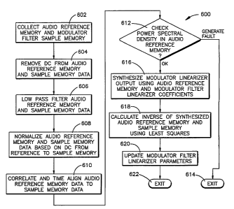
Reference is now made to Fig. 5 which illustrates the
routine involved for signal processing in the DSP for
modulator filter linearization. This procedure commences with
step 602, during which it collects audio samples from the
reference memory 8 and modulator filter output samples from
the sample memory 10.
The procedure advances to step 604 during which a process
removes the DC level from the audio samples obtained from
reference memory 8 and the DC level from the samples obtained
from the sample memory 10. The procedure advances to step
606.
In step 606, the processor provides a low pass filter
that filters the audio samples taken from the reference memory
and the samples obtained from the sample memory data and the
procedure advances to step 608.
In step 608, the processor normalizes the audio samples
taken from the reference memory and the filter samples taken
from the sample memory data based on the DC gain from the
reference to sample memories. The procedure then advances to
step 610.
In step 610, the processor correlates and time aligns the
audio data in the reference memory and the data stored in the
sample memory. The procedure then advances to step 612.
In step 612, the processor determines whether the power
spectral density in the audio reference memory is at a proper
level. If not, the processor generates a fault and the
-10-
CA 02529698 2005-12-15
WO 2005/002071 PCT/US2004/013791
procedure exits at step 614. If the determination is okay,
that procedure advances to step 616.
In step 616, the processor synthesizes the modulator
linearizer output using the audio reference memory and the
modulator filter linearizer coefficients. Procedure then
advances to step 618.
In step 618, the processor calculates the inverse of the
synthesized audio frequency memory and sample memory employing
least squares. The procedure then advances to step 620.
In step 620, the processor updates the modulator filter
linearizer parameters employed in the adaptive FIR filter
provided in the modulator filter linearizer 24. The procedure
then exits at step 622.
Reference is now made to Fig. 6, which illustrates the
signal processing that takes place to provide AM/AM pre-
correction. Then procedure 400 commences at step 402. In
this step, the processor collects audio data from the
reference memory 8 and RF output data from the sample memory
10. The procedure, then advances to step 404.
In step 404, the processor down converts the RF output
sample signal to base band and extracts the magnitude. The
procedure then advances to step 406.
In step 406, the processor low pass filters the audio
data taken from the reference memory 8 and the extracted
magnitude. The procedure then advances to step 408.
In step 408, the processor normalizes the audio data
obtained from the reference memory and magnitude data based on
the AC gain from the reference to magnitude data. The
procedure then advances to step 410.
In step 410 the processor correlates and time aligns the
reference memory data to magnitude data. The procedure then
advances to the decision step 412.
In the decision step 412, the processor checks the power
spectral density and peak levels in the audio data taken from
-11-
CA 02529698 2005-12-15
WO 2005/002071 PCT/US2004/013791
the reference memory to determine if the test tone has enough
bandwidth and amplitude variations. If not, a fault is
generated and the procedure advances to exit step 414.
If a positive determination was made at step 412, then
the procedure advances to step 416. In this step, the
processor calculates the inverse of the reference memory and
magnitude using least squares. The procedure advances to step
418.
In step 418, the processor updates the AM/AM pre-
correction parameters employed in the pre-correction 23 and
the procedure exits at step 420.
Reference is now made to Fig. 7 which is a flow diagram
illustrating the signal processing that takes place in
conjunction with the AM/PM pre-correction. This routine
commences at step 502 during which the processor collects RF
carrier and audio data from the reference memory and the RF
output sample memory. The procedure then advances to step
504.
In step 504, the processor down converts the RF output
from the sample memory and the RF carrier from the reference
memory to baseband. The procedure then advances to step 506.
In step 506, the processor computes the delay in the
audio data obtained from the reference memory to the RF output
data obtained from the sample memory as T1. The procedure
then advances to step 508.
In step 508, the processor computes the delay from the RF
carrier data obtained from the reference memory to the RF
output data obtained from the sample memory as T2. The
procedure then advances to step 510.
In step 510, the processor predistorts the RF carrier
from the reference memory by the phase pre-correction function
that has been determined by the DSP. The procedure then
advances to step 512.
-12-
CA 02529698 2005-12-15
WO 2005/002071 PCT/US2004/013791
In step 512, the processor calculates the angle from the
predistorted RF carrier from the reference memory and the RF
output from the sample memory using T2. The procedure then
advances to step 514.
In step 514, the processor unwraps the angle to get the
absolute phase. The procedure then advances to step 516.
In step 516, the processor time aligns the audio from the
reference memory to the angle using T1. The procedure then
advances to step 518.
In step 518, the processor provides low pass filtering of
the angle and the audio reference memory. The procedure then
advances to step 520.
In step 520, the processor removes the DC level from the
angle samples. The procedure then advances to step 522.
l5 In step 522, the processor solves direct problem using
least squares (LS). The procedure then advances to step 524.
In step 524, the processor updates the AM/PM pre-
corrector using the negative angle function obtained in LS.
The procedure then advances to exit at step 526.
-13-