Note: Descriptions are shown in the official language in which they were submitted.
CA 02541531 2006-04-11
Method and System For Compensation of Non-Uniformities in Light Emitting
Device
Displays
FIELD OF INVENTION
[0001 ] The present invention relates to display technologies, more
specifically a
method and system for compensating for non-uniformities of elements in light
emitting device displays.
BACKGROUND OF THE INVENTION
[0002] Active-Matrix Organic Light-Emitting Diode (AMOLED) displays are well
known art. Amorphous silicon is, for example, one of promising materials for
the
AMOLED displays, due to its low cost and vast installed infrastructure from
TFT-
LCD fabrication.
[0003] All AMOLED displays, regardless of backplane technology used, exhibit
differences in luminance on a pixel to pixel basis, primarily as a result of
process or
construction inequalities, or from aging caused by operational use over time.
Luminance non-uniformities in a display may also arise from natural
differences in
chemistry and performance from the OLED materials themselves. These non-
uniformities must be managed by the AMOLED display electronics in order for
the
display device to attain commercially acceptable levels of performance for
mass-
market use.
[0004] Figure 1 illustrates an operational flow of a conventional AMOLED
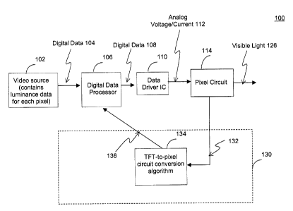
display
I0. Referring to Figure 1, a video source 12 contains luminance data for each
pixel
and sends the luminance data in the form of digital data 14 to a digital data
processor
I6. The digital data processor 16 may perform some data manipulation
funcrions,
such as scaling the resolution or changing the color of the display. The
digital data
processor 16 sends digital data 18 to a data driver IC 20. The data driver IC
20
converts that digital data 18 into an analog voltage or current 22, which is
sent to Thin
Film Transistors (TFTs) 26 in a pixel circuit 24. The TFTs 26 convert that
voltage or
current 22 into another current 28 which flows through an Organic Light-
Emitting
Diode (OLED) 30. The OLED 30 converts the current 28 into visible light 36.
The
OLED 30 has an OLED voltage 32, which is the voltage drop across the OLED. The
CA 02541531 2006-04-11
OLED 30 also has an efficiency 34, which is a ratio of the amount of light
emitted to
the current through the OLED.
[0005] The digital data 14, analog voltage/current 22, current 28, and visible
light 36
all contain the exact same information (i.e. luminance data). They are simply
different formats of the initial luminance data that came from the video
source 12.
The desired operation of the system is for a given value of luminance data
from the
video source 12 to always result in the same value of the visible light 36.
[0006] However, there are several degradation factors which may cause errors
on the
visible light 36. With continued usage, the TFTs 26 will output lower current
28 for
the same input from the data driver IC 20. With continued usage, the OLED 30
will
consume greater voltage 32 for the same input current. Because the TFT 26 is
not a
perfect current source, this will actually reduce the input current 28
slightly. With
continued usage, the OLED 30 will lose efficiency 34, and emit less visible
light for
the same input current.
[0007] Due to these degradation factors, the visible light output 36 will be
less over
time, even with the same luminance data being sent from the video source 12.
Depending on the usage of the display, different pixels may have different
amounts of
degradation.
[0008] Therefore, there will be an ever-increasing error between the required
brightness of some pixels as specified by the luminance data in the video
source 12,
and the actual brightness of the pixels. The result is that the desired image
will not
show properly on the display.
[0009] One way to compensate for these problems is to use a feedback loop.
Figure 2
illustrates an operational flow of a conventional AMOLED display 40 which
includes
the feedback loop. Refernng to Figure 2, a light detector 42 is employed to
directly
measure the visible light 36. The visible light 36 is converted into a
measured signal
44 by the light detector 42. A signal converter 46 converts the measured
visible light
signal 44 into a feedback signal 48. The signal converter 46 may be an analog-
to-
digital converter, a digital-to-analog converter, a microcontroller, a
transistor, or
another circuit or device. The feedback signal 48 is used to modify the
luminance
-2-
CA 02541531 2006-04-11
data at some point along its path, such as an existing component (e.g. 12, 16,
20, 26,
30), a signal line between components (e.g. 14, 18, 22, 28, 36), or
combinations
thereof.
[0010] Some modifications to existing components, and/or additional circuits
may be
required to allow the luminance data to be modified based on the feedback
signal 48
from the signal converter 46. If the visible light 36 is lower than the
desired
luminance from video source 12, the luminance signal may be increased to
compensate for the degradation of the TFT 26 or the OLED 30. This results in
that
the visible light 36 will be constant regardless of the degradation. This
compensation
scheme is often known as Optical Feedback (OFB). However, in the system of
Figure
2, the light detector 42 must be integrated onto a display, usually within
each pixel
and coupled to the pixel circuitry. Not considering the inevitable issues of
yield when
integrating a light detector into each pixel, it is desirable to have a light
detector which
does not degrade itself, however such light detectors are costly to implement,
and not
compatible with currently installed TFT-LCD fabrication infrastructure.
[0011 ] 'Therefore, there is a need to provide a method and system which can
compensate for non-uniformities in displays without measuring a light signal.
SUMMARY OF THE INVENTION
[0012] It is an object of the invention to provide a method and system that
obviates or
mitigates at least one of the disadvantages of existing systems.
[0013] In accordance with an aspect of the present invention there is provided
a
system for compensating non-uniformities in a light emitting device display
which
includes a plurality of pixels and a source for providing pixel data to each
pixel
circuit, which includes: a module for modifying the pixel data applied to one
or more
than one pixel circuit, including: an estimating module for estimating a
degradation of
a first pixel circuit based on measurement data read from a part of the first
pixel
circuit; and a compensating module for correcting the pixel data applied to
the first or
a second pixel circuit based on the estimation of the degradation of the first
pixel
circuit.
-3-
CA 02541531 2006-04-11
[0014] In accordance with a further aspect of the present invention there is
provided a
method of compensating non-uniformities in a light emitting device display
having a
plurality of pixels, including the steps of estimating a degradation of the
first pixel
circuit based on measurement data read from a part of the first pixel circuit;
and
correcting pixel data applied to the first or a second pixel circuit based on
the
estimation of the degradation of the first pixel circuit.
[0015] This summary of the invention does not necessarily describe all
features of the
invention.
BRIEF DESCRIPTION OF THE DRAWINGS
[0016] These and other features of the invention will become more apparent
from the
following description in which reference is made to the appended drawings
wherein:
[0017] Figure 1 illustrates a conventional AMOLED system;
[0018] Figure 2 illustrates a conventional AMOLED system which includes a
light
detector and a feedback scheme which uses the signal from the light detector;
[0019] Figure 3 illustrates a light emitting display system to which a
compensation
scheme in accordance with an embodiment of the present invention is applied;
[0020] Figure 4 illustrates an example of the light emitting display system of
Figure 3;
[0021 ] Figure 5 illustrates an example of a pixel circuit of Figure 4;
[0022] Figure 6 illustrates a further example of the light emitting display
system of
Figure 3;
[0023] Figure 7 illustrates an example of a pixel circuit of Figure 6;
[0024] Figure 8 illustrates an example of modules for the compensation scheme
applied to the system of Figure 4;
[0025] Figure 9 illustrates an example of a lookup table and a compensation
algorithm
module of Figure 7;
-4-
CA 02541531 2006-04-11
[0026] Figure 10 illustrates an example of inputs to a TFT-to-pixel circuit
conversion
algorithm module;
[0027] Figures 1 lA-11E illustrate experimental results of the compensation
scheme
applied to the system of Figure 3; and
[0028] Figure 12 illustrates an example of grayscale compression algorithm.
DETAILED DESCRIPTION
[0029] Embodiments of the present invention are described using an AMOLED
display which includes a pixel circuit having TFTs and an OLED. However, the
transistors in the pixel circuit may be fabricated using amorphous silicon,
nano/micro
crystalline silicon, poly silicon, organic semiconductors technologies (e.g.
organic
TFT), NMOS technology, CMOS technology (e.g. MOSFET), or combinations
thereof. The transistors may be a p-type transistor or n-type transistor. The
pixel
circuit may include a light emitting device other than OLED. In the
description
below, "pixel" and "pixel circuit" may be used interchangeably.
[0030] Figure 3 illustrates the operation of a light emitting display system
100 to
which a compensation scheme in accordance with an embodiment of the present
invention is applied. A video source 102 contains luminance data for each
pixel and
sends the luminance data in the form of digital data 104 to a digital data
processor
106. The digital data processor 16 may perform some data manipulation
functions,
such as scaling the resolution or changing the color of the display. The
digital data
processor 106 sends digital data 108 to a data driver IC 110. The data driver
IC 110
converts that digital data 108 into an analog voltage or current 112. The
analog
voltage or current 112 is applied to a pixel circuit 114. The pixel circuit
114 includes
TFTs and an OLED. The pixel circuit 114 outputs a visible light 126 based on
the
analog voltage or current 112.
[0031 ] In Figure 3, one pixel circuit is shown as an example. However, the
light
emitting display system 100 includes a plurality of pixel circuits. The video
source
102 may be similar to the video source I2 of Figures l and 2. The data driver
IC 110
may be similar to the data driver IC 20 of Figures 1 and 2.
-5-
CA 02541531 2006-04-11
[0032) A compensation functions module 130 is provided to the display. The
compensation functions module 130 includes a module 134 for implementing an
algorithm (referred to as TFT-to-pixel circuit conversion algorithm) on
measurement
132 from the pixel circuit 114 (referred to as degradation data, measured
degradation
data, measured TFT degradation data or measured TFT and OLED degradation
data),
and outputs calculated pixel circuit degradation data 136. It is noted that in
the
description below, "TFT-to-pixel circuit conversion algorithm module" and "TFT-
to-
pixel circuit conversion algorithm" may be used interchangeably.
[0033] The degradation data 132 is electrical data which represents how much a
part
of the pixel circuit 114 has been degraded. The data measured from the pixel
circuit
114 may represent, for example, one or more characteristics of a part of the
pixel
circuit 114.
[0034] The degradation data 132 is measured from, for example, one or more
thin-
filin-transistors (TFTs), an organic light emitting device (OLED), or a
combination
thereof. It is noted that the transistors of the pixel circuit 114 is not
limited to the
TFTs, and the light emitting device of the pixel circuit 14 is not limited to
the OLED.
The measured degradation data 132 may be digital or analog data. The system
100
provides compensation data based on measurement from a part of the pixel
circuit
(e.g. TFT) to compensate for non-uniformities in the display. The non-
uniformities
may include brightness non-uniformity, color non-uniformity, or a combination
thereof. Factors for causing such non-uniformities may include, but not
limited to,
process or construction inequalities in the display, aging of pixel circuits,
etc.
[0035] The degradation data 132 may be measured at a regular timing or a
dynamically regulated timing. The calculated pixel circuit degradation data
136 may
be compensation data to correct non-uniformities in the display. The
calculated pixel
circuit degradation data 136 may include any parameters to produce the
compensation
data. The compensation data may be used at a regular timing (e.g, each frame,
regular
interval, etc) or dynamically regulated timing The measured data, compensation
data
or a combination thereof may be stored in a memory (e.g. 142 of Figure 8).
-6-
CA 02541531 2006-04-11
[0036] The TFT-to-pixel circuit conversion algorithm module 134 or the
combination
of the TFT-to-pixel circuit conversion algorithm module 134 and the digital
data
processor 106 estimates the degradation of the entire pixel circuit based on
the
measured degradation data I32. Based on this estimation, the entire
degradation of
the pixel circuit 114 is compensated by adjusting, at the digital data
processor 106, the
luminance data (digital data 104) applied to a certain pixel circuit(s).
[0037] The system 100 may modify or adjust luminance data I04 applied to a
degraded pixel circuit or non-degraded pixel circuit. For example, if a
constant value
of visible light 126 is desired, the digital data processor 106 increases the
luminance
data for a pixel that is highly degraded, thereby compensating for the
degradation.
[0038] In Figure 3, the TFT-to-pixel circuit conversion algorithm module 134
is
provided separately from the digital data processor 106. However, the TFT-to-
pixel
circuit conversion algorithm module 134 may be integrated into the digital
data
processor 106.
[0039] Figure 4 illustrates an example of the system 100 of Figure 3. The
pixel
circuit 114 of Figure 4 includes TFTs 116 and OLED 120. The analog voltage or
current 112 is provided to the TFTs 116. The TFTs I 16 convert that voltage or
current 112 into another current 1 I8 which flows through the OLED 120. The
OLED
120 converts the current 118 into the visible light 126. The OLED 120 has an
OLED
voltage 122, which is the voltage drop across the OLED. The OLED 120 also has
an
efficiency 134, which is a ratio of the amount of light emitted to the current
through
the OLED 120.
[0040] The system 100 of Figure 4 measures the degradation of the TFTs only.
The
degradation of the TFTs 116 and the OLED 120 are usage-dependent, and the TFTs
116 and the OLED 120 are always linked in the pixel circuit 114. Whenever the
TFT
116 is stressed, the OLED 120 is also stressed. Therefore, there is a
predictable
relationship between the degradation of the TFTs 116, and the degradation of
the pixel
circuit 114 as a whole. The TFT-to-pixel circuit conversion algorithm module
134 or
the combination of the TFT-to-pixel circuit conversion algorithm module 134
and the
digital data processor 106 estimates the degradation of the entire pixel
circuit based on
CA 02541531 2006-04-11
the TFT degradation only. The embodiment of the present invention may also be
applied to systems that monitor both TFT and OLED degradation independently.
[0041 ] The pixel circuit 114 has a component that can be measured. The
measurement obtained from the pixel circuit 114 is in some way related to the
pixel
circuit's degradation.
[0042] Figure 5 illustrates an example of the pixel circuit 114 of Figure 4.
The pixel
circuit 114 of Figure 5 is a 4-T pixel circuit. The pixel circuit 1 I4A
includes a
switching circuit having TFTs 150 and 152, a reference TFT 154, a drive TFT
156, a
capacitor 1 S 8, and an OLED 160.
[0043] The gate of the switch TFT 1 SO and the gate of the feedback TFT 152
are
connected to a select line Vsel. The fwst terminal of the switch TFT 154 and
the first
terminal of the feedback TFT 152 are connected to a data line Idata. The
second
terminal of the switch TFT 150 is connected to the gate of the reference TFT
154 and
the gate of the drive TFT 156. The second terminal of the feedback TFT 152 is
connected to the first terminal of the reference TFT 154. The capacitor 158 is
connected between the gate of the drive TFT 156 and ground. The OLED 160 is
connected between voltage supply Vdd and the drive TFT 156. The OLED 160 may
also be connected between drive TFT 156 and ground in other systems (i.e.
drain-
connected format).
[0044] When programming the pixel circuit 114A, Vsel is high and a voltage or
current is applied to the data line Idata. The data Idata initially flows
through the TFT
150 and charges the capacitor 158. As the capacitor voltage rises, the TFT 154
begins
to turn on and Idata starts to flow through the TFTs 152 and 154 to ground.
The
capacitor voltage stabilizes at the point when all of Idata flows through the
TFTs 152
and 154. The current flowing through the TFT 154 is mirrored in the drive TFT
156.
[0045] In the pixel circuit 114A, by setting Vsel to high and putting a
voltage on
Idata, the current flowing into the Idata node can be measured. Alternately,
by setting
Vsel to high and putting a current on Idata, the voltage at the Idata node can
be
measured. As the TFTs degrade, the measured voltage (or current) will change,
allowing a measure of the degradation to be recorded. In this pixel circuit,
the analog
_g_
CA 02541531 2006-04-11
voltage/current 112 shown in Figure 4 is connected to the Idata node. The
measurement of the voltage or current can occur anywhere along the connection
between the data driver IC 110 and the TFTs I 16.
[0046) In Figure 4, the TFT-to-pixel circuit conversion algorithm is applied
to the
measurement 132 from the TFTs 116. However, current/voltage information read
from various places other than TFTs 116 may be usable. For example, the OLED
voltage 122 may be included with the measured TFT degradation data 132
[0047] Figure 6 illustrates a further example of the system I00 of Figure 3.
The
system 100 of Figure 6 measures the OLED voltage 122. Thus, the measured data
132
is related to the TFT 116 and OLED 120 degradation ( "measured TFT and OLED
voltage degradation data 132A" in Figure 6). The compensation functions module
130 of Figure 6 implements the TFT-to-pixel circuit conversion algorithm 134
on the
signal related to both the TFT degradation and OLED degradation. The TFT-to-
pixel
circuit conversion algorithm module 134 or the combination of the TFT-to-pixel
circuit conversion algorithm module 134 and the digital data processor 106
estimates
the degradation of the entire pixel circuit based on the TFT degradation and
the OLED
degradation. The TFT degradation and OLED degradation may be measured
separately and independently.
[0048] Figure 7 illustrates an example of the pixel circuit 114 of Figure 6.
The pixel
circuit 1148 of Figure 7 is a 4-T pixel circuit. The pixel circuit 1148
includes a
switching circuit having TFTs 170 and 172, a reference TFT 174, a drive TFT
176, a
capacitor 178, and an OLED 180.
[0049) The gate of the switch TFT 170 and the gate of tine switch TFT 172 are
connected to a select line Vsel. The first terminal of the switch TFT 172 is
connected
to a data line Idata while the first terminal of the switch TFT 170 is
connected to the
second terminal of the switch TFT 172 which is connected to the gate of the
reference
TFT 174 and the gate of the drive TFT 176. The second terminal of the switch
TFT
170 is connected to the first terminal of the reference TFT 174. The capacitor
178 is
connected between the gate of the drive TFT 176 and ground. The first terminal
of
the drive TFT 176 is connected to voltage supply Vdd. The second terminal of
the
-9-
CA 02541531 2006-04-11
reference TFT 174 and the second terminal of the drive TFT I76 are connected
to the
OLED I 80.
[0050] When programming the pixel circuit 114B, Vsel is high and a voltage or
current is applied to the data line Idata. The data Idata initially flows
through the TFT
172 and charges the capacitor 178. As the capacitor voltage rises, the TFT 174
begins
to turn on and Idata starts to flow through the TFTs 170 and 174 and OLED 180
to
ground. The capacitor voltage stabilizes at the point when all of Idata flows
through
the TFTs 152 and 154. The current flowing through the TFT 154 is mirrored in
the
drive TFT 156. In the pixel circuit 114A, by setting Vsel to high and putting
a voltage
on Idata, the current flowing into the Idata node can be measured.
Alternately, by
setting Vse1 to high and putting a current on Idata, the voltage at the Idata
node can be
measured. As the TFTs degrade, the measured voltage (or current) will change,
allowing a measure of the degradation to be recorded. It is noted that unlike
the pixel
circuit 114A of Figure 5, the current now flows through the OLED I 80.
Therefore the
measurement made at the Idata node is now partially related to the OLED
Voltage,
which will degrade over time. In the pixel circuit 114B, the analog
voltage/current
112 shown in Figure 6 is connected to the Idata node. The measurement of the
voltage or current can occur anywhere along the connection between the data
driver
IC 1 IO and the TFTs 116.
[0051 ) Referring to Figures 3, 4 and 6, the pixel circuit 114 may allow the
current out
of the TFTs 116 to be measured, and to be used as the measured TFT degradation
data
132. The pixel circuit 114 may allow some part of the OLED efficiency to be
measured, and to be used as the measured TFT degradation data 132. The pixel
circuit 114 may also allow a node to be charged, and the measurement may be
the
time it takes for this node to discharge, The pixel circuit 114 may allow any
parts of it
to be electrically measured. Also, the dischargelcharge level during a given
time can
be used for aging detection.
[0052) Referring to Figure 8, an example of modules for the compensation
scheme
applied to the system of Figure 4 is described. The compensation functions
module
130 of Figure 8 includes an analog/digital (A/D) converter I40. The A/D
converter
140 converts the measured TFT degradation data 132 into digital measured TFT
CA 02541531 2006-04-11
degradation data 132B. The digital measured TFT degradation data 132B is
converted
into the calculated pixel circuit degradation data 136 at the TFT-to-Pixel
circuit
conversion algorithm module 134. The calculated pixel circuit degradation data
136
is stored in a lookup table 142. Since measuring TFT degradation data from
some
pixel circuits may take a long time, the calculated pixel circuit degradation
data 136 is
stored in the lookup table 142 for use.
[0053] In Figure 8, the TFT-to-pixel circuit conversion algorithm 134 is a
digital
algorithm. The digital TFT-to-pixel circuit conversion algorithm 134 may be
implemented, for example, on a microprocessor, an FPGA, a DSP, or another
device,
but not limited to these examples. The lookup table 142 may be implemented
using
memory, such as SRAM or DRAM. This memory may be in another device, such as a
microprocessor or FPGA, or may be an independent device.
[0054] The calculated pixel circuit degradation data 136 stored in the lookup
table
142 is always available for the digital data processor 106. Thus, the TFT
degradation
data 132 for each pixel does not have to be measured every time the digital
data
processor 106 needs to use the data. The degradation data 132 may be measured
infrequently (for example, once every 20 hours, or less). Using a dynamic time
allocation for the degradation measurement is another case, more frequent
extraction
at the beginning and less frequent extraction after the aging gets saturated.
[0055] The digital data processor 106 may include a compensation module 144
for
taking input luminance data for the pixel circuit 114 from the video source
102, and
modifying it based on degradation data for that pixel circuit or other pixel
circuit. In
Figure 8, the module 144 modifies luminance data using information from the
lookup
table 142.
[0056] It is noted that the configuration of Figure 8 is applicable to the
system of
Figures 3 and 6. It is noted that the lookup table I42 is provided separately
from the
compensating functions module 130, however, it may be in the compensating
functions module 130. It is noted that the lookup table 142 is provided
separately
from the digital data processor 106, however, it may be in the digital data
processor
106.
CA 02541531 2006-04-11
[0057] One example of the lookup table 142 and the module 144 of the digital
data
processor 106 is illustrated in Figure 9. Referring to Figure 9, the output of
the TFT-
to-pixel circuit conversion algorithm module 134 is an integer value. This
integer is
stored in a lookup table 142A (corresponding to 142 of Figure 8). Its location
in the
lookup table 142A is related to the pixel's location on the AMOLED display.
Its
value is a number, and is added to the digital luminance data 104 to
compensate for
the degradation.
[0058] For example, digital luminance data may be represented to use 8-bits
(256
values) for the brightness of a pixel. A value of 256 may represent maximum
luminance for the pixel. A value of 128 may represent approximately 50%
luminance.
The value in the lookup table I42A may be the number that is added to the
luminance
data 104 to compensate for the degradation. Therefore, the compensation module
(144 of Figure 7) in the digital data processor 106 may be implemented by a
digital
adder 144A. It is noted that digital luminance data may be represented by any
number
of bits, depending on the driver IC used (for example, 6-bit, 8-bit, 10-bit,
14-bit, etc).
[0059] In Figures 3, 4, 6, $ and 9, the TFT-to-pixel circuit conversion
algorithm
module 134 has the measured TFT degradation data 132 or 132A as an input, and
the
calculated pixel circuit degradation data 136 as an output. However, there may
be
other inputs to the system to calculate compensation data as well, as shown in
Figure
10. Figure 10 illustrates an example of inputs to the TFT-pixel circuit
conversion
algorithm module 134. In Figure I0, the TFT-to-pixel circuit conversion
algorithm
module 134 processes the measured data (132 of Figures 3, 4, 8 and 9, 132A of
Figure
6, 132B of Figures 8 and 9) based on additional inputs 190 (e.g. temperature,
other
voltages etc), empirical constants 192 or combinations thereof.
[0060] The additional inputs 190 may include measured parameters such as
voltage
reading from current-programming pixels and current reading from voltage-
programming pixels. These pixels may be different from a pixel circuit from
which
the measured signal is obtained. For example, a measurement is taken from a
"pixel
under test" and is used in combination with another measurement from a
"reference
pixel". As described below, in order to determine how to modify luminance data
to a
pixel, data from other pixels in the display may be used. The additional
inputs 190
CA 02541531 2006-04-11
may include light measurements, such as measurement of an ambient light in a
mom.
A discrete device or some kind of test structure around the periphery of the
panel may
be used to measure the ambient light. The additional inputs may include
humidity
measurements, temperature readings, mechanical stress readings, other
environmental
stress readings, and feedback from test structures on the panel.
[0061] It may also include empirical parameters 192, such as the brightness
loss in the
OLED due to decreasing efficiency (Oh), the shift in OLED voltage over time
(OVoled), dynamic effects of Vt shift, parameters related to TFT performance
such as
Vt, ~Vt, mobility (p.), inter-pixel non-uniformity, DC bias voltages in the
pixel circuit,
changing gain of current-mirror based pixel circuits, short-term and long-term
based
shifts in pixel circuit performance, pixel-circuit operating voltage variation
due to IR-
drop and ground bounce.
[0062) Referring to Figures 8 and 9, the TFT-to-pixel-circuit conversion
algorithm in
the module 134 and the compensation algorithm 144 in the digital data
processor 106
work together to convert the measured TFT degradation data 132 into a
luminance
correction factor. The luminance correction factor has information about how
the
luminance data for a given pixel is to be modified, to compensate for the
degradation
in the pixel.
[0063) In Figure 9, the majority of this conversion is done by the TFT-to-
pixel-circuit
conversion algorithm module 134. It calculates the luminance correction values
entirely, and the digital adder 144A in the digital data processor 106 simply
adds the
luminance correction values to the digital luminance data 104. However, the
system
100 may be implemented such that the TFT-to-pixel circuit conversion algorithm
module 134 calculates only the degradation values, and the digital data
processor 106
calculates the luminance correction factor from that data. The TFT-to-pixel
circuit
conversion algorithm 134 may employ fuzzy logic, neural networks, or other
algorithm structures to convert the degradation data into the luminance
correction
factor.
[0064] The value of the luminance correction factor may allow the visible
light to
remain constant, regardless of the degradation in the pixel circuit. The value
of the
-13
CA 02541531 2006-04-11
luminance correction factor may allow the luminance of degraded pixels not to
be
altered at all; instead, the luminance of the non-degraded pixels to be
decreased. In
this case, the entire display may gradually lose luminance over time, however
the
uniformity may be high.
[0065] The calculation of a luminance correction factor may be implemented in
accordance with a compensation of non-uniformity algorithm, such as a constant
brightness algorithm, a decreasing brightness algorithm, or combinations
thereof. The
constant brightness algorithm and the decreasing brightness algorithm may be
implemented on the TFT-to-pixel circuit conversion algorithm module (e.g. 134
of
Figure 3) or the digital data processor (e.g. 106 of Figure 3). The constant
brightness
algorithm is provided for increasing brightness of degraded pixels so as to
match non-
degraded pixels. The decreasing brightness algorithm is provided for
decreasing
brightness of non-degraded pixels 244 so as to match degraded pixels. These
algorithm may be implemented by the TFT-to-pixel circuit conversion algorithm
module, the digital data processor (such as 144 of Figure 8), or combinations
thereof.
It is noted that these algorithms are examples only, and the compensation of
non-
uniformity algorithm is not limited to these algorithms.
[0066] Referring to 11A-11E, the experimental results of the compensation of
non-
uniformity algorithms are described in detail. Under the experiment, an AMOLED
display includes a plurality of pixel circuits, and is driven by a system as
shown in
Figures 3, 4, 6, 8 and 9. It is noted that the circuitry to drive the AMOLED
display is
not shown in Figures 1 lA-11E.
[0067] Figure 1 lA schematically illustrates an AMOLED display 240 which
starts
operating (operation period t~ hour). The video source ( 102 of Figures 3, 4,
7, 8 and
9) initially outputs maximum luminance data to each pixel. No pixels are
degraded
since the display 240 is new. The result is that all pixels output equal
luminance and
thus all pixels show uniform luminance.
[0068] Next, the video source outputs maximum luminance data to some pixels in
the
middle of the display as shown in Figure 11 B. Figure 11 B schematically
illustrates
the AMOLED display 240 which has operated for a certain period where maximum
-~ 4
CA 02541531 2006-04-11
luminance data is applied to pixels in the middle of the display. The video
source
outputs maximum luminance data to pixels 242, while it outputs minimum
luminance
data (e.g. zero luminance data) to pixels 244 around the outside of the pixels
242. It
maintains this for a long period of time, for example 1000 hours. The result
is that the
pixels 242 at maximum luminance will have degraded, and the pixels 244 at zero
luminance will have no degradation.
[0069] At 1000 hours, the video source outputs maximum luminance data to all
pixels. The results are different depending on the compensation algorithm
used, as
shown in Figures 11C-11E.
[0070] Figures 11C schematically illustrates the AMOLED display 240 to which
no-
compensation algorithm is applied. As shown in Figure 11C, if there was no
compensation algorithm, the degraded pixels 242 would have a lower brightness
than
the non-degraded pixels 244.
[0071] Figures 11D schematically illustrates the AMOLED display 240 to which
the
constant brightness algorithm is applied. The constant brightness algorithm is
implemented for increasing luminance data to degraded pixels, such that the
luminance data of the degraded pixels matches that of non-degraded pixels. For
example, the increasing brightness algorithm provides increasing currents to
the
stressed pixels 242, and constant current to the unstressed pixels 244. Both
degraded
and non-degraded pixels have the same brightness. Thus, the display 240 is
uniform.
Differential aging is compensated, and brightness is maintained, however more
current is required. Since the current to some pixels is being increased, this
will cause
the display to consume more current over time, and therefore more power over
time
because power consumption is related to the current consumption.
[0072] Figures 1 lE schematically illustrates the AMOLED display 240 to which
the
decreasing brightness algorithm is applied. The decreasing brightness
algorithm
decreases luminance data to non-degraded pixels, such that the luminance data.
of the
non-degraded pixels match that of degraded pixels. For example, the decreasing
brightness algorithm provides constant OLED current to the stressed pixels
242, while
decreasing current to the unstressed pixels 244. Both degraded and non-
degraded
CA 02541531 2006-04-11
pixels have the same brightness. Thus, the display 240 is uniform.
Differential aging
is compensated, and it requires a lower Vsupply, however brightness decrease
over
time. Because this algorithm does not increase the current to any of the
pixels, it will
not result in increased power consumption.
[0073] Referring to Figure 3, components, such as the video source 102 and the
data
driver IC 110, may use only 8-bits, or 256 discrete luminance values.
Therefore if the
video source 102 outputs maximum brightness (a luminance value of 255), there
is no
way to add any additional luminance, since the pixel is already at the maximum
brightness supported by the components in the system. Likewise, if the video
source
102 outputs minimum brightness (a luminance value of 0), there is no way to
subtract
any luminance. The digital data processor 106 may implement a grayscale
compression algorithm to reserve some grayscales. Figure 12 illustrates an
implementation of the digital data processor 106 which includes a grayscale
compression algorithm module 250. The grayscale compression algorithm 250
takes
the video signal represented by 256 luminance values, and transforms it to use
less
luminance values. For example, instead of minimum brightness represented by
grayscale 0, minimum brightness may be represented by grayscale 50. Likewise,
instead of maximum brightness represented by grayscale 200. In this way, there
are
some grayscales reserved for future increase and decrease. It is noted that
the shift in
grayscales does not reflect the actual expected shift in grayscales.
[0074] According to the embodiments of the present invention, the scheme of
estimating (predicting) the degradation of the entire pixel circuit and
generating a
luminance correction factor ensures uniformiries in the display. According to
the
embodiments of the present invention, the aging of some components or entire
circuit
can be compensated, thereby ensuring uniformity of the display.
[0075] According to the embodiments of the present invention, the TFT-to-pixel
circuit conversion algorithm allows for improved display parameters, for
example,
including constant brightness uniformity and color uniformity across the panel
over
time. Since the TFT-to-pixel circuit conversion algorithm takes in additional
parameters, for example, temperature and ambient light, any changes in the
display
due to these additional parameters may be compensated for.
-16
CA 02541531 2006-04-11
[0076] The TFT-to-Pixel circuit conversion algorithm module (134 of Figures 3,
4, 6,
8 and 9), the compensation module (144 of Figure 8, 144A of Figure 9, the
compensation of non-uniformity algorithm, the constant brightness algorithm,
the
decreasing brightness algorithm and the grayscale compression algorithm may be
implemented by any hardware, software or a combination of hardware and
software
having the above described functions. The software code, instructions and/or
statements, either in its entirety or a part thereof, may be stored in a
computer readable
memory. Further, a computer data signal representing the software code,
instructions
and/or statements, which may be embedded in a Garner wave may be transmitted
via a
communication network. Such a computer readable memory and a computer data
signal and/or its carrier are also within the scope of the present invention,
as well as
the hardware, software and the combination thereof.
[0077] The present invention has been described with regard to one or more
embodiments. However, it will be apparent to persons skilled in the art that a
number
of variations and modifications can be made without departing from the scope
of the
invention as defined in the claims.