Note: Descriptions are shown in the official language in which they were submitted.
CA 02543151 2002-10-O1
GaN Substrate, Method Of Growing GaN And Method Of Producing GaN substrate
This is a divisional application of Canadian Patent Application Serial No.
2,406,347
filed on October I, 2002.
This invention relates to a single crystal gallium nitride (GaN) substrate, a
method of
growing single crystal GaN and a method of making a single crystal GaN
substrate utilized as
a substrate of making laser diodes (LDs) and light emitting diodes (LEDs)
composed of
groups 3-S nitride semiconductors.
It should be understood that the expression "the invention" and the like
encompasses
the subject matter of both the parent application and the divisional
application.
Light emitting devices based upon group 3-S nitride semiconductor include
blue/green
light emitting diodes and blue light laser diodes. Blue light LEDs have been
sold on the
market. But, LDs have not been on the market yet. Almost all of the
conventional 3-5 nitride
light emitting devices and laser diodes (LEDs, LDs) have been fabricated upon
sapphire ( cz -
A1203) substrates. Sapphire is a rigid and sturdy material. Sapphire excels in
chemical and
physical stability. Another advantage of sapphire is to allow GaN
heteroepitaxial growth on it.
Thus, GaN films, AIGaN films or InGaN films can be grown on sapphire
substrates. Sapphire
has been an exclusive, pertinent substrate for GaN type LEDs.
Sapphire, however, has some drawbacks as a substrate. Sapphire lacks cleavage.
Sapphire is not a semiconductor but an insulator. GaN films or InGaN films
grown on a
sapphire substrate are annoyed by large lattice misfitting. Lattice misfitting
means a
difference of lattice constants between a substrate and a film. Sapphire
belongs to trigonal
symmetry group. Sapphire lacks three-fold rotation symmetry and inversion
symmetry_ Poor
symmetry deprives sapphire of cleavage planes.
The use of sapphire substrates forces device makers to cut a processed GaN
wafer into
individual chips by mechanical dicing instead of natural cleavage. To dice a
hard, sturdy, rigid
sapphire plate mechanically into pieces is a difficult process, which
decreases yield and
CA 02543151 2002-10-O1
enhances cost.
Noncleavage further induces a serious di~culty of making good resonator
mirrors of
laser diodes. The resonators are made by mechanical polishing, which raises
the cost of LDs
and declines the quality of the resonators.
la
CA 02543151 2002-10-O1
Insulation is another weak point of sapphire. Insulating sapphire incurs a
difficulty of
n-electrodes. An insulating substrate forbids an LED from having an n-
electrode on the
bottom unlike an ordinary diode. An n-electrode is formed by etching away a
top p-GaN layer,
an active layer, revealing an intermediate n-GaN film on the sapphire
substrate, depositing an
5, n-metal electrode on the n-GaN film, and wirebonding the n-metal electrode
with a lead pin.
The etching for revealing the intermediate film and wirebonding are extra
steps which are
required for making an n-electrode on the on-sapphire device.
Current flows in a horizontal direction in the n~GaN film. The n-GaN film
should be
grown to a thick film for reducing electric resistivity of the n-GaN film.
Extra steps and extra
components raise the cost of fabrication.
Since two electrodes are formed on n- and p-films within a chip, an extra wide
area is
required for the chip. The wide, large chip raises cost up.
The third weak point of a sapphire substrate is lattice misfitting. Lattice
misfitting
induces high density dislocations into GaN epi-layers grown upon a sapphire
substrate. It is
said that GaN epi-layers of on-sapphire LEDs sold on the market should have 1
X 109cm-2
dislocations.
Another candidate for a substrate is silicon carbide SiC, since lattice misfit
between
SiC and GaN is smaller than the GaN/sapphire misfit. A GaN grown on a SiC
substrate turns
out to have a similar high dislocation density to the on-sapphire GaN layers.
SiC does not
surpass sapphire as a substrate.
High dislocation density in GaN, InGaN, AIGaN epi-layers causes no problem in
the
nitride-type LEDs because of low current density. In the case of LDs having a
narrow striped
electrode and a narrow emission area, high density current would reproduce
dislocations and
the increased dislocations would shorten the lifetime of LDs. Non-cleavage,
insulator and
misfit are three serious drawbacks of sapphire substrates.
2
CA 02543151 2002-10-O1
The best candidate for an ideal substrate for LDs is a gallium nitride (GaN)
single
crystal substrate. If a high quality GaN single crystal substrate were
obtained, the problem of
the lattice misfitting would be solved, because a device would take a GaN/GaN
homoepitaxy
structure.
A GaN crystal has cleavage planes {I-100}. Cleavability of GaN enables device
makers to divide a processed GaN wafer into individual chips along cleavage
planes.
Cleavage lowers the difficulty and cost of chip separation. Resonator minors
of LDs can be
easily produced by natural cleavage. High quality resonators are formed by the
cleavage.
GaN can be doped with n-type dopants or p-type dopants. Doping with an
impurity
can prepare a conductive GaN substrate. Since a low resistance n-type
substrate is made by
doping with an n-type dopant, an n-electrode can be formed at a bottom of an n-
GaN substrate.
Vertical electrode alignment enables an LD and an LED to reduce a chip size,
simplify a
device structure and curtail the cost.
However, GaN single crystals are not yielded as natural resources. Production
of GaN
single crystals is difficult. Manufacture of high quality GaN single crystal
substrates with a
practical size has been impossible till now.
It is said that ultrahigh pressure and ultrahigh temperature would realize
production of
a tiny GaN crystal grown from a mixture of melt/solid at thermal equilibrium.
The ultrahigh
pressure method is impractical. A wide GaN substrate cannot be made by the
method.
Methods of making GaN substrate crystals by growing a thick GaN crystal on a
foreign material substrate in vapor phase and eliminating the foreign material
substrate had
been proposed. The vapor phase method has been inherently a method for making
thin GaN,
AIGaN, InGaN films on a sapphire substrate. The vapor phase method was
diverted from film
piling to substrate production. The inherent vapor phase method is unsuitable
for substrate
production. Large inner stress and many dislocations appeared in the GaN films
made by the
3
CA 02543151 2002-10-O1
vapor phase method. Large inner stress prevented GaN films from growing thick
crystals
sufficient for substrates. A GaN "substrate" is a final product of the present
invention. A
substrate of a foreign material, e.g., sapphire or GaAs is a starting base
plate for making GaN.
Two substrates should not be confused. For discriminating two kinds of
substrates, the starting
foreign substrate is here named "undersubstrate".
The inventors of the present invention proposed an epitaxial lateral
overgrowth
method of growing a GaN via a mask on an undersubstrate in vapor phase (
l~Japanese Patent
Application No.9-298300, 20Japanese patent application No.lO-9008).
In the concrete, the ELO method proposed by us was a method of preparing a
GaAs
undersubstrate, producing an Si0 2 or SiN film on the GaAs undersubstrate,
perforating many
small windows regularly and periodically aligning with a short pitch (spatial
period), growing
a GaN film on the masked GaAs substrate in vapor phase for a long time, and
eliminating the
GaAs substrate. The ELO alleviates inner stress and dislocations. The
preceding ELO method
utilized sapphire as an undersubstrate, which may be called an on-sapphire
ELO. But, the
above ELO method made use of GaAs as an undersubstrate. The method of the
present
inventors is called here an on-GaAs ELO.
The inventors of the present invention have proposed a method of making a
plurality
of GaN substrates by homoepitaxially growing a thick GaN crystal upon a GaN
substrate
obtained by the former mentioned ELO method, making a tall GaN ingot and
slicing the tall
GaN ingot into a plurality of wafers (~3 Japanese Patent Application No.lO-
102546).
The improved ELO gave a probability for making wide GaN single crystal
substrates
on a commercial scale.
The ELO made GaN crystals were plagued with high dislocation density. The ELO
reduces dislocations at an early stage of the growth. During the long time
growth, however,
dislocations increase again. Bad quality prohibited the ELO-GaN substrate from
being the
4
CA 02543151 2002-10-O1
substrates for producing nitride type laser diodes (InGaN-LDs). Production of
high quality
(long lifetime) LDs required lower dislocation density GaN substrates.
Mass production of devices requires wide GaN substrates which have low
dislocation
density and high quality in a wide area.
. The inventors of the present invention proposed a method of making low
dislocation
density GaN substrate (~Japanese Patent Laying Open No.2001-102307). The
present
invention is an improvement of the former method ~.
The method proposed by ~ is now called "facet growth" method in short. The
method reduces dislocations by forming three-dimensional facets and facet pits
of e.g.,
reverse-hexagonal cones on a growing surface intentionally, maintaining the
facets and pits,
growing a GaN crystal without burying the pits, gathering dislocations by the
facets to the
bottom of the pits, and reducing dislocations in other regions except the pit
bottoms.
Three-dimensional facet pits are otherwise reverse-dodecagonal cones built by
facets.
The facets comprise typical { 11-22} and { 1-101 } planes.
The facet growth ~ (Japanese Patent Laying Open No.2001-102307) proposed by
the inventors grows a GaN crystal in vapor phase on the condition of making
facets and
maintains the facets without burying the pits of facets. The facets grow not
in the c-axis
direction but in a direction normal to the facets. The roles of facets and
pits in the facet
growth ~ (Japanese Patent Laying Open No.2001-102307) are described with
reference to
Fig.l which shows a small part around a facet pit on a surface of a GaN
crystal growing in the
facet growth. In practice, many facets and facet pits appear on the surface. A
vapor phase
epitaxy method (HVPE, MOCVD, MOC or Sublimation) grows a GaN crystal on a
substrate
in a direction of a c-axis. The growth is a c-axis direction growth but is not
a "C-plane
growth" which has been prevalent in the conventional GaN growth. Facets grow
in directions
normal to the facets.
5
CA 02543151 2002-10-O1
Conventional C-plane growth methods grow a GaN film epitaxially on a substrate
by
maintaining a smooth C-plane surface. Produced GaN crystals have poor quality
of high
dislocation density, for example, 10' °cm- 2. Our new facet growth
method intentionally
makes facets and pits, maintains the facets and reduces dislocations by make
the best use of
the function of facets of gathering dislocations into pit bottoms.
The facet growth produces plenty of reverse hexagonal cone pits 4 on the
growing
GaN surface. Fig.l shows only one of many pits. Six slanting planes are low
index facets 6
of { I 1-22} or { 1-101 } planes. A flat top surface 7 outside of the pit 4 is
a surface of C-plane
growth. In the pit, the facet grows inward in the direction of a normal
standing on the facet as
shown by inward arrows 9. Dislocations are swept to corner lines 8 by the
growing facet.
Dislocations are gathered on the six corner lines 8.
The dislocations swept to the corner lines 8 slide down along the corner lines
to the
bottom of the pit. In practice, the dislocations do not fall along the comer
lines 8. The growth
raised the facets, the corner lines and the pit bottoms at a definite speed.
Sliding dislocations
along the rising corner lines centrifugally move inward in horizontal
directions. Finally, the
dislocations attain to the center of the pit just at the time when the pit
bottom rises to the
height of the dislocation. Then, dislocations are accumulated at the bottom of
the pit. The
number of the dislocations on the facets is reduced by the accumulation of
dislocations at the
bottom.
Proceeding of the facet growth sometimes forms planar defects 10 following the
corner lines 8 by storing the swept dislocations at the comer lines. The
planar defects are six
planes with sixty degree rotation invariance corresponding with the hexagonal
symmetry of
GaN. The width of the planar defects 10 is equal to the diameter of the pit 4.
The six planar
defects 10 cross at a vertical extension of the pit bottom. The crossing line
forms a linear
defect assembly 11 having highly concentrated dislocation. Ideally all the
dislocations initially
6
CA 02543151 2002-10-O1
existing in the pit are swept to and are accumulated at the pit bottom. The
other parts 2 lose
dislocations and become low dislocation density single crystals. This is the
dislocation
reduction method proposed by ~ (Japanese Patent Laying Open No.2001-102307).
Finally, the majority of dislocations are concentrated to the pit center. The
operations
of the facets reduce dislocation density in the regions included within the
projection of the
pits.
There are some problems in the new facet growth method proposed by ~ which
makes facet pits at random spots accidentally, maintains the facet pits, grows
a GaN crystal
without burying the pits, and concentrates dislocations to the bottoms of the
facet pits.
Though the facets gather dislocations to the pit bottoms, dislocations are not
concentrated fully into a narrow, restricted spot. For example, when 100 ~c m
~ pits are
yielded, some pits can concentrate dislocations to a small spot at the bottom
of a several
micrometer diameter but other pits have about SO ~c m ~ hazy dislocation
dispersion region
of medium dislocation density near the bottom.
Fig.3 demonstrates the occurrence of the hazy dislocation dispersion. Fig.3(1)
shows
that a c-axis crystal growth having a C-plane 17 (arrows) moves facets 16
inward, dislocations
on the facets are carried by the facets 16 in horizontal directions (shown by
horizontal lines) to
the pit bottom and the bottom has a linear dislocation bundle 15. But,
repulsive forces release
once gathered dislocations outward. Fig. 3(2) shows that the once concentrated
dislocations
15 are diffusing from the bottom to the facet 16 of a pit 14. Occurrence of
hazy dislocation
dispersion is a drawback of the facet growth of ~.
If the pit size is enlarged for widening the area of good quality portions,
the area of the
hazy dislocation dispersion further dilates_ The reason is supposed that
enlargement of a pit
size increases the number of the dislocations gathered at the bottom and the
number of the
dislocations released from the bundle.
7
CA 02543151 2002-10-O1
The inventors think that the release of dislocations from the pit centers
results from
repulsion acting between concentrated dislocations. Unification of pits incurs
disorder of
dislocations and expansion of the hazy dispersion of dislocations. Excess
concentration
induces the hazy dislocation dispersion.
The hazy dislocation dispersion has about 2 X 10' cm- 2 dislocation density
which has
dependence to positions. Such a high dislocation density GaN substrate is
insufficient for
making laser diodes (LDs) of a satisfactory lifetime. A long lifetime of LDs
requires to reduce
dislocations down to one twentieth (1/20) of the current value (2 X 10'cm- 2)
, that is, to 1 X
IOscm-2
Another problem is the existence of planar defects 10 produced under the
corner lines
of pits as shown in Fig. l (b). The planar defects are radially arranged with
60 degree rotation
symmetry. Facets assemble dislocations at pit corner lines. Without
progressing to the center
bottom, the assembled dislocations form planar defects 10 by dangling from the
corner lines.
A planar defect can be considered as an alignment of dislocations in a plane.
The planar
defects are another problem of the conventional facet growth method. Sometimes
a slide of
crystal planes occurs on both sides of the planar defect.
Besides the 60 degree rotation symmetric planar defects, 30 degree rotation
symmetry
planar defects sometimes appear in dodecagonal pits on a growing surface.
Planar defects
appear as dislocation arrays on the surface of the growing substrate. Planar
defects are a
serious hindrance to produce long lifetime LDs. Prolongation of LD lifetime
requires
reduction of the planar defects.
The final problem is distribution of defects. Dislocation reduction of the
facet growth
method makes use of facet pits accidentally and randomly appearing on a facet
growth.
Positions of pits are not predetermined. Numbers of appearing pits are also
not programmable.
Positions, numbers, shapes and sizes of appearing pits are all stochastic,
random, accidental
8
CA 02543151 2002-10-O1
variables which are unpredeterminable, unprogrammable, uncontrollable. It is a
problem that
the positions of pits are uncontrollable.
If a plurality of laser diodes were fabricated upon a GaN substrate having
random
distributing planar defects, emission stripes of active layers of the laser
diodes would
accidentally coincide with the defect assemblies which occupy random spots on
the GaN
substrate. In the case of coincidence of the active layer with the defect
bundles, important
emission layers are plagued by the defect assemblies. Large current density
driving current
would invite rapid degeneration on emission stripes from the inherent defects
of the laser
diodes.
Uncontrollability of the positions of pits would decrease the yield of
manufacturing
laser diodes on the substrate.
Manufacturing GaN substrates for making laser diodes thereon requires
enhancement
of yield through controlling the positions of dislocation bundles on the GaN
substrates. It is
important to control the positions of dislocation bundles not to collide with
emission stripes of
laser diode chips on the GaN substrates.
Three problems have been described for long lifetime laser diodes. The purpose
of the
present invention is to conquer the three problems;
(I) Reduction of hazy dislocation diffusion from the pit center composed of
facets,
(2) Extinction of planar defects at the bottoms of the pits composed of
facets,
(3) Controlling of positions of the pits made of facets.
The present invention aims at overcoming the difficulties of the three
problems.
Preliminary descriptions are given to orientations of crystals and vapor phase
growth of
gallium nitride (GaN) for facilitating the understanding of the present
invention. The present
invention can be carried out by any of the vapor phase methods described here.
GaN has
hexagonal symmetry. Designation of planes and directions of GaN is far more
difficult than
9
CA 02543151 2002-10-O1
cubic symmetry, e.g., silicon (Si) or gallium arsenide (GaAs).
Clear understanding of the definitions of crystal planes, directions, and
orientations is
indispensable for describing relations of parts and structures of GaN
crystals. Three index
designation and four index designation are employed for expressing planes and
directions of
GaN crystal. Here, the four index designation is chosen.
There are some rules for determining expressions of crystal planes and crystal
directions. Integers h, k, m and n are used for representing planes. The
integers are called
"Miller indices" or plane indices. Collective representation of planes is
taken into wavy
brackets as {hkmn} without comma. Individual representation of planes is taken
into round
brackets as (hkmn) without comma. Collective representation of directions is
taken into key
brackets as <hkmn> without comma. Individual representation of directions is
taken into
square brackets as [hkmn] without comma. The four kinds of brackets for
representation
should be clearly discriminated. An individual plane (hkmn) is orthogonal to
an individual
direction having the same Miller indices [khmn]. Namely, a [hkmn] direction is
a normal of a
(hkmn) plane.
Allowable symmetry operations are determined by the symmetry group of the
object
crystal. When a plane or direction is returned to another plane or direction
by an allowable
symmetry operation, two planes or two directions are equivalent. Equivalent
planes or
directions are represented by a common collective representation. Hexagonal
GaN has three
time rotation symmetry, which allows commutation of three indices h, k, m of a-
, b- and d-
axes. Miller indices h, k and m are equivalent. The final index n of a c-axis
is a unique one
which cannot be commutated with other indices. A collective plane
representation {hkmn}
includes all planes obtained by replacing a (hkmn) plane on all allowable
symmetric
operations.
Hexagonal symmetry group contains several different subgroups. Equivalent
planes or
CA 02543151 2002-10-O1
directions depend upon the subgroup. GaN has three-fold rotation symmetry but
lacks
inversion symmetry. Sapphire (A1203) belongs not to hexagonal symmetry but to
trigonal
symmetry. Sapphire has neither three-fold rotation symmetry nor inversion
symmetry. The
following descriptions are valid only for GaN but invalid for sapphire without
three-fold
rotation.
GaN has three-fold rotation symmetry. Then, (hkmn), (kmhn), (mhkn), (hmkn),
(khmn) and (mkhn) are six equivalent planes included in a collective
representation {hkmn}.
Six collective representations {hkmn}, {kmhn}, {mhkn}, {hmkn}, {khmn} and
{mkhn}
designate all the same planes. Miller indices are plus or minus integers. A
minus sign should
be denoted by an upper line. Since upper lines are forbidden in a patent
description, a front "-"
denotes a minus integer.
Since GaN has non inversion symmetry, {hkmn} is not identical to {-h-k-m-n}. A
C-
plane (0001) is different from a -C-plane (000-1) in GaN. Ga atoms exclusively
appear on a
C-plane (0001 ). But, N atoms exclusively appear on a -C-plane. Thus, a (0001
) plane is
sometimes denoted by a (0001) Ga plane and a (000-1) plane is sometimes
denoted by a (000-
1) N plane. The latter is often written as (0001) N plane by omitting a minus
sign.
Hexagonal GaN has three equivalent principal axes having three-fold rotation
symmetry. Two of the three axes are denoted by a-axis and b-axis. The third
axis has no name
traditionally. For the convenience of expression, the third axes is now called
d-axis. Namely,
the a-axis, b-axis and d-axis are defined with 120 degree angle rotation on a
plane
perpendicular to c-axis. The c-axis is a special axis different from the three
axes in hexagonal
symmetry. Crystal planes are an assembly of indefinite number of parallel
planes having a
common inclination and a common distance. Miller indices of a plane are
defined as
reciprocals of a length of a segment of an axis cut by a first plane divided
by the axis length.
When the first plane cuts a-axis at a/h, cuts b-axis at b/k, cuts d-axis at
d/m and cuts c-axis at
11
CA 02543151 2002-10-O1
c/n, the set of the planes is denoted by (hkmn).
Smaller Miller index planes are more important planes with smaller number of
equivalent planes. Smaller index planes appear on a crystal surface more
frequently than
larger index planes. Larger Miller index planes are less important with large
number of
equivalent planes. Forward three indices are not independent, since the three
indices include
only two freedom. Three indices represent two-dimensional directions. Three
indices can be
represented by two indices at the sacrifice of symmetry. The three indices h,
k and m are
linearly dependent. Three indices h, k and m always satisfy a sum rule h + k +
m = 0.
GaN has three typical planes. One important plane is C-plane. C-plane is
expressed
by (0001 ) plane. C-plane is a plane which is perpendicular to c-axis. A plane
(hkmn) is
vertical to a direction [hkmn] having the same Miller indices. From now,
planes are denoted
by capital letters (C-, A-, M-planes) but directions are denoted by small
letters (c-axis, a-axis,
b-axis, d-axis) for discriminating planes from directions.
GaN which belongs to hexagonal symmetry has three-fold rotation symmetry which
retrieves itself by 120 degree rotations around c-axis. C-plane (0001 ) has
the highest
symmetry. In the case of heteroepitaxy of GaN on a foreign material
undersubstrate, a three-
fold rotation symmetric plane of the foreign material should be utilized. GaN
is grown on the
undersubstrate in a c-axis direction for harmonizing the symmetry. GaN lacks
inversion
symmetry. (0001) plane and (000-1) plane are different plane. The
discrimination between
(0001 ) plane and (000-1 ) plane is later described.
The second important plane is called an M-plane which is a cleavage plane. An
M-
plane is a plane which crosses an edge of one of the three symmetric axes a, b
and d is parallel
to one of two other symmetric axes and is parallel to a c-axis. M-planes are
represented by
collective expressions of { I-100}, {01-10}, {-1010}, {-I 100}, {0-110} and {
10-10} or
represented by individual expressions of (1-100), (0l-10), (-1010), (-1100),
(0-I10) and (10-
12
CA 02543151 2002-10-O1
I 0).
Collective expressions are all equivalent. But, individual expressions signify
different
individual planes. Individual M-planes cross with each other at 60 degrees. It
should be noted
that not 90 degrees but 60 degrees are a crossing angle between individual
planes. The M-
plane is a convenient expression of an important plane of GaN.
The third important plane is called an A-plane. An A-plane is a plane which
crosses
two edges of two of the three symmetric axes a, b and d, and is parallel to a
c-axis. A-planes
are represented by collective expressions of {2-1-10}, {-12-10}, {-I-120}, {-
2110}, {~1-210}
and { I I-20} or represented by individual expressions of (2-1-10), (-12-10),
(-I-120), (-2110),
( 1-210) and ( 1 I -20).
GaN lacks six-fold rotation symmetry. The above six individual planes signify
two
kinds of planes. The A-plane is a convenient expression of denoting the
important plane. The
A-plane should not be confused with the a-axis. The A-planes are not
rectangular to the a-
axis.
A direction <2-1-10> which has the same Miller indices as an A-plane (2-I-10)
is
perpendicular to the A-plane. But, the direction <2-1-10> is not called an a-
direction. A
direction <I-100> which is perpendicular to an M-plane (1-100) is not called
an m-direction.
A GaN crystal has three typical, important planes; C-plane, A-plane and M-
plane.
Don't confuse directions with planes. A direction and a plane with the same
Miller indices are
perpendicular. On the contrary, a direction and a plane with vertical Miller
indices
(hh'+kk'+mm'=0) are parallel.
"Facet" is an important word which appears frequently in this specification.
Facets
inherently mean small planes appearing on a finished crystal. In the
description, facets are
planes obtained by slightly slanting A-planes or M-planes toward the c-axis.
Sometimes the
facets which are attained by slanting A-planes are called "A-derivative"
facets. { I I -21 } and
13
CA 02543151 2002-10-O1
{ I I-22} are A-derivative facets. The facets which are attained by slanting M-
planes are called
"M-derivative" facets. {I-101 } and { I-102} are M-derivative facets.
A V-groove (valley) is formed by two crossing planes having common forward
three
indices h, k, m and different fourth index n. Typical valleys are made, for
example, by A-
derivative facets {2-1-1 ~ 1 } or {2-I-I ~2}. Other typical valleys are formed
by M-derivative
facets {1-10~1} or {I-10~2} .
The fourth index is either 2 or I in the above examples of the V-grooves.
Lower fourth
index planes appear with higher probability. The fourth index n means an
inclination to the c-
axis. {2-1-11 } facets are obtained by slanting {2-1-10} A-planes slightly to
the c-axis. {2-
I-12} facets are obtained by further slanting {2-1-11 } facets to the c-axis.
Higher fourth
index n means a larger slanting angle to the c-axis and a smaller inclination
to the horizontal
plane; C-plane (0001). Probable values of the forth index n are n=l, 2, 3 and
4.
In many cases, a V-groove is formed by one-step facets. A concept of two-step
facets
will appear later. A V-groove is sometimes formed by two different slope
facets. Upper pairs
of facets are bigger and steeper, which has a smaller n. The upper facets are
called "groove-
facets". Lower pair of facets have smaller and milder, which has a larger n.
The lower facets
of a V-groove are called "shallower" facets.
V-grooves (valleys) are formed mainly by M-derivative { 11-22} facets or A-
derivative { 1-101 } facets (groove facets, upper facets) in the present
invention. The length of
the a-axis (=b-, d-axis) is denoted by "a". The length of the c-axis is
denoted by "c". An
inclination of { 1-101 } facets to the C-plane is given by tan- ~ (3' ~ 2
a/2c). An inclination of
{ I 1-22 } facets to the C-plane is given by tan-' (a/c).
Shallower facets appearing at bottoms of pits are denote by { I 1-23}, { I-
102}, { 11-24},
{I-103} which have index n of higher values. Slanting angles of {1-lOn} planes
(n?2) to
C-plane are tan-' (3' ~ 2 a/2cn). The slanting angles of tan-1 (3' ~ 2 a/2cn)
for n larger than
14
CA 02543151 2002-10-O1
2 are smaller than the slanting angle for n=1. Slanting angles of { 11-2n}
planes (n ~ 3) to C-
plane are tan-' (2a/cn). The slanting angles of tan-' (2a/cn) for n larger
than 3 are smaller
than the slanting angle for n=2. The facet having a larger index n is denoted
by a shallower
facet.
GaN is a wurtzite type crystal of hexagonal symmetry. A GaN unit cell is a
hexagonal
column having a hexagonal bottom including seven Ga atoms positioned at six
corners and a
center point, a 3/8 height hexagonal plane including seven N atoms positioned
at six corners
and a center point, a 1 /2 height hexagonal plane including three Ga atoms at
corners of an
equilateral triangle, a 7/8 height plane including three N atoms at corners of
an equilateral
triangle, and a hexagonal top including seven Ga atoms positioned at six
corners and a center
point. GaN has three-fold rotation symmetry. GaN, however, has neither
inversion nor six-
fold rotation symmetry.
Sapphire, silicon (Si), gallium arsenide (GaAs) wafers are used as an
undersubstrate.
Sapphire ( a -AI 2 O 3 ), trigonal symmetry, lacks three-fold rotation
symmetry and inversion
symmetry. Poor symmetry deprives sapphire of cleavage. Uncleavability is a
serious
drawback of sapphire.
Silicon has diamond-type cubic symmetry. Si has three Miller indices. Cubic
symmetry enables three Miller indices k, h, m to define plane orientations
(khm). Three Miller
indices are independent. Unlike hexagonal symmetry, there is no sum rule among
three Miller
indices. Namely in general k+h+m ~ 0. Cubic symmetry has only one three-fold
rotation
symmetric direction. The direction is an orthogonal line direction, which is
normal to a ( 111 )
plane. Usual silicon devices have been manufactured upon (001) plane
substrates. But, the
(001 ) plane lacks three-fold rotation symmetry. The (001 ) Si wafer cannot be
a candidate for
an undersubstrate of growing hexagonal GaN. Three-fold rotation symmetric Si (
11 I ) wafers
can be a candidate for the undersubstrate.
CA 02543151 2002-10-O1
GaAs is not hexagonal but cubic. GaAs has a zinc blende type (ZnS) lattice
structure.
Cubic GaAs is fully defined by three plane indices. GaAs has a unique three-
fold rotation
symmetry direction which is parallel to an orthogonal line. The three-fold
symmetric plane is
denoted by a ( 111 ) plane. Usual GaAs devices have been produced upon (001 )
planes which
have cleavage planes (~ 1 ~ 10) perpendicular to the surface on four sides.
But, the (001)
wafer which lacks three-fold rotation symmetry cannot be an undersubstrate.
Instead of (001),
a (111) GaAs wafer can be a candidate for an undersubstrate for GaN growth.
GaAs lacks inversion symmetry. A (111) plane has two versions. One is a (111)
plane
having dangling As atoms. The other is a ( 111 ) plane having dangling g Ga
atoms. The former
is sometimes denoted by (111) As plane and the latter is denoted by (111) Ga
plane. (111) Ga
is otherwise represented by ( 11 I ) A. ( 111 ) As is represented by ( 111 )
B.
The present invention employs a vapor phase growth for making GaN, for
example, an
HVPE method, an MOCVD method, an MOC method and a sublimation method. The
methods are described.
[l. HVPE method (Hydride Vapor Phase Epitaxy)]
HYPE employs metal gallium (Ga) as a gallium source unlike MOCVD or MOC. A
nitrogen source is ammonia gas. The HYPE apparatus contains a vertical hot-
wall furnace, a
Ga-boat sustained at an upper spot in the furnace, a susceptor installed at a
lower spot in the
furnace, top gas inlets, a gas exhausting tube and a vacuum pump. An
undersubstrate
(sapphire etc.) is put on the susceptor. Metal Ga solids are supplied to the
Ga-boat. The
furnace is closed and is heated. The Ga solids are heated into a melt.
Hydrogen gas (HZ) and
hydrochloric acid gas (HCI) are supplied to the Ga-melt. Gallium chloride
(GaCI) is produced.
Gaseous GaCI is carried by the hydrogen gas downward to the heated
undersubstrate.
Hydrogen gas (HZ) and ammonia gas (NH3) are supplied to the gaseous GaCI above
the
susceptor. Gallium nitride (GaN) is synthesized and is piled upon the
undersubstrate for
16
CA 02543151 2002-10-O1
making a GaN film. The HVPE has an advantage of immunity from carbon
contamination,
because the Ga source is metallic Ga and GaCI is once synthesized as an
intermediate.
[2. MOCVD method (Metallorganic Chemical Vapor Deposition)]
An MOCVD method is the most frequently utilized for growing GaN thin films on
sapphire substrates. An MOCVD apparatus includes a cold wall furnace, a
susceptor installed
in the furnace, a heater contained in the susceptor, gas inlets, a gas
exhaustion hole and a
vacuum pump. A material for Ga is metallorganic compounds. Usually trimethyl
gallium
(TMG) or triethyl gallium (TEG) is employed as a Ga source. The material for
nitrogen is
ammonia gas. A substrate is placed upon the susceptor in the furnace. TMG gas,
NH3 gas and
Hz gas are supplied to the substrate on the heated susceptor. Reaction of
ammonia and the
TMG gas makes gallium nitride (GaN). GaN piles upon the substrate. A GaN film
is grown
on the substrate. This is the most prevalent way of making GaN films on
sapphire substrates
for producing InGaN-LEDs. The growing speed is low. If thick GaN crystals are
made by the
MOCVD, some problems occur. One is the low speed of growth. Another problem is
low gas
utility rate, which was not a problem for making thin films by consuming small
amounts of
material gases. The MOCVD requires excess amount of gas of ammonia. High rate
of
ammonia/TMG raises gas cost in the case of bulk crystal production due to a
large
consumption of gases. The low gas utility rate caused a serious problem in the
case of making
a thick GaN crystal. Another one is a problem of carbon contamination. The TMG
(Ga-
material) includes carbon atoms. The carbon atoms contaminate a growing GaN
crystal. The
carbon contamination degrades the grown GaN crystal, because carbon makes deep
donors
which lowers electric conductivity. The carbon contamination changes an
inherently
transparent GaN crystal to be yellowish.
[3. MOC method (Metallorganic Chloride Method)]
A Ga material is a metallorganic material, for example, TMG (trimethylgallium)
like
17
CA 02543151 2002-10-O1
the MOCVD. In the MOC, however, TMG does not react directly with ammonia. TMG
reacts with HCI gas in a hot wall furnace. The reaction yields gallium
chloride (GaCI) once.
Gaseous GaCI is carned to a heated substrate. GaCI reacts with ammonia
supplied to the
substrate and GaN is synthesized and piled on the substrate. An advantage of
this invention
is small carbon contamination since GaCI is made at the beginning step. This
method,
however, cannot overcome the difficulty of excess gas consumption.
[4. Sublimation method]
A sublimation method does not utilize gas materials but solid materials. The
starting material is GaN polycrystals. The sublimation method makes a GaN thin
film on an
undersubstrate by placing polycrystalline GaN solid at a place and an
undersubstrate at
another place in a furnace, heating the furnace, yielding a temperature
gradient in the furnace,
subliming the solid GaN into GaN vapor, transfernng the GaN vapor to the
substrate at a
lower temperature, and piling GaN on the substrate.
Before fundamental principles of the present invention are described, the
three
problems are clarified further.
A problem of the previous facet growth maintaining facet pits is a state of an
assembly of dislocations. Propagation of dislocations on the facets in the
pits sweeps and
concentrates many dislocations to the center of the pit. The state of
dislocation assemblies is
unstable, which is a serious problem.
When two dislocations having different signs of Burgers vectors, which means a
direction and a size of slipping of lattices, collide with each other, the
dislocations sometimes
vanish by occurrence of favorable cancellation. In practice, most of the
dislocations swept
by the same facet have Burgers vectors of same signs. No cancellation occurs
between two
dislocations of the same signs of Burgers vectors. Thus, the dislocations
gathered to the
dislocation assembly are scarcely cancelled by the reciprocal sign Burgers
vectors. The
18
CA 02543151 2002-10-O1
converged dislocations do not vanish at the confluence of dislocations.
Repulsive force occurs between two dislocations of the same sign Burgers
vectors.
The repulsive force tends to release bundles of the once concentrated
dislocations by giving
the dislocations centrifugal forces. The dislocations diffuse outward by the
repulsion. The
diffusion yields hazy dispersion of dislocations in the vicinity of the
dislocation bundles.
The hazy dislocation dispersion is a problem.
The reason of making the hazy dislocation dispersion is not clear enough yet
for the
inventors. One reason is stress concentration due to the dislocation
convergence. A
plurality of pits are often coupled into a bigger pit during the growth.
Coupling pits disturb
the arrangement of dislocations. Perturbation of the dislocation arrangement
is another
reason of the hazy dislocation diffusion occurring.
The number of assembled dislocations to the dislocation confluence increases.
The
increase of dislocations enlarges the hazy dislocation dispersion. Another
reason is an
increase of dislocations by the coupling of pits.
While dislocations gather to the center of the pits composed of facets, corner
lines
between neighboring facets yield six planar assemblies of dislocations hanging
from the
comer line, which lie along 6 radii which coincide with each other by 60
degree rotation.
The planar defects hanging on the corner lines are generated by the facets
sweeping
dislocations to the six corner lines of hexagonal pits.
When the unification of pits enlarges a pit size, the number of the
dislocations
centripetally converging to the center increases, which enhances further the
size of the planar
defects. This is another drawback of the previous facet growth.
The positions of pit appearing are random, stochastic and accidental matters.
Pits
appear at random spots by chance. The positions of the facet pits are
uncontrollable,
stochastic and random.
19
CA 02543151 2002-10-O1
When optoelectronic devices are produced upon a GaN substrate with the wide
hazy
dislocation dispersion, random dislocation assemblies fluctuate qualities of
the devices, which
decreases the yield of the device production.
The problems of the present invention are described again. The facet growth
grows
a GaN crystal by maintaining facets, sweeping dislocations on the facets to a
bottom
confluence and storing the dislocations at a narrow confluence. A problem is
the non-
convergence of dislocations and dislocation dispersion from the confluence.
The dislocation
dispersion would be solved by giving effective dislocation
annihilation/accumulation devices
in the GaN crystal.
Instead of a random narrow confluence following a pit, this invention
intentionally
makes regularly aligning defect assemblies as a dislocation
annihilation/accumulation place.
The present invention prepares dislocation annihilation/accumulation places by
giving defect
assemblies ruled by making defect assemblies at designed spots in a growing
crystal.
The previous facet growth transports and converges dislocations by maintaining
facets leading slopes. The function of conveying facets is not restricted in
pit-shaped facets.
Slopes of facets are important for sweeping dislocations. Shapes of a set of
facets are less
important. The inventors hit upon an idea of employing a linear set of facet
strips instead of
isolated conical facet pits.
The present invention makes a rack-shaped faceted surface having a number of
linear
valleys and hills aligning in parallel at a definite pitch, which looks like a
series of triangle
columnar prisms lying side by side.
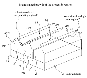
Fig.4, which is a section of a V-groove composed of facets, briefly
demonstrates a
method of the present invention. The same section continues in the direction
vertical to the
figure in Fig.4. Fig.3 is a section of a conical pit of the previous facet
growth method.
Fig.4 sections are slightly similar to Fig.3 sections. But, the actual shapes
are quite different.
CA 02543151 2002-10-O1
Don't confuse the linearly continual Fig.4 sections with the isolated Fig.3
sections. An
undersubstrate (not shown in the figures) allows a GaN crystal 22 to grow with
facets 26 in a
facet growth mode. A pair of complementarily inclining facets 26 and 26 forms
a V-groove
24. Following the bottoms (valleys) 29 of the V-grooves 24, voluminous defect
accumulating regions (I-~ 25 grow upward. Low dislocation single crystal
regions (Z) grow
under slopes of the facets 26. There are flat tops 27 outside of the facet
grooves 24. The flat top
27 is a C-plane. C-plane growth regions (Y) 28 grow under the flat C-planes
27. The valleys 29-
lead voluminous defect accumulating regions (H).
A facet 26 leads a low dislocation single crystal region (Z). A flat top 27
Ieads a C-
plane growth region (Y). The C-plane growth regions (Y), which are low
dislocation density
single crystals, have electric resistance higher than that of the low
dislocation single crystal
regions (Z). Growing facets 26 sweep dislocations of the low dislocation
single crystal
regions (Z) and the C-plane 2? growth regions (Y) inward and converge the
dislocations into
the voluminous defect accumulating regions (H). Almost all of the dislocations
centripetally
run in parallel to the C-plane toward the voluminous defect accumulating
regions (H). A
part of dislocations couple and extinguish. 'The rest of the dislocations are
arrested and
accumulated in the voluminous defect accumulating regions (H). A voluminous
defect
accumulating region (H) consists of an inner core (S) and an interface (K).
The dislocation
annihilation/accumulation place is either a sole interface (K) or a set of an
interface (K) and a
core (S). The interface (K) or the core (S) never allow once-captivated
dislocations to
escape therefrom.
Unlike a narrow defect assembly I S as shown in Fig.3( 1 ), the present
invention
prepares wide voluminous defect accumulating regions (H) and storing
dislocations by the
voluminous defect accumulating regions (H) with a definite thickness. Wideness
and
voluminousness enable the voluminous defect accumulating regions (H) to
accommodate far
21
CA 02543151 2002-10-O1
more dislocations than the lean defect assembly 15 of Fig.3(1). One advantage
of the
present invention is the vast capacity of the voluminous defect accumulating
regions (H).
Instead of polygonal pits, the present invention employ linear facets aligning
as wide
strips extending in a definite direction. Six radial corner lines, which
accompany polygonal
pits, do not occur on a surface composed of the linear facets. The linear
facets would not
make radial planar defects. The present invention can avoid the difficulty of
occurrence of
planar defects, which is a drawback of the previous facet growth, by adopting
linear facets.
It is confirmed that linear facet slopes enable linear polycrystalline regions
with grain
boundaries (K) to occur at the bottoms of the facets and the grain boundaries
(K) to act as a
dislocation annihilation/accumulation place.
The dislocation annihilation/accumulation places allow the present invention
to
eliminate the hazy dislocation diffusion from the confluence. The dislocation
annihilation/accumulation places clear stagnating dislocations away from the
narrow
confluence. The dislocation annihilation/accumulation places also kill radial
planar defects
10 as shown in Fig. l (b).
The polycrystalline regions are suitable for the annihilation/accumulation
places.
The polycrystal character allows the voluminous defect accumulating regions
(H) to
accommodate much many dislocations. The inventors found out that the effective
dislocation annihilation/accumulation place is not restricted to the
polycrystalline regions (H).
Besides polycrystalline voluminous defect accumulating regions (H), some sorts
of
single crystal regions are also effective as the dislocation
annihilation/accumulation places.
Available single crystal regions (H) are a single crystal having an
orientation slanting to the
surrounding single crystal regions, a single crystal having an interface
composed of planar
defects, and a single crystal having an interface built with small inclination
grain boundaries.
Surprisingly, another single crystal (H) having an inverse polarity, which
means the direction
22
CA 02543151 2002-10-O1
of a c-axis, is also available for a dislocation annihilation/accumulation
place.
Polycrystalline and single crystal voluminous defect accumulating regions (H)
have a large
volume with a definite width h. The large volume ensures large capacity of
storing
dislocations.
The dislocation annihilation/accumulation regions have a definite width h
instead of
an indefinitely thin regions (=planes). The definite thickness and volume of
the
annihilation/accumulation regions (H) have advantages over conventional ELO
methods. A
conventional epitaxial lateral overgrowth method (ELO) utilizing a similai
stripe structure
forms small facets, gathers dislocations by the facets to bisecting planes
between neighboring
windows, and stores the dislocations at the bisecting planes which become
planar defects. The
planar defects made by the conventional ELO have neither a sufficient
thickness nor an
enough volume, since the thickness of the planes is indefinitely small. Excess
concentration
of dislocations enhances the repulsion among dislocations, releases the
dislocations and
allows the dislocations to diffuse outward.
On the contrary, the present invention can produce the voluminous defect
accumulating region (H) having a sufficient, definite thickness. The definite
thickness
produces two interfaces on both sides. Dislocations attracted from a left side
are arrested and
stored on a left side interface KL. Dislocations attracted from a right side
are gathered and
accommodated on a right side interface KR. Dislocations are divided into
halves. The number
of the dislocations accumulated on an interface is reduced to a half. The
division weakens
mutual repulsion among converged dislocations.
The voluminous defect accumulating region (H) is a region having a definite
thickness.
Inner cores (S) can also accommodate dislocations. The dislocation density per
unit volume is
reduced by additional accumulation in the cores (S). Lower dislocation density
in the
voluminous defect accumulating regions (H) prevents dislocations from relaxing
and
23
CA 02543151 2002-10-O1
escaping.
The conventional ELO method relies upon C-plane growth which maintains a
smooth
C-plane surface without facets. The dislocations once assembled into the
planar defects
(bisecting planes) are not constricted and begin to disentangle themselves
from the planar
defects. Diffusion of the dislocations proceeds during the growth.
Dislocations disperse
uniformly in the growing GaN crystal. An average dislocation density is about
10' cm- Z in
the GaN crystal obtained by the conventional ELO. The GaN crystal of such a
10' cm- 2
high dislocation density is entirely useless for a substrate for making InGaN
laser diodes.
This invention succeeds in avoiding burying of facet slopes, in maintaining
the. facet
slopes by forming voluminous defect accumulating regions (H) of a definite
thickness, and in
captivating dislocations in the voluminous defect accumulating regions (H).
This is a feature of the present invention. What enables the regions (H) to
encapsulate
dislocations is either polycrystalline voluminous defect accumulating regions
(H) or single
crystalline voluminous defect accumulating regions (H) having shallow facets
on the top.
The defect accumulating regions (H)'should have a definite width for
permanently
arresting dislocations. The "definite width" is signified by a word
"voluminous". Thus, the
accumulating regions are called "voluminous" defect accumulating regions (H).
The gist of
the present invention is to decrease dislocations by growing GaN with
voluminous defect
accumulating regions (H). The width of the voluminous defect accumulating
regions (H) is 1
p, m to 200 p. m. Interfaces 30 exist between the voluminous defect
accumulating regions (H)
and the low dislocation single crystal regions (Z).
The voluminous defect accumulating regions (H) and the low dislocation single
crystal regions (Z) occur, satisfying a complementary relation. Controlling
positions and sizes
of voluminous defect accumulating regions (H) occurring determines positions
and sizes of
the low dislocation single crystal regions (Z). The positions and sizes of
voluminous defect
accumulating regions (H) can be predetermined by implanting mask as a seed of
growing
24
CA 02543151 2002-10-O1
voluminous defect accumulating regions (H) at an early stage of growth. The
seed makes a
voluminous defect accumulating region (H) thereupon. A set of facets having
slopes is made
in the neighborhood of the voluminous defect accumulating regions (H). The
facets induce
formation of low dislocation single crystal regions (Z) following the facets.
Thus,
implantation of the seed mask can control the sizes and positions of the low
dislocation single
crystal regions (Z) via formation of voluminous defect accumulating regions
(H).
Motivation of making facet valleys leading voluminous defect accumulating
regions
(H) depends upon the kinds of the voluminous defect accumulating regions (H).
A common
motivation is the stripe mask which produces cavities upon the stripes by
delaying growth.
Growing speed on the mask stripes is lower than the speed on the
undersubstrate. The delay
of forming surfaces is a reason of making cavities upon the stripes. The
cavities stabilize
forming and maintaining facet valleys following the stripes.
The voluminous defect accumulating regions (H) has a tendency of inviting
occurrence of milder inclining facets thereupon. The milder (shallower) facets
form stable
valleys made of facets (Fig.S(b)).
Positions of the valleys are determined. The state having valleys of facets is
stable.
The valleys are not buried but maintained. Controlling positions of facets is
realized by this
process. Therefore, positions of low dislocation single crystal regions (Z)
and defect
accumulating regions (H) are determined and controllable. The low dislocation
single
crystal regions (Z) and the defect accumulating regions (H) can be regularly
arranged. This
is one of important points in this invention.
The voluminous defect accumulating regions (H) appear in various versions.
Polycrystalline or single crystalline voluminous defect accumulating regions
(H) originate
from the mask. Polycrystalline voluminous defect accumulating regions (H)
discern
themselves from the surrounding portions by the difference of a crystalline
structure. Single
CA 02543151 2002-10-O1
crystal voluminous defect accumulating regions (H) can discriminate themselves
from the
surrounding portions by existence of interfaces. For example, a single crystal
voluminous
defect accumulating region (H) is encapsulated by interfaces of planar
defects.
The planar defect interface is induced by milder (shallower) sloped facets
appearing at
an early stage of growth on the top, and the shallow facets make the planar
defect interface as
interface between two kinds of facets. Cooperation of two different slope
facets gather
dislocations into the interfaces therebetween, which therefore become a
dislocation
annihilation/accumulatiort place.
A conspicuous, unexpected feature is frequently appearing polarity-inversion
of
voluminous defect accumulating regions (H). The polarity (direction of c-axis)
of the
voluminous defect accumulating regions (H) is different by 180 degrees from
the c-axis of the
other low dislocation single crystal regions (Z) and C-plane growth regions
(Y). In the
inversion case, clear grain boundaries happen at the interfaces between the
voluminous defect
accumulating regions (H) and the low dislocation single crystal regions (Z).
The interface
grain boundaries play an active role of accumulating the dislocations swept
and gathered by
the growing facets. In particular in the case of the polarity-inversion
occurring in the
voluminous defect accumulating regions (H), controlling of the facet growth
can be
successfully achieved. The reason is that the region of the polarity-inversion
grows more
slowly than other regions, the inventors suppose.
The above is the basic principle basing the present invention.
The present invention allows a GaN crystal to solve three mentioned serious
problems;
the hazy dispersion of diffusing dislocations, the planar defects occurring at
the dislocation
confluence, and the difficulty of controlling positions of the dislocation
confluence. The
present invention grows a rack-roof GaN crystal having parallel valleys and
hills as shown in
Fig.7 and makes a flat, smooth GaN substrate of low dislocation density as
shown in Fig.B. by
26
CA 02543151 2002-10-O1
r
mechanical processing the rack-roof GaN crystal.
In Fig.7, a GaN crystal 22 grown on an undersubstrate 21 has a rack-shaped
roof of
repetitions of parallel hills and valleys which are steep facets. A voluminous
defect
accumulating region (H) accompanies a valley of the rack-roof in the vertical
direction.
Slopes forming the hills and valleys are facets 26. What accompanies the
facets 26 in the
vertical direction are the low dislocation single crystal regions (Z). Fig.7
shows a GaN crystal
having sharp ridges on the hills without flat C-plane growth regions (Y). In
this case, the
pad held between neighboring voluminous defect accumulating regions (H) is a
uniform low
dislocation single crystal region (Z). The pitch p, the widths z and h satisfy
an equation p=z+h.
Otherwise in the case of a GaN including C-plane growth regions (Y), the pitch
p, the widths
z, y and h satisfy another equation p=2z+y+h. The relation between the height
of the hill and
the pitch p is described later. Fig.8 demonstrates a rectangle wafer made by
eliminating the
undersubstrate from the as-grown GaN substrate, grinding the rack-roof on the
top surface
and polishing both surfaces of the ground wafer. The GaN wafer has a HZYZHZYZH
structure having regularly, periodically aligning voluminous defect
accumulating regions (H),
low dislocation single crystal regions (Z) and C-plane growth regions (Y). The
shape of
the C-plane growth regions (Y) depends upon the growth condition. Sometimes
the C-plane
growth regions (Y) meander with a fluctuating width.
According to an aspect of the invention there is provided a GaN substrate
having
a top surface and a bottom surface, the top surface comprising a linear low
dislocation
single crystal region (Z) having a width of 10 ,u m to 2000 ~ m and extending
in a
direction defined on the top surface, and two linear defect accumulating
regions (H)
having a width of 1 ,u m to 200 ,u m and extending in the same direction as
the low
dislocation single crystal region (Z), having interfaces (K) on both sides and
being in
contact with the low dislocation single crystal regions (Z) via the interfaces
(K).
27
CA 02543151 2002-10-O1
According to another aspect of the invention there is provided a GaN substrate
having a top surface and a bottom surface, the top surface comprising
repetitions
(ZHZHw) of a unit (ZH) having a pair of a linear low dislocation single
crystal region
(Z) having a width of 10 ,u m to 2000 ,u m and extending in a direction
defined on the top
surface and a linear defect accumulating region (H) having a width of I ~ m to
200 ,u m
and extending in the same direction as the low dislocation single crystal
region (Z),
having interfaces (K) on both sides and being in contact with the low
dislocation single
crystal region (Z) via the interfaces (K).
According to a further aspect of the invention there is provided a GaN
substrate
having a top surface, a bottom surface and a definite thickness, the GaN
substrate
comprising a planar low dislocation single crystal region (Z) having a width
of 10 ,u m to
2000 ,u m and extending in both a direction of thickness and a direction
defined on the
top surface, and two planar voluminous defect accumulating regions (H) having
a width
of I ~ m to 200 ~ m and extending in the same directions as the low
dislocation single
I S crystal region (Z), having interfaces (K) on both sides and being in
contact with the low
dislocation single crystal regions (Z) via the interfaces (K).
According to a further aspect of the invention there is provided a GaN
substrate
having a top surface, a bottom surface and a definite thickness, the GaN
substrate
comprising repetitions (ZHZHw) of a unit (ZH) having a pair of a planar low
dislocation
single crystal region (Z) having a width of I O ,u m to 2000 ,u m and
extending both in a
direction of thickness and in a direction defined on the top surface and a
planar
voluminous defect accumulating region (H) having a width of I ,u m to 200 ~ m
and
extending in the same directions as the low dislocation single crystal region
(Z), having
interfaces (K) on both sides and being in contact with the low dislocation
single crystal
region (Z) via the interfaces (K).
According to a further aspect of the invention there is provided a GaN
substrate
having a top surface and a bottom surface, the top surface comprising parallel
planar
defect accumulating regions (H) accumulating dislocations, having a width of 1
,u m to
200 ,u m and aligning periodically, regularly with a pitch p, and parallel
planar low
27a
CA 02543151 2002-10-O1
dislocation single crystal regions (Z) having a width of 10 ,u m to 2000 ,u m
and being
sandwiched between the neighboring planar defect accumulating regions (H) or a
set
(ZYZ) of parallel planar low dislocation single crystal regions (Z) and a C-
plane growth
region (Y) with higher resistivity than other regions between the neighboring
planar
defect accumulating regions (H).
According to a further aspect of the invention there is provided a method of
growing GaN comprising the steps of preparing an undersubstrate, forming a
mask
having parallel, linear stripes on the undersubstrate, preparing parallel
masked parts and
parallel exposed parts on the undersubstrate, growing a set (HZH) of a linear
low
dislocation single crystal region (Z) having a width of 10 ,u m to 2000 ,u m
on the
exposed parts and two linear voluminous defect accumulating regions (H) having
a width
of 1 ~. m to 200 ~ m on the masked parts including plenty of dislocations and
being in
contact with the low dislocation single cxystal region (Z) on the
undersubstrate, attracting
dislocations existing in the low dislocation single crystal region (Z) to the
voluminous
defect accumulating regions (H), making use of cores (S) or interfaces (K) of
the
voluminous defect accumulating regions (H) as an annihilationJaccumulation
place of
dislocations, and reducing dislocations in the low dislocation single crystal
region (Z).
According to a further aspect of the invention there is provided a method of
growing GaN comprising the steps of preparing an undersubstrate, forming a
mask
having parallel, linear stripes on the undersubstrate, preparing parallel
masked parts and
parallel exposed parts on the undersubstrate, growing a set (HZYZH) of a
linear C-plane
growth region (Y), two linear low dislocation single crystal regions (Z)
having a width of
10 ~ m to 2000 ~ m on the exposed parts neighboring to the C-plane growth
region (Y),
two linear voluminous defect accumulating regions (H) having a width of 1 ,u m
to 200 p
m on the masked parts including plenty of dislocations and being in contact
with the low
dislocation single crystal regions (Z) on the undersubstrate, attracting
dislocations
existing in the low dislocation single crystal regions (Z) and the C-plane
growth region
(Y) to the voluminous defect accumulating regions (H), making use of cores (S)
or
interfaces (K) of the voluminous defect accumulating regions (H) as an
27b
CA 02543151 2002-10-O1
annihilation/accumulation place of dislocations, and reducing dislocations in
the low
dislocation single crystal regions (Z) and the C-plane growth region (Y).
According to a further aspect of the invention there is provided a method of
growing GaN comprising the steps of preparing an undersubstrate, forming a
mask
having parallel, linear stripes on the undersubstrate, preparing parallel
masked parts and
parallel exposed parts on the undersubstrate, growing a GaN crystal on the
undersubstrate, making linearly extending, reciprocally slanting facets
forming valleys
and a hill, growing a set (HZH) composed of a linear low dislocation single
crystal region
(Z) having a width of 10 ~ m to 2000 ~ m on the exposed parts and two linear
I O voluminous defect accumulating regions (H) having a width of 1 ,u m to 200
~c m on the
masked parts, the linear low dislocation single crystal region (Z) dangling
from two
reciprocally slanting facets, the linear voluminous defect accumulating
regions (H)
hanging from the valleys and sandwiching the low dislocation single crystal
region (Z),
maintaining the facets, the valleys and the hill, attracting dislocations in
the low
dislocation single crystal region (Z) into the voluminous defect accumulating
regions (H)
by growing the facets, making use of cores (S) or interfaces (K) of the
voluminous defect
accumulating regions (H) as an annihilation/accumulation place of
dislocations, and
reducing dislocations in the low dislocation single crystal region (Z).
According to a further aspect of the invention there is provided a method of
growing GaN comprising the steps of preparing an undersubstrate, forming a
mask
having parallel, linear stripes on the undersubstrate, preparing parallel
masked parts and
parallel exposed parts on the undersubstrate, growing a GaN crystal on the
undersubstrate, making linearly extending, slanting facets forming a valley
and hills,
growing a set (ZHZ) composed of a linear voluminous defect accumulating region
(H)
having a width of 1 ~ m to 200 ,u m on the masked parts and two linear low
dislocation
single crystal regions (Z) having a width of 10 ~ m to 2000 ,u m on the
exposed parts, the
linear voluminous defect accumulating region (H) dangling from the valley of
the facets, the
linear low dislocation single crystal regions (Z) hanging from the facets and
sandwiching the
voluminous defect accumulating region (H), maintaining the facets, the valley
and the
27c
CA 02543151 2002-10-O1
hills, attracting dislocations in the low dislocation single crystal regions
(Z) into the
voluminous defect accumulating region (H) by growing the facets, making use of
cores
(S) or interfaces (K) of the voluminous defect accumulating region (H) as an
annihilation/accumulation place of dislocations, and reducing dislocations in
the low
dislocation single crystal regions (Z).
According to a further aspect of the invention there is provided a method of
growing GaN comprising the steps of preparing an undersubstrate, forming a
mask
having parallel, linear stripes on the undersubstrate, preparing parallel
masked parts and
parallel exposed parts on the undersubstrate, growing a GaN crystal on the
undersubstrate, making linearly extending, reciprocally slanting facets
forming valleys
and hills, growing regularly and periodically aligning parallel units (HZ)
composed of a
linear voluminous defect accumulating region (H) having a width of 1 ~ m to
200 ,u m on
the masked parts and a linear low dislocation single crystal region (Z) having
a width of
10 ~ m to 2000 ~ m on the exposed parts being in contact with the voluminous
defect
accumulating region (H), the linear low dislocation single crystal regions (Z)
hanging
from two reciprocally slanting facets and sandwiching the voluminous defect
accumulating regions (H), maintaining the facets, the valleys and the hills,
attracting
dislocations in the low dislocation single crystal regions (Z) into the
voluminous defect
accumulating regions (H) by growing the facets, making use of cores (S) or
interfaces
(K) of the voluminous defect accumulating regions (H) as an
annihilation/accumulation
place of dislocations, reducing dislocations in the low dislocation single
crystal regions
(Z), and obtaining a HZHZHZ structure constructed by repetitions of the (HZ)
units.
According to a further aspect of the invention there is provided a method of
growing GaN comprising the steps of preparing an undersubstrate, forming a
mask
having parallel, linear stripes on the undersubstrate, preparing parallel
masked parts and
parallel exposed parts on the undersubstrate, growing a GaN crystal on the
undersubstrate, making linearly extending, slanting facets forming valleys and
hills,
growing regularly and periodically aligning parallel units (HZ) composed of a
linear
voluminous defect accumulating region (H) having a width of 1 ~ m to 200 p m
on the
27d
CA 02543151 2002-10-O1
F
masked parts and a linear low dislocation single crystal region (Z) having a
width of 10 ~
m to 2000 ,u m on the exposed parts being in contact with the voluminous
defect
accumulating region (H), the linear voluminous defect accumulating regions (H)
dangling from the valleys of the facets, the linear low dislocation single
crystal regions
(Z) hanging from the facets and sandwiching the voluminous defect accumulating
regions (H), maintaining the facets, the valleys and the hills, attracting
dislocations in the
low dislocation single crystal regions (Z) into the voluminous defect
accumulating
regions (H) by growing the facets, making use of cores (S) or interfaces (K)
of the
voluminous defect accumulating regions (H) as an annihilation/accumulation
place of
dislocations, reducing dislocations in the low dislocation single crystal
regions (Z), and
obtaining a HZHZHZw structure constructed by repetitions of the (HZ) units.
According to a further aspect of the invention there is provided a method of
growing GaN comprising the steps of preparing an undersubstrate, forming a
mask
having parallel, linear stripes on the undersubstrate, preparing parallel
masked parts and
1 S parallel exposed parts on the undersubstrate, growing a GaN crystal on the
undersubstrate, making linearly extending, slanting facets forming valleys and
hills,
growing regularly and periodically aligning parallel units (HZYZ) composed of
a linear
voluminous defect accumulating region (H) on the masked parts, a linear low
dislocation
single crystal region (Z) on the exposed parts, a C-plane growth region (Y)
and another
low dislocation single crystal region (Z) which are piled in this series, the
linear
voluminous defect accumulating regions (H) dangling from the valleys of the
facets, the
linear low dislocation single crystal regions (Z) hanging from the facets and
sandwiching
the voluminous defect accumulating regions (H), the C-plane growth regions (Y)
having
a flat top surface with high electric resistivity, maintaining the facets, the
valleys and the
hills, attracting dislocations in the low dislocation single crystal regions
(Z) and the C-
plane growth regions (Y) into the voluminous defect accumulating regions (H)
by
growing the facets, making use of cores (S) or interfaces (K) of the
voluminous defect
accumulating regions (H) as an annihilation/accumulation place of
dislocations, reducing
dislocations in the low dislocation single crystal regions (Z) and the C-plane
growth
27e
CA 02543151 2002-10-O1
regions (Y), and obtaining a HZYZHZYZHw- structure constructed by repetitions
of the
(HZYZ) units.
According to a further aspect of the invention there is provided a method of
growing GaN comprising the steps of preparing an undersubstrate, forming a
mask
having parallel, linear stripes with a pitch p regularly on the
undersubstrate, preparing
parallel masked parts and parallel exposed pans on the undersubstrate, growing
linear
low dislocation single crystals regions (Z) with a width of 10 ~ m to 2000 ~t
m on the
exposed parts and linear voluminous defect accumulating regions (H) with a
width of 1 ,u
m to 200 ,u m on the masked parts, aligning parallel linear voluminous defect
accumulating regions (H) with a pitch p regularly on an undersubstrate, and
allotting a
linear low dislocation single crystal region (Z) or a set of a linear low
dislocation single
crystal region (Z), a C-plane growth region (Y) and another linear low
dislocation single
crystal region (Z) between every neighboring voluminous defect accumulating
regions
(H).
According to a further aspect of the invention there is provided a method of
growing GaN comprising the steps of preparing an undersubstrate, forming a
mask
having parallel, linear stripes with a pitch p regularly on the
undersubstrate, preparing
parallel masked parts and parallel exposed parts on the undersubstrate,
preparing a mask
having a plurality of parallel linear stripes on an undersubstrate, growing a
GaN crystal
on the undersubstrate with the mask, growing linear low dislocation single
crystal regions
(Z) with a width of 10 ,u m to 2000 ~ m on the exposed parts and linear
voluminous
defect accumulating regions (H) with a width of 1 ,u m to 200 ~c m on the
masked parts,
forming a plurality of parallel linear voluminous defect accumulating regions
(H) having
a width of 1 ~ m to 200 ,u m on the stripes of the mask, and forming low
dislocation
single crystal regions (Z) having a width of I 0 ~ m to 2000 ~u m or low
dislocation single
crystal regions (Z) and C-plane growth regions (Y) on other parts except the
linear stripes
of the undersubstrate.
According to a further aspect of the invention there is provided a method of
producing a GaN substrate comprising the steps of preparing an undersubstrate,
forming
27f
CA 02543151 2002-10-O1
a mask having parallel, linear stripes with a pitch p regularly on the
undersubstrate,
preparing parallel masked pans and parallel exposed parts on the
undersubstrate, growing
a GaN crystal on a facet-growth condition, growing linear low dislocation
single crystals
regions (Z) with a width of 10 ,u m to 2000 ,u m on the exposed parts and
linear
voluminous defect accumulating regions (H) with a width of 1 ,u m to 200 ,u m
on the
masked parts, making voluminous defect accumulating regions (H), reducing
dislocations
in low dislocation single crystal regions (Z) having a width of 10 ,u m to
2000 ,u m and C-
plane growth regions (Y) in contact with the voluminous defect accumulating
regions (H)
by utilizing interfaces (K) and cores (S) of the voluminous defect
accumulating regions
(H) as dislocation annihilation/accumulation places, obtaining a rack-shaped
as-grown
GaN crystal, mechanical-processing the as-grown GaN crystal, and making a
flat, smooth
single crystal GaN substrate.
According to a further aspect of the invention there is provided a method of
producing a GaN substrate comprising the steps of preparing an undersubstrate,
forming
a mask having parallel, linear stripes with a pitch p regularly on the
undersubstrate,
preparing parallel masked parts and parallel exposed parts on the
undersubstrate, growing
a GaN crystal on a facet-growth condition, growing linear low dislocation
single crystals
regions (Z) with a width of 10 ,u m to 2000 ~t m on the exposed parts and
linear
voluminous defect accumulating regions (H) with a width of 1 ,u m to 200 ,u m
on the
masked parts, forming valleys composed of facets on a GaN growing surface;
making
voluminous defect accumulating regions (H) having a width of 1 ~c m to 200 ,u
m and
hanging from bottoms of the valleys, low dislocation single crystal regions
(Z) having a
width of 10 ,u m to 2000 ~ m under the facets and C-plane growth regions (Y)
under flat
tops of a C-plane, reducing dislocations in the low dislocation single crystal
regions (Z)
and the C-plane growth regions (Y), obtaining a rack-shaped as-grown GaN
crystal,
mechanical-processing the as-grown GaN crystal, and making a flat, smooth
single
crystal GaN substrate.
According to a further aspect of the invention there is provided a method of
producing a GaN substrate comprising the steps of preparing a foreign material
27g
CA 02543151 2002-10-O1
r
undersubstrate, forming a mask having parallel, linear stripes with a pitch p
regularly on
the foreign material undersubstrate, preparing parallel masked parts and
parallel exposed
parts on the undersubstrate, growing a GaN crystal on a facet-growth
condition, growing
linear low dislocation single crystal regions (Z) with a width of 10 ~ m to
2000 ~c m on
the exposed parts and linear voluminous defect accumulating regions (H) with a
width of
1 ~r m to 200 ,u m on the masked parts, forming a striped mask with parallel
stripes on a
foreign material undersubstrate, growing a GaN crystal upon the masked foreign
material
undersubstrate, forming ribbon-shaped slanting facets linearly extending in
parallel with
the stripes, making facet hills and facet valleys which coincide with the
stripes,
producing voluminous defect accumulating regions (H) having a width of 1 ,u m
to 200,u
m under the valleys of facets above the stripes, yielding low dislocation
single crystal
regions (Z) having a width of 10 ,u m to 2000 ,u m under the facets, making C-
plane
growth regions (Y) under flat tops between neighboring reciprocal facets,
maintaining the
facets, the voluminous defect accumulating regions (H), the low dislocation
single crystal
regions (Z) and the C-plane growth regions (Y), attracting dislocations from
the low
dislocation single crystal regions (Z) and the C-plane growth regions (Y) into
the
voluminous defect accumulating regions (H), annihilating and accumulating the
dislocations at the voluminous defect accumulating regions (H), reducing
dislocations in
the low dislocation single crystal regions (Z) and the C-plane growth regions
(Y), making
a thick tall GaN single crystal ingot, slicing the tall GaN single crystal
into a plurality of
as-cut wafers, and polishing the as-cut wafers into GaN mirror wafers.
According to a further aspect of the invention there is provided a method of
producing a GaN substrate comprising the steps of preparing an undersubstrate,
forming
a mask having parallel, linear stripes on the undersubstrate, preparing
parallel masked
parts and parallel exposed parts on the undersubstrate, forming a stripe mask
with parallel
stripes upon the undersubstrate, growing a GaN crystal on the undersubstrate,
making
pairs of reciprocally slanting facets linearly extending in parallel to the
mask stripes,
forming hills composed of the reciprocally slanting facets, forming valleys
composed of
the reciprocally slanting facets just above the stripes, producing voluminous
defect
27h
CA 02543151 2002-10-O1
t
accumulating regions (H) having a width of I ,u m to 200 ~r m under the
valleys above the
stripes, forming low dislocation single crystal regions (Z) having a width of
10 ~ m to
2000 ,u m under the facets above parts not covered with the stripes of the
undersubstrate,
making C-plane growth regions (Y) under flat tops between neighboring
reciprocal
facets, growing .a set (HZH) or a set (HZYZH) composed of the linear low
dislocation
single crystal region (Z) on the exposed parts, the linear voluminous defect
accumulating
region (H) on the masked parts and the C-plane growth region (Y), maintaining
the
facets, the valleys and the hills, attracting dislocations in the low
dislocation single
crystal regions (Z) and the C-plane growth regions (Y) into the voluminous
defect
accumulating regions (H) by growing the facets, making use of cores (S) or
interfaces
(K) of the voluminous defect accumulating regions (H) as an
annihilation/accumulation
place of dislocations, reducing dislocations in the low dislocation single
crystal regions
(Z), obtaining a single crystal GaN substrate with an inherent structure of
"wHZYZHZYZHw" or "wHZHZHZw", employing the GaN substrate with the inherent
I S structure of "wHZYZHZYZHw" or "wHZHZHZw" made by former steps as a seed
parent undersubstrate without mask, growing a GaN crystal upon the maskless
GaN
parent undersubstrate, forming ribbon-shaped slanting facets linearly
extending in
parallel to parent voluminous defect accumulating regions (H) of the GaN
substrate,
making facet hills and facet valleys which coincide with the inherent
voluminous defect
accumulating regions (H) of the parent GaN undersubstrate, producing
voluminous
defect accumulating regions (H) under the valleys of facets above the parent
voluminous
defect accumulating regions (H), yielding low dislocation single crystal
regions (Z) under
the facets, making C-plane growth regions (Y) at flat tops between neighboring
reciprocal facets, maintaining the facets, the voluminous defect accumulating
regions
(H), the low dislocation single crystal regions (Z) and the C-plane growth
regions (Y),
attracting dislocations from the low dislocation single crystal regions (Z)
and the C-plane
growth regions (Y) into the voluminous defect accumulating regions (H),
annihilating
and accumulating the dislocations in the voluminous defect accumulating
regions (H),
reducing dislocations in low dislocation single crystal regions (Z) and the C-
plane growth
27i
CA 02543151 2002-10-O1
r
regions (Y), making a thick tall GaN single crystal ingot, slicing the tall
GaN single
crystal ingot into a plurality of as-cut wafers, and polishing the as-cut
wafers into GaN
mirror wafers.
According to a further aspect of the invention there is provided a method of
S producing a GaN substrate comprising the steps of preparing an
undersubstrate, forming
a mask having parallel, linear stripes on the undersubstrate, preparing
parallel masked
parts and parallel exposed parts on the undersubstrate, forming a stripe mask
with parallel
stripes upon the undersubstrate, growing a GaN crystal on the undersubstrate,
making
pairs of reciprocally slanting facets linearly extending in parallel to the
mask stripes,
forming hills composed of the reciprocally slanting facets, forming valleys
composed of
the reciprocally slanting facets just above the stripes, producing voluminous
defect
accumulating regions (H) having a width of 1 ~ m to 200 ~ m under the valleys
above the
stripes, forming low dislocation single crystal regions (Z) having a width of
10 ,u m to
2000 ,u m under the facets above pans not covered with the stripes of the
undersubstrate,
making C=plane growth regions (Y) under flat tops between neighboring
reciprocal
facets, growing a set (HZH) or a set (HZYZH) composed of the linear low
dislocation
single crystal region (Z) on the exposed parts, the linear voluminous defect
accumulating
region (H) on the masked parts and the C-plane growth region (Y), maintaining
the
facets, the valleys and the hill, attracting dislocations in the low
dislocation single crystal
regions (Z) and the C-plane growth regions (Y) into the voluminous defect
accumulating
regions (H) by growing the facets, making use of cores (S) or interfaces (K)
of the
voluminous defect accumulating regions (H) as an annihilation/accumulation
place of
dislocations, reducing dislocations in the low dislocation single crystal
regions (Z) and
the C-plane growth regions (Y), obtaining a single crystal GaN substrate with
an inherent
structure of "-wHZYZHZYZHw-" or "wHZHZHZ---", employing the GaN substrate with
the inherent structure of "wHZYZHZYZHw" or "wHZHZHZw" made by former steps
as a seed parent undersubstrate without mask, growing a GaN crystal upon the
maskless
GaN undersubstrate, forming ribbon-shaped slanting facets linearly extending
in parallel
with the parent voluminous defect accumulating regions (H) of the GaN
substrate,
27j
CA 02543151 2002-10-O1
making facet hills and facet valleys which coincide with the inherent
voluminous defect
accumulating regions (H) of the parent GaN undersubstrate, forming less
inclining
shallow facets just on the valleys, producing voluminous defect accumulating
regions (H)
under the valley shallow facets above the parent voluminous defect
accumulating regions
(H), yielding low dislocation single crystal regions (Z) or C-plane growth
regions (Y)
s upon the parent inherent low dislocation single crystal regions (Z) and the
parent C-plane
growth regions (Y), maintaining the facets, the voluminous defect accumulating
regions
(H), the low dislocation single crystal regions (Z) and the C-plane growth
regions (Y),
attracting dislocations from the low dislocation single crystal regions (Z)
and the C-plane
growth regions (Y) into the voluminous defect accumulating regions (H),
annihilating
and accumulating the dislocations in the voluminous defect accumulating
regions (H),
to reducing dislocations in the low dislocation single crystal regions (Z) and
the C-plane
growth regions (Y), making a thick tall GaN single crystal ingot, slicing the
tall GaN
single crystal into a plurality of as-cut wafers, and polishing the as-cut
wafers into GaN
mirror wafers.
According to an aspect of the invention there is provided a GaN substrate
having
15 a top surface, a bottom surface, a thickness, planar low dislocation single
crystal regions
having a width of 10 ~m to 2000 pm, linearly extending in a direction parallel
to the top
and bottom surfaces and piercing from the top surface to the bottom surface,
and
voluminous defect accumulating regions having a width of 1 ~m to 200 pm,
linearly
extending in the direction parallel to the low dislocation single crystal
regions and
2o piercing from the top surface to the bottom surface accompanied by
boundaries on both
sides, the voluminous defect accumulating regions being in contact via the
boundaries
with the low dislocation single crystal regions wherein the low dislocation
single crystal
regions have voluminous C-growth regions at the middles, and widths of the
voluminous
C-growth regions are not constant but are fluctuating in both the direction of
the
2s thickness and the planar direction of the low dislocation single crystal
region.
27k
CA 02543151 2002-10-O1
According to another aspect of the invention there is provided a method of
growing GaN comprising the steps of preparing an undersubstrate with surfaces,
growing
repetitions of a set consisting of two voluminous low dislocation single
crystal regions
having a width of 10 ~.m to 2000 ~.m and extending in a direction of thickness
and in a
planar direction parallel to the surfaces, voluminous C-plane growth regions
sandwiched
by the two low dislocation single crystal regions and voluminous defect
accumulating
regions having a width of 1 p.m to 200 ~tm and having boundaries, the
voluminous defect
accumulating region being in parallel and in contact with the voluminous low
single
to crystal regions via the boundaries wherein widths of the C-plane growth
regions are
fluctuating in both the direction of the thickness and the planar direction of
the
voluminous low dislocation single crystal regions.
According to a further aspect of the invention there is provided a method of
15 growing GaN comprising the steps of preparing an undersubstrate with
surfaces, growing
repetitions of a set of consisting of a voluminous low dislocation single
crystal region
having a width of 10 ~m to 2000 ~m and extending in a direction of thickness
and in a
planar direction parallel to the surfaces, and a voluminous defect
accumulating region
having a width of 1 ~,m to 200 ~m and having boundaries and a core, the
voluminous
2o defect accumulating region being in parallel and in contact with the
voluminous low
single crystal regions via the boundaries wherein the set makes facets having
bottoms at
the voluminous defect accumulating region and maintains the facets till the
end of the
crystal growth, the facets attract dislocations existing in neighboring
regions to the facet
bottoms and the core or the boundaries of the defect accumulating regions,
play a role of
271
CA 02543151 2002-10-O1
accumulating and extinguishing the dislocations and reduce the dislocations in
the
neighboring low dislocation single crystal regions.
To achieve the foregoing objects and in accordance with the purpose of the
invention,
S embodiments will be broadly described herein.
The present invention succeeds in obtaining a low dislocation density GaN
single
crystal substrate by making parallel facet V-grooves by the facet growth,
producing
voluminous defect accumulating regions (H) at the valleys , depriving other
parts of
dislocations by the facets, gathering dislocations to the voluminous defect
accumulating
regions (H) at the valleys (bottoms) of the V-grooves and
annihilating/accumulating the
27m
CA 02543151 2002-10-O1
dislocations in the voluminous defect accumulating regions (H) permanently.
The formation
of the voluminous defect accumulating regions (H) enable the present invention
to solve all
the three problems aforementioned;
(1) to reduce the hazy dislocation diffusion dispersing from the defect
assemblies below the
valleys of facets;
(2) to extinguish the planar defects formed below the valleys of facets; and
(3) to control the positions of the defect assemblies formed under the valleys
of the facets.
The present invention can make a low dislocation density GaN single crystal
substrate
by controlling the positions of the voluminous defect accumulating regions
(H). The major
portions (Z) and (Y) of the GaN substrate of the present invention are low
dislocation density
single crystals obtained by concentrating dislocations into narrow, restricted
portions aligning
regularly and periodically. The GaN substrates are suitable for a low
dislocation substrate for
fabricating blue, violet light laser diodes.
In the accompanying drawings:
Fig.l are perspective views of a pit composed of facets which have been
produced by
a facet growth method, which was proposed in the previous Japanese Patent
Laying Open
No.2001-102307 invented by the inventors of the present invention, for growing
a GaN
crystal with maintaining facets on a growing surface, and for clarifying that
facets grow
slantingly inward and gather dislocations to corner lines. Fig.l (a) exhibits
that dislocations
are swept inward by growing inclining facets and are stored at the bottom of
the pit. Fig. l (b)
shows that mutual repulsion causes six radial planar defects hanging from the
corner lines.
Fig.2 is a plan view of a pit for showing that dislocations are swept and
gathered to
corner lines by inward growing facets and accumulated at dislocation
confluence (manifold
point) under the center bottom of the pit in a facet growth suggested by
Japanese Patent
Laying Open No.2001-102307 invented by the inventors of the present invention.
28
CA 02543151 2002-10-O1
Fig.3 are vertically sectioned views of a pit for showing that dislocations
are swept
and gathered to the corner lines by inward growing facets and accumulated at
dislocation
confluence (manifold point) under the center bottom of the pit and shaped into
longitudinally
extending bundles of dislocations hanging from the bottom in a facet growth
suggested by
Japanese Patent Laying Open No.2001-102307 invented by the inventors of the
present
invention. Fig.3(1) demonstrates a bundle of dislocations which are formed
wish
dislocations gathered by the facet growth. Fig.3(2) demonstrates that the
dislocation bundle is
not closed but open and strong repulsion releases the once gathered
dislocations outward into
hazy dislocation dispersion.
Fig.4 are vertically sectioned views of a longitudinally extending V-groove
having a
valley for showing that dislocations are transferred by inward growing facets
and are formed
into voluminous defect accumulating regions (H) dangling from the valley of
the facets.
Fig.4(1) indicates that the facet growth concentrates dislocations to the
voluminous defect
accumulating region (H) at the bottom of the valley. Fig. 4(~) shows the
voluminous defect
accumulating region (H) at the bottom absorb dislocations by the upward
growth.
Fig. S are sectional views of a sample at various steps for demonstrating the
steps of
the present invention of making a linearly extending stripe mask 23 on an
undersubstrate 21,
growing a GaN crystal 22 on the masked undersubstrate 21, producing linear
facets 26 on the
stripe mask 23, producing voluminous defect accumulating regions (H) 25 under
the valleys
29 of the facets 26, and growing low dislocation single crystal regions (Z)
neighbouring the
voluminous defect accumulating regions (H) 25. Fig. 5(a) shows a single facet
case having
sets of steep slope facets without shallow facets. Fig. 5(b) shows a double
facet case having
sets of steep slope facets followed by sets of shallow facets.
Fig.6 are CL plan views of a stripe mask and a grown GaN crystal for showing a
GaN growth of the present invention. Fig.6(a) is a CL plan view of a sample
having a stripe
29
CA 02543151 2002-10-O1
mask on an undersubstrate. Fig.6(b) is 'a ' CL plan view of a GaN crystal
having a
ZHZYZHZYZ-wstructure of repetitions of a set of a voluminous defect
accumulating region
(H), a low dislocation single crystal region (Z) and a C-plane growth region
(Y).
Fig.7 is an oblique view of a rack-shaped as-grown GaN crystal having a ZHZHZw
periodic structure of repetitions of a set of a voluminous defect accumulating
region (H) and a
low dislocation single crystal region (Z) which are made by forming a stripe
mask on an
undersubstrate and growing a GaN crystal epitaxially on the masked
undersubstrate.
Fig.8 is a perspective CL view of a mirror polished GaN crystal having a
ZHZYZHZYZ~ ~ periodic structure of repetitions of a set of a voluminous defect
accumulating
region (H), a low dislocation single crystal region (Z) and a C-plane growth
region (Y) which
are made by forming a stripe mask on an undersubstrate and growing a GaN
crystal
epitaxially on the masked undersubstrate.
Fig.9 are CL plan views of mirror polished GaN crystals having a ZHZYZHZYZ~ ~'
periodic structure of repetitions of a set of a voluminous defect accumulating
region (H), low
dislocation single crystal region (Z) and a C-plane growth region (Y) which
are made by
forming a stripe mask on an undersubstrate and growing a GaN crystal
epitaxially on the
masked undersubstrate. Fig.9(a) is the CL plan view of the minor polished GaN
crystal
having a ZHZYZHZYZ~ ~ periodic structure which is made by forming a stripe
mask in
parallel to a <1-100> direction of GaN on an undersubstrate and growing a GaN
crystal
epitaxially on the masked undersubstrate. Fig.9(b) is the CL plan view of the
mirror
polished GaN crystal having a ZHZYZHZYZ~ ~ periodic structure which is made by
forming a
stripe mask in parallel to a <11-20> direction of GaN on an undersubstrate and
growing a
GaN crystal epitaxially on the masked undersubstrate.
Fig.lO are sectional views of a sample at various steps for demonstrating the
steps of
the present invention of making a linearly extending stripe mask on an
undersubstrate,
CA 02543151 2002-10-O1
growing a GaN crystal on the masked undersubstrate; producing linear facets on
the stripe
mask, producing voluminous defect accumulating regions (H) under valleys of
the facets and
growing low dislocation single crystal regions (Z) neighboring the voluminous
defect
accumulating regions (H), grinding a rugged faceted surface, eliminating the
undersubstrate
for separating a GaN substrate, and lapping the GaN substrate and polishing
the GaN
substrate. Fig.lO(1) shows a sapphire undersubstrate. Fig.lO(2) denotes a
sample having a
GaN epi-layer formed on the sapphire undersubstrate. Fig. 10(3) illustrates a
stripe mask
formed on the GaN epi-layer. Fig.lO(4) shows a CL section of an as-grown GaN
sample
having a facet surface with valleys, voluminous defect accumulating regions
(H) following
the valleys, low dislocation single crystal regions (Z) under the facets and C-
plane growth
regions (Y) under the flat tops. Fig.lO(5) shows a section of a mirror
polished GaN substrate
having a HZYZHZYZH---structure composed of the voluminous defect accumulating
regions
(H), low dislocation single crystal regions (Z) and the C-plane growth regions
(Y).
Fig.l l are sectional views of a sample at various steps for demonstrating the
steps of
the present invention of making a linearly extending stripe mask on an
undersubstrafe,
growing a GaN crystal on the masked undersubstrate, producing linear facets on
the stripe
mask, producing voluminous defect accumulating regions (H) under valleys of
the facets and
growing low dislocation single crystal regions (Z) neighboring the voluminous
defect
accumulating regions (H), grinding a rugged faceted surface, eliminating the
undersubstrate
for separating a GaN substrate, and lapping the GaN substrate and polishing
the GaN
substrate. Fig.ll(1) shows a foreign material undersubstrate with a stripe
mask. Fig.ll(2)
denotes a CL section of an as-grown GaN sample having a facet surface with
valleys,
voluminous defect accumulating regions (H) following the valleys, low
dislocation single
crystal regions (Z) under the facets and C-plane growth regions (Y) under the
flat tops.
Fig.ll(3) shows a section of a mirror polished GaN substrate having a
HZYZHZYZHw
31
CA 02543151 2002-10-O1
structure composed of the voluminous defect accumulating regions (H), low
dislocation single
crystal regions (Z) and the C-plane growth regions (Y).
Fig. 12 is a series of sectional views of steps of making a GaN crystal
Embodiment 4
of the present invention by preparing a GaN seed substrate made by the former
embodiments
of the present invention, growing a thick GaN epitaxial crystal on the seed
GaN substrate on
the condition of facet growing, forming linearly extending slanting facets and
linearly
extending facet hills on parent low dislocation single crystal regions (Z) and
parent C-plane
growth regions (Y) of the GaN seed substrate, forming facet valleys just upon
parent
voluminous defect accumulating regions (H) of the GaN seed, producing
voluminous defect
accumulating regions (H) under the bottoms of the valleys on the parent
voluminous defect
accumulating regions (H), forming low dislocation single crystal regions (Z)
and C-plane
growth regions (Y) under the hills and the facets on the parent low
dislocation single crystal
regions (Z) and the parent C-plane growth regions (Y), slicing an as-grown
thick crystal into a
plurality of as-cut GaN wafers, grinding both surfaces of the as-cut GaN
wafers, and mirror-
polishing the as-cut GaN wafers into a plurality of GaN mirror wafers. Fig.
12(1) is a
section of the prepared GaN undersubstrate having an inherent structure ~ ~
~HZYZHZYZH~ ~ ~,
which is observable in a CL image. Fig. 12(2) is a CL-observed section of a
thick-grown
GaN ingot having H, Z and Y grown on the H, Z and Y regions of the parent GaN
substrate.
Fig. 12(3) is CL-observed sections of a plurality of GaN wafers sliced from
the tall GaN
ingot.
Fig. 13 is a fluorescence microscope-image plan view of a GaN substrate
obtained by
slicing a thick-grown GaN crystal having intermittent, dotted, discontinual
defect
accumulating regions (H) extending along lines in parallel to the mask stripes
made on an
undersubstrate or the parent voluminous defect accumulating regions (H) of a
GaN
undersubstrate, and high dislocation density regions (Z') which are made of
single crystals,
32
CA 02543151 2002-10-O1
exist between the intermittent defect accumulating regions (H) and have high
dislocation
density.
Fig. 14 is a fluorescence microscope-image sectional view of taking along a 14-
14
line on Fig. 13 for showing a vertical section of the intermittent defect
accumulating regions
(H). It is shown that the defect accumulating regions (H) are intermittent in
a substrate and
high dislocation density regions (Z') exist between the intermittent defect
accumulating
regions (H). High density dislocations are accumulated in the defect
accumulating regions
(H) by slanting facets, escape from tl~e intermittent defect accumulating
regions (H), and
diffuse toward the regions (Z') between the intermittent defect accumulating
regions (H).
The present invention includes various versions. The present invention grows a
GaN crystal by forming linear V-grooves (valleys and hills) made of pairs of
facets,
maintaining the valleys and hills, inducing voluminous defect accumulating
regions (H) under
the valleys (bottoms), making low dislocation single crystal regions (Z) under
the facets
(except bottoms) as illustrated in Fig. 7. Interfaces (K) or cores (S) of the
voluminous defect
accumulating regions (H) attract dislocations from the low dislocation single
crystal regions
(Z), annihilate parts of dislocations, and accumulate other dislocations.
The present invention reduces dislocations by making use of the interface (K)
or the
core (S} as a dislocation annihilation/accumulation place,
The present invention gives a method of growing a GaN single crystal by making
linear voluminous defect accumulating regions (H), producing low dislocation
single crystal
regions (Z) in contact with the voluminous defect accumulating regions (H),
utilizing
interfaces (K) or cores (S) of the voluminous defect accumulating regions (H)
as dislocation
annihilation/accumulation places, and reducing dislocations in other parts
except the
voluminous defect accumulating regions (H),
The present invention gives a method of growing a GaN single crystal by making
33
CA 02543151 2002-10-O1
linear voluminous defect accumulating regions (H), producing facet slopes in
contact with the
voluminous defect accumulating regions (H), maintaining the facet slopes,
utilizing interfaces
(K) or cores (S) of the voluminous defect accumulating regions (H) as
dislocation
annihilationlaccumulation places, and reducing dislocations in other parts
except the
voluminous defect accumulating regions (H)_
For clarifying the relation between the facet slopes and the voluminous defect
accumulating regions (H), the present invention is defined as a method of
growing a GaN
single crystal by making linear voluminous defect accumulating regions (H),
producing facet
slopes with valleys, the valleys being in contact with the voluminous defect
accumulating
regions (H), maintaining the facet slopes, utilizing interfaces (K) or cores
(S) of the
voluminous defect accumulating regions (H) as dislocation
annihilation/accumulation places,
and reducing dislocations in other parts except the voluminous defect
accumulating regions
(H~
A GaN grows in practice with a plurality of linear voluminous defect
accumulating
regions (H). The method is defined by making a plurality of linear voluminous
defect
accumulating regions (H), producing linear facet slopes neighboring the
voluminous defect
accumulating regions (H), maintaining the facet slopes and reducing
dislocations in other
parts except the voluminous defect accumulating regions (H),
For clarifying the relation between the facet slopes and the voluminous defect
accumulating regions (H), the present invention is defined as a method of
growing a GaN
single crystal by making a plurality of linear voluminous defect accumulating
regions (H),
producing linear facet slopes with valleys, the valleys being in contact with
the voluminous
defect accumulating regions (H), and reducing dislocations in other parts
except the
voluminous defect accumulating regions (H),
Pairs of linearly parallel extending facets make valleys, which leads the
voluminous
34
CA 02543151 2002-10-O1
defect accumulating regions (H). The shape of parallel valleys looks like
lying prisms.
Sometimes the prism-shaped facet slopes are optically symmetric.
The symmetric lying prism-shaped facet slopes have flat tops between the
pairing
slopes.
When the voluminous defect accumulating regions (H) extends in a <1-100> and
in a
<0001> direction, the facets are denoted by {kk-2kn} (k,n integers).
Most prevalent facets are {11-22} planes in the case. The voluminous
defect accumulating regions (H) can otherwise extend in <11-20> direction and
in a <1-100>
direction. When the voluminous defect accumulating regions (H) extends in a
<11-20> and in
a <0001> direction, the facets are denoted by {k-kOn} (k,n integers),
Most prevalent facets are { 1-101 } planes in the case.
In the case of the symmetric prism-shaped facet slopes having flat tops, the
extending
direction of voluminous defect accumulating regions (H) is either a <1-100>
direction or a
<11.20> direction. The facets are { 11-22} planes, { 1-101 } planes, {kk-2kn}
or {k-kOn} (n, k;
integers). The flat tops are (0001 ) planes and sometimes vary the width and
the edge lines.
Voluminous defect accumulating regions (H) are the most significant parts in
the
present invention. The voluminous defect accumulating regions (H) are parallel
continual
planes with a definite width and extend both in a vertical direction and in a
horizontal
direction parallel to the mask stripes. Excess thick grown GaN or anomalously
grown GaN
sometimes has intermittent, dotted, discontinuous defect accumulating regions
(H) with a
fluctuating thickness. Since the width is fluctuating, the word "voluminous"
should be
improper. Fig.l3 shows the intermittent defect accumulating regions (H). In
the case, the
reciprocal slanting facets gather dislocations to the defect accumulating
regions (H).
Dislocations are not fully enclosed within the defect accumulating regions
(H). Some
CA 02543151 2002-10-O1
dislocations deviates from the defect accumulating regions (H). Intermittent,
separated
discontinuous defect accumulating regions (H) still have the function of
annihilating and
accumulating dislocations. The intermittent, discontinuous voluminous defect
accumulating
regions (H) are also contained in an effective scope of the present invention.
Voluminous defect accumulating regions (H) have variations. One of the
variations of
the voluminous defect accumulating regions (H) is a polycrystalline voluminous
defect
accumulating region (H),
Otherwise the voluminous defect accumulating regions (H) are single crystals.
A set of
milder inclining facets appear at valleys, following steeper facets. The
voluminous defect
accumulating regions (H) grow just under the milder facets.
In this case, the voluminous defect accumulating region (H) has vertical
interfaces (K)
and (K) which coincide with just boundaries between the milder facets (on H)
and the steeper
facets (on Z),
Some voluminous defect accumulating regions (H) grow with vertical interfaces
(K)
composed of planar defects,
Some voluminous defect accumulating regions (H) grow as single crystals having
an
orientation slightly slanting to an orientation of the neighboring low
dislocation single crystal
regions (Z).
Some voluminous defect accumulating regions (H), which are formed by milder
facets,
coincide with an area of the milder facets at the top. Some voluminous defect
accumulating
regions (H) grow with the same orientation as the milder facets,
Some voluminous defect accumulating regions (H) grow with planar defects under
the
milder facets,
A very miracle phenomenon sometimes occurs in some voluminous defect
accumulating regions (H). It is inversion of polarity (c-axis). The c-axis of
the voluminous
36
CA 02543151 2002-10-O1
defect accumulating regions ~(H) turns over into an inverse direction. As
mentioned before, a
GaN crystal lacks inversion symmetry. GaN has (anisotropic) polarity at a
[0001] axis. A
(0001) plane has a different property from a (000-1) plane. It is interesting
that polarity
inversion happens in the voluminous defect accumulating regions (H). In this
inversion case,
the voluminous defect accumulating regions (H) grow with a c-axis antiparallel
to the c-axis
of the neighboring steeper facets leading the low dislocation single crystal
regions (Z).
In the inversion case, the voluminous defect accumulating regions (H) grow
with a
[000-1] axis, but the neighboring steeper facets (on Z) grow with a [0001]
axis.
When the extension of the voluminous defect accumulating regions (H) is a <I-
100>
direction, the milder facets (on H) are { 11-2-5} planes or { 1 I-2-6} planes.
A minus
n index means the polarity inversion.
If no inversion takes place, the milder (shallower) facets (on H) are { 11-25
} planes or
{11-26} planes for the voluminous defect accumulating regions (H) extending in
a <1-100>
direction.
Optimum ranges of parameters are described. An available range is 1 ~c m to
200 ~c m
for the width h of a voluminous defect accumulating region (H).
The least of a width h of a voluminous defect accumulating region (H) is l ,u
m. A
small width under I ,u m is unoperative. The upper limit is 200 ,u m. An
excess large width h
over 200 ,u m induces disorder of a crystal structure. A suitable range is 10
,u m to 2000 ,u m
for a width z of a low dislocation single crystal region (Z),
A narrow z less than I 0 a m is unoperative. A wide z over 2000 ,u m induces
distortion
of facets or crystal defects.
Practical utility as a GaN wafer requires regularly and periodically aligning
voluminous defect accumulating regions (H) for allowing low dislocation single
crystal
37
CA 02543151 2002-10-O1
w ~
regions (Z) to regularly and periodically align therebetween.
An optimum range of a pitch p of the voluminous defect accumulating regions
(H) is
20 ;u m to 2000 ~c m. A pitch longer than 2000 ,u m induces distortion of
facets and crystal
defects.
Low dislocation. single crystal regions (Z) are made by a fundamental process
of
making a mask having stripes on an undersubstrate, growing voluminous defect
accumulating
regions (H) on the stripes, and growing low dislocation single crystal regions
(Z) on
unmasked parts.
The seed mask is composed of a plurality of parallel linear stripes deposited
upon an
undersubstrate,
The seed mask induces different behavior of growing a GaN crystal. Steeper
facets
grow on unmasked undersubstrate, leading GaN single crystals. Milder facets
grow on mask
seeds, leading voluminous defect accumulating regions (H),
Candidates for a material of the seed mask are described. A mask can be made
of
silicon dioxide (Si02) or silicon nitride (Si 3N4),
Otherwise, the mask is made of platinum (Pt) or tungsten (W),
Alternatively, the mask is made of polycrystalline aluminum nitride (AIN) or
polycrystalline gallium nitride (GaN).
Further, the mask can be made by SiOz precipitated with polycrystalline GaN on
the
surface. All of the masks are useful for making voluminous defect accumulating
regions (H).
There are variations of methods of making the masks. One method is to make a
mask
by piling a GaN epi-layer on an undersubstrate, depositing a mask layer on the
GaN epi-layer,
patterning the mask layer into a suitable mask shape at positions
predetermined for producing
voluminous defect accumulating regions (H) by photolithography, and growing
GaN on the
masked GaN epi-layer.
38
CA 02543151 2002-10-O1
Another method is to make a mask . by directly depositing a mask layer on an
undersubstrate, patterning the mask layer into a suitable mask shape at
positions
predetermined for producing voluminous defect accumulating regions (H) by
photolithography, and growing GaN on the masked GaN epi-layer, In the latter
case,
there are two versions for the GaN growth. One version is to grow a buffer
layer at a lower
temperature on the masked undersubstrate and to grow a thick GaN layer at a
higher
temperature on the buffer layer. The other is to grow a thick GaN layer at a
higher
temperature directly on the masked undersubstrate.
In addition to the stripe mask as a seed for generating a voluminous defect
accumulating region (H), an ELO(epitaxial lateral overgrowth) mask can be made
on an
undersubstrate at the same time. A GaN crystal is grown on an undersubstrate
covered with
both the ELO mask and the stripe seed mask. The co-operation of the ELO mask
and the stripe seed mask can be applied also to the two immediately
aforementioned
processes.
Seed masks of the present invention should have parameters within favorable
ranges.
An optimum range of the width h of the linear voluminous defect accumulating
region (H) is
l0,umto250,um.
Mask stripes align in parallel with each other with an equal pitch. 'The pitch
is 20 ~.
m to 2000,u m .
A GaN single crystal substrate is made from a grown GaN single crystal by the
following processes. A GaN crystal grows with many parallel linear voluminous
defect
accumulating regions (H), linear low dislocation single crystal regions (Z)
and linear C-plane
growth region (Y). Dislocations in the low dislocation single crystal regions
(Z) and the C-
plane growth region (Y) are reduced by making the best use of the voluminous
defect
accumulating regions (H) as dislocation annihilation/accumulation places. An
as-grown GaN
39
CA 02543151 2002-10-O1
crystal substrate with low dislocation density single crystal regions (Z) and
(Y) is obtained.
The as-grown GaN substrate is treated by mechanical processing (slicing,
lapping, grinding).
The GaN substrate is finished by polishing into a GaN mirror wafer with a
smooth flat surface.
The present invention makes a flat, smooth GaN substrate by forming parallel
facet-
building valleys on a growing GaN crystal, yielding voluminous defect
accumulating regions
(H) at the valleys, absorbing dislocations in surrounding low dislocation
single crystal regions
(Z) and C-plane growth region (Y), annihilating and accumulating the
dislocations in the
voluminous defect accumulating regions (H), processing an as-grown GaN crystal
by
mechanical processing, and polishing surfaces of the GaN crystal.
The mechanical processing includes at least one of slicing, grinding, or
lapping
processing.
The undersubstrate is a GaN, sapphire, SiC, spinel, GaAs or Si substrate.
A GaN single crystal substrate of the present invention has a surface
including linear
low dislocation single crystal regions (Z) with interfaces (K) on both side
and parallel linear
voluminous defect accumulating regions (H) in contact with the low dislocation
single crystal
regions (Z) via the interface (K), This means a GaN single crystal substrate
of a
surface having a "HKZKH" structure. Since the interfaces intervene between (H)
and (Z), the
symbol (K) will be omitted in symbolized expression of structures. The surface
of the GaN is
denoted simply by a single "HZH" structure. GaN is defined by an attribute of
a surface.
A GaN single crystal substrate of the present invention has a surface
including a
plurality of regular, periodical repetitions of parallel linear low
dislocation 'single crystal
regions (Z) with interfaces on both side and parallel linear voluminous defect
accumulating
regions (H) in contact with the low dislocation single crystal regions (Z) via
the interfaces.
This means a GaN single crystal substrate of a surface having a indefinite
number
CA 02543151 2002-10-O1
of a "HZHZHZ~ ~ ~" structure. The structure can be abbreviated to a -(HZ)m-
structure. GaN is
defined by an attribute of a surface.
A GaN single crystal substrate of the present invention includes planar low
dislocation
single crystal regions (Z) extending also in a thickness direction with planar
interfaces (K) on
both side and parallel planar voluminous defect accumulating regions (H) in
contact with the
planar low dislocation single crystal regions (Z) via the planar interfaces
(K), This
means a GaN single crystal substrate having a voluminous HZH structure in
three dimensions.
GaN is defined by an attribute of a voluminous structure.
A GaN single crystal substrate of the present invention includes a plurality
of regular,
periodical repetitions of planar parallel low dislocation single crystal
regions (Z) with planar
interfaces on both side and parallel planar voluminous defect accumulating
regions (H) in
contact with the low dislocation single crystal regions (Z) via the interfaces
(claim 4). This
means a GaN single crystal substrate having a indefinite number of a
voluminous "HZHZHZ
~-" structure. The structure can be abbreviated to a -(HZ)m- structure. GaN is
defined by an
attribute of a voluminous structure.
A GaN single crystal substrate of the present invention has a surface
including a linear
C-plane growth region (Y) of high resistivity, two linear low dislocation
single crystal regions
(Z) sandwiching the C-plane growth region (Y) and parallel linear voluminous
defect
accumulating regions (H) in contact with the low dislocation single crystal
regions (Z).
Electric resistivity of the low dislocation single crystal regions (Z) is
lower than that of the
C-plane growth regions (Y). This means a GaN single crystal substrate of a
surface having a
"HZYZH" structure. GaN is defined by an attribute of a surface.
Polarity inversion of the voluminous defect accumulating regions (H) enables
the
voluminous defect accumulating regions (H) to control the shape of facets. The
reason is
that the polarity inversion delays the growing speed of the voluminous defect
accumulating
41
CA 02543151 2002-10-O1
regions (H).
A GaN single crystal substrate of the present invention has a surface
including a
plurality of regular, periodical repetitions of a linear C-plane growth region
(Y) of high
resistivity, two linear low dislocation single crystal regions (Z) sandwiching
the C-plane
growth region (Y) and parallel linear voluminous defect accumulating regions
(H) in contact
with the low dislocation single crystal regions (Z). Electric resistivity of
the low
dislocation single crystal regions (Z) is lower than that of the C-plane
growth regions (Y).
This means a GaN single crystal substrate of a surface having a
"wHZYZHZYZHZYZw"
. structure. The surface of the GaN is denoted simply by an indefinite number
of "~' ~HZYZHZ
--~" structure. An abbreviated expression is -(HZYZ)'~-. GaN is defined by an
attribute of a
surface.
The C-plane growth regions (Y), which accompany flat tops, have electric
resistance
higher than the other parts (Z) growing with { l I-22} planes. The variance
originates from
the difference of doping rates through different index planes. The C-plane is
plagued by a
poor doping rate. The facets are rich in the ability of absorbing dopants. The
facet-guided
low dislocation single crystal regions (Z) are endowed with high conductivity.
The low dislocation single crystal regions (Z) and the C-plane growth regions
(Y),
which have the same orientation, have dif~'erent conductivities resulting from
the growing
plane difference.
A GaN single crystal substrate of the present invention includes a planar C-
plane
growth region (Y) of high resistivity, two parallel planar low dislocation
single crystal regions
(Z) sandwiching the C-plane growth region (Y) and parallel planar voluminous
defect
accumulating regions (H) in contact with the low dislocation single crystal
regions (Z).
Electric resistivity of the low dislocation single crystal regions (Z) is
Iower than that of the
C-plane growth regions (Y). This means a GaN single crystal substrate having a
voluminous
42
CA 02543151 2002-10-O1
HKZYZKH structure. The surface of the GaN is denoted simply by a single
"HZYZH"
structure by omitting K. GaN is defined by an attribute of a voluminous
structure.
A GaN single crystal substrate of the present invention includes a plurality
of regular,
periodical repetitions of a planar C-plane growth region (Y) of high
resistivity, two parallel
planar low dislocation single crystal regions (Z) sandwiching the C-plane
growth region (Y)
and parallel planar voluminous defect accumulating regions (H) in contact with
the low
dislocation single crystal regions (Z). This means a GaN single crystal
substrate
having a w ~HKZYZKHKZYZKHKZYZKH~ ~ ~ structure. The surface of GaN is denoted
simply by an indefinite number of "-- ~ HZYZHZ ~ ~ -" structure by omitting K.
An abbreviated
expression is -(HZYZ)m-. GaN is defined by an attribute of a voluminous
structure.
In the GaN substrate of the present invention, the voluminous defect
accumulating
regions (H) and the low dislocation single crystal regions (Z) penetrate the
substrate from the
surface to the bottom .
A GaN having the intermittent, discontinuous defect accumulating regions (H),
which
enjoys low dislocation density of low dislocation single crystal regions (Z),
is included within
the scope of the present invention.
Variations and attributes of the voluminous defect accumulating regions (H)
are
described. A voluminous defect accumulating region (H) is a polycrystal. A
crystal
boundary (K) as an interface intervenes between the polycrystalline voluminous
defect
accumulating region (H) and the surrounding low dislocation single crystal
region (Z).
In many cases, however, a voluminous defect accumulating region (H) is single
crystal
enclosed by planar defects as an interface (K). The planar defect intervenes
between the single crystal voluminous defect accumulating regions (H) and the
low
dislocation single crystal region (Z).
A voluminous defect accumulating region (H) is a single crystal including
threading
43
CA 02543151 2002-10-O1
dislocation bundles.
A voluminous defect accumulating region (H) is a single crystal including
threading
dislocations and planar defects.
A voluminous defect accumulating region (H) is a single crystal having an
orientation
slightly slanting to the orientation of the surrounding low dislocation single
crystal regions
(Z),
A voluminous defect accumulating region (H) is a single crystal having an
threading
dislocations and planar defects and being shielded by planar defects as an
interface from the
surrounding low dislocation single crystal regions (Z),
A voluminous defect accumulating region (H) is a single crystal having a
planar defect
extending in the length direction and being shielded by planar defects as an
interface from the
surrounding low dislocation single crystal regions (Z).
A GaN substrate has a surface of a (0001 ) plane (C-plane),
A voluminous defect accumulating region (H) is a single crystal having a c-
axis
antiparallel (inverse) to the c-axis of the surrounding low dislocation single
crystal regions (Z).
Namely, the voluminous defect accumulating regions (H) have an inverse
polarity
to the surrounding regions (Y) and (Z).
A voluminous defect accumulating region (H) is a single crystal having a c-
axis
antiparallel (inverse) to the c-axis of the surrounding low dislocation single
crystal regions (Z)
and being shielded by planar defects from the low dislocation single crystal
regions
(Z).
A voluminous defect accumulating region (H) is a single crystal including
threading
dislocations in the inner core (S) and having a c-axis antiparallel (inverse)
to the c-axis of the
surrounding low dislocation single crystal regions (Z),
A voluminous defect accumulating region (H) is a single crystal including
threading
44
CA 02543151 2002-10-O1
dislocations in the inner core (S) and planar defects and having a c-axis
antiparallel (inverse)
to the c-axis of the surrounding low dislocation single crystal regions (Z),
A voluminous defect accumulating region (H) is a single crystal having a c-
axis
slightly slanting to a direction antiparallel (inverse) to the c-axis of the
surrounding low
dislocation single crystal regions (Z),
A voluminous defect accumulating region (H) is a single crystal including
threading
dislocations and planar defects, having a c-axis antiparallel (inverse) to the
c-axis of the
surrounding low dislocation single crystal regions (Z) and being shielded by
planar defects as
an interface from the low dislocation single crystal regions (Z),
A voluminous defect accumulating region (H) is a single crystal including a
planar
defect extending in the length direction, having a c-axis antiparallel
(inverse) to the c-axis of
the surrounding low dislocation single crystal regions (Z) and being shielded
by planar
defects as an interface from the low dislocation single crystal regions (Z),
A voluminous defect accumulating region (H) is a single crystal having a c-
axis
antiparallel (inverse) to the c-axis of the surrounding low dislocation single
crystal regions (Z).
The surrounding low dislocations regions (Z) and (~ have surfaces of a (0001 )
Ga plane. But,
the voluminous defect accumulating regions (H) have surfaces of a (000-1)N
plane.
An extending direction of superficial parallel low dislocation single crystal
regions (Z)
and superficial parallel voluminous defect accumulating regions (H) appearing
on a GaN
crystal is either a <1-100> direction or a <11-20> direction.
Planar low dislocation single crystal regions (Z) and planar voluminous defect
accumulating regions (H) are parallel to both a <1-100> direction and a <0001>
direction.
Planar low dislocation single crystal regions (Z) and planar voluminous defect
CA 02543151 2002-10-O1
accumulating regions (H) are parallel to both a <11-20> direction and a <0001>
direction.
A range of a width of a low dislocation single crystal region (Z) is 10 a m to
2000,u m o
An annotation is required. When no C-plane growth region (Y) exists, the above
width ( 10 ~c m-2000 ~ m) signifies just the width z of the low dislocation
single crystal region
(Z). But, when a C-plane (Y) intervenes between two neighboring low
dislocation single
crystal regions (Z), the above width (10 a m-2000 ,u m) means a sum (2z+y) of
widths of two
low dislocation single crystal regions (Z) and C-plane growth region (Y).
A preferable range of a width of a low dislocation single crystal region (Z)
is 100 a m
to 800,u m. A similar annotation is required. When no C-plane growth region
(Y)
exists, the above width (100,u m-800 ~c m) signifies just the width z of the
low dislocation
single crystal region (Z). But, when a C-plane (Y) intervenes between two
neighboring low
dislocation single crystal regions (Z), the above width (100 a m-800;u m)
means a sum (2z+y)
of widths of two low dislocation single crystal regions (Z) and C=plane growth
region (Y).
A range of a width of a voluminous defect accumulating region (H) is 1 ~c m to
200 ~c
m.
A preferable range of a width of a voluminous defect accumulating region (H)
is 10 ~c
mto80um.
An average of dislocation density of low dislocation single crystal regions
(Z) is less
than 5 X 10 6 cm- 2,
The dislocation density is less than 3 X 10'cm-2 at points distanced by 30,u m
from
the voluminous defect accumulating regions (H) within the low dislocation
single crystal
regions (Z)',
Dislocation density of low dislocation single crystal regions (Z) is highest
in the
vicinity of the interface and decreases as a function of the distance from the
interface:
46
CA 02543151 2002-10-O1
A surface of a GaN substrate has cavities formed at the voluminous defect
accumulating regions (H),
The depth of the cavities of the voluminous defect accumulating regions (H) is
less
than 1 ~ m.
Turning over the single crystal GaN substrate as described herein upside down
gives a GaN
substrate as follows.
A voluminous defect accumulating region (H) is a single crystal having a c-
axis .
antiparallel (inverse) to the c-axis of the surrounding low dislocation single
crystal regions (Z).
The low dislocation single crystal regions (Z) and the C-plane growth regions
(Y) have (000-
I) planes ((000-1) N planes) and the voluminous defect accumulating regions
(H) have (0001)
planes (0001)Ga plane.
A surface of a GaN substrate has cavities formed at the low dislocation single
crystal
regions (Z).
A GaN substrate includes parallel planar voluminous defect accumulating
regions (H)
periodically and regularly aligning with a pitch p and parallel single crystal
regions (Z or
Z&Y) sandwiched by two neighboring voluminous defect accumulating regions (H).
The parallel single crystal regions are either only a low dislocation single
crystal regions
(Z) or a set ZYZ of two low dislocation single crystal regions (Z) and a C-
plane growth region
(Y).
Parallel planar voluminous defect accumulating regions (H) align at a constant
pitch
"p" on a GaN crystal. An allowable pitch p is 20 ~ m to 2000 a m.
A preferable pitch p of the voluminous defect accumulating regions (H) is 100
~c m to
1200 a m .
The GaN single crystal substrate enables makers to produce on-GaN InGaN laser
47
CA 02543151 2002-10-O1
diodes.
Most frequently appearing facets on a surface of a facet-grown GaN crystal are
{ I I -
22} planes and { 1-l01 } planes. The lengths of an a-axis and a c-axis are
denoted by "a" and
"c" respectively. A slanting angle Oa of a { I I-22} plane to a C-plane is
given by Oa = tan
-' (3' ~ 2 a/2c). Another slanting angle 0 m of a { 1-1 Ol } plane to a C-
plane is given by O
m = tan-' (a/c).
A GaN crystal has an a axis of a = 0.31892nm and a c-axis of c=0.51850nm. A
slanting angle O a of a { 1 I -22 } plane to a C-plane is O a = tan-' (31 ~ 2
a/2c) = 28.043
degrees.
A slanting angle O m of a { I-101 } plane to a C-plane is O m = tan-1 (a/c) =
31.594
degrees.
When a <1-100> extending parallel stripe mask is formed upon an undersubstrate
as
shown in Fig. 9(a), the facet growth makes V-grooves composed of (11-22)
facets and (-I-
122) facets. A slanting angle of the facets to a C-axis is 28.043 degrees.
1'5 A depth of a v-groove is denoted by "V". A width of a voluminous defect
accumulating region (H) is designated by "h". A width of a pair of (I I-22)
and (-I-122) facets
is give by Vcosec Oa. A projection of the facets, which is equal to a width of
a low dislocation
single crystal region (Z), is given by z = Vcot O a.
A pitch (spatial period) of periodically aligning voluminous defect
accumulating
regions (H) or C-plane growth regions (Y) is denoted by "p". The pitch
(spatial period) is a
sum of a voluminous defect accumulating region (H) width h, twice of a facet
width z and a
C-plane growth region (Y) width y.
p=h+y+2z=h+y+2VcotOa
A width s of the stripe mask rules the width h of the voluminous defect
accumulating
regions (H). The pitch p of the stripe mask is predetermined. The width h and
pitch p of the
48
CA 02543151 2002-10-O1
voluminous defect accumulating regions (H) are programmable on the design of
the stripe
mask. A range of the width h of the voluminous defect accumulating region (H)
is 1 ~c m to
200 a m. The pitch p of the stripe mask is 20 ~c m to 2000 ,u m. A total width
(y+2z) of the
single crystal regions Z+Y is 10 ~ m to 2000 ,u m.
The stripe mask width s and the pitch p determines the width h of the
voluminous
defect accumulating region (H). The repetition period of a "~ ~ -HZYZHZYZ~ ~
~" structure is
equal to the mask stripe pitch p.
A small depth of a V-groove gives a definite width y to the C-plane growth
region (Y).
The deeper the V-groove is, the narrower the C-plane growth region (Y)
decreases. When the
depth V of the V-groove exceeds a critical depth V~, the C-plane growth region
(Y) vanishes.
For V < V~, y ~ 0. For V > V~, y = 0. The critical depth V~ is given by the
following,
(In the case of a <1-100> extending V-groove)
Critical depth V~ _ (p-h)tan O a/2 = 0.307(p-h)
(In the case of a <11-20> extending V-groove)
Critical depth V~ _ (p-h)tan O m/2 = 0.266(p-h)
Since the pitch p and the stripe width s are predetermined by the mask
pattern, the
depth V of the V-grooves determines the width y of the C-plane growth region
(Y).
If the facet growth maintained V > V~, the facet growth would make a rack-
shaped
surface without a flat top (y=0). All the embodiments described hereafter have
flat tops and
C-plane growth regions (Y) with a definite width y.
In Sample A of Embodiment 1, s=SO ,u m, h=40 ,u m, p=400 ,u m, y=30 ,u m, and
thickness T=1250,u m. For the values, the depth V of the V-groove is V=100 ~c
m and the
critical V-groove depth V~ is V~ 110 ,u m. The width z of the accompanying low
dislocation
single crystal region (Z) is z=165 ,u m.
Even if a grown GaN crystal has a depth T which is larger than the critical
thickness
49
CA 02543151 2002-10-O1
V~, the depth V does not exceed the critical depth V~.
Another purpose of the present invention is to propose a low cost method of
producing
GaN single crystal substrates. A low cost method reduces the cost by making a
thick (tall)
GaN single crystal ingot, slicing the thick ingot into a plurality of as-cut
GaN wafers, and
mechanically processing the as-cut wafers into a plurality of GaN mirror
wafers. A single
epitaxial growth for a plurality of GaN wafers reduces the cost for one wafer.
A low cost
method obtains a plurality of GaN mirror wafers by forming a striped mask on a
foreign
material undersubstrate, growing a GaN crystal upon the masked foreign
material
undersubatrate, forming linearly extending ribbon-shaped slanting facets,
making facet hills
and facet valleys which coincide with the stripes, producing voluminous defect
accumulating
regions (H) under the valleys of facets above the stripes, yielding low
dislocation single
crystal regions (Z) under the facets, making C-plane growth regions (Y) at
flat tops between
neighboring reciprocal facets, maintaining the facets, the voluminous defect
accumulating
regions (H), the low dislocation single crystal regions (Z) and the C-plane
growth regions (Y),
attracting dislocations from the low dislocation single crystal regions (Z)
and the C-plane
growth regions (Y) into the voluminous defect accumulating regions (H),
reducing
dislocations in the low dislocation single crystal regions (Z) and the C-plane
growth regions
(Y), making a thick tall GaN single crystal ingot, slicing the tall GaN single
crystal into a
plurality of as-cut wafers, and polishing the as-cut wafers into GaN mirror
wafers.
A GaN single crystal substrate, which was made by the present invention, can
be a
promising candidate of a seed undersubstrate without stripe mask for growing a
GaN single
crystal. Namely, the present invention is utilized twice. The GaN substrate.
made by the
present invention has an inherent structure ~ ~ ~ HZHZHZ ~ ~ ~ or ~ ~ ~
HZYZHZYZHZYZ- ~ ~ . It
was discovered that the repetitions of the fundamental components play the
same role as
striped masks. The GaN substrate dispenses with a stripe mask. When a GaN film
crystal is
CA 02543151 2002-10-O1
grown upon a seed GaN substrate made by the present invention on a facet
growth condition,
the GaN film transcribes the voluminous defect accumulating regions (H)
exactly.
Voluminous defect accumulating regions (H) grow just upon the inherent
voluminous defect
accumulating regions (H) of the substrate GaN. Either low dislocation single
crystal regions
(Z) or C-plane growth regions (Y) grow on either the inherent low dislocation
single crystal
regions (Z) or the inherent C-plane growth regions (Y) of the substrate GaN. A
child linear
voluminous defect accumulating region (H) precisely succeeds a parent linear
voluminous
defect accumulating region (H) with the same width and the same direction as
the parent (H).
A film H transcribes a substrate H. H is s heritable feature. The property of
a growing
voluminous defect accumulating region (H) succeeding a substrate voluminous
defect
accumulating region (H) is called "H-H succession." The H-H succession is
perfect.
Positions and sizes of the C-plane growth regions (Y) do not always coincide
with parent
inherent C-plane growth regions (Y) of the substrate GaN. A sum of growing Z
and Y ,
however, coincides with a sum of substrate Z and Y. Z-Z succession is not
perfect. Y-Y
succession is not perfect. But, (Y+Z)-(Y+Z) succession is perfect. The
voluminous defect
accumulating region (H) has a difl! erent orientation (in the case of single
crystal) or a different
property (in the case of polycrystal) from surrounding single crystal parts.
And the
voluminous defect accumulating region (H) is encapsulated by an interface (K).
Clear
distinctions enable a film voluminous defect accumulating region (H) to
succeed a substrate
voluminous defect accumulating region (H). But, there is a poor distinction
between a low
dislocation single crystal region (Z) and a C-plane growth region (Y). Both Z
and Y are single
crystals having the same orientation. Crystallographically speaking, Z and Y
are identical.
Only dopant concentrations are different. The low dislocation single crystal
regions (Z) are
rich in an n-type dopant, which gives higher electric conductivity to Z. The C-
plane growth
regions (Y) are poor in the n-type dopant, which gives lower electric
conductivity to Y A
51
CA 02543151 2002-10-O1
GaN substrate made by the present invention has inherently two roles as an
undersubstrate
and as a stripe mask. The GaN substrate can be an undersubstrate for growing a
child GaN
crystal in accordance with the teaching of the present invention.
Another low cost method obtains a plurality of GaN mirror wafers by preparing
a
maskless GaN mirror polished wafer made by the present invention as an
undersubstrate,
growing a GaN crystal upon the maskless GaN undersubstrate, forming linearly
extending
ribbon-shaped slanting facets, making facet hills and facet valleys which
coincide with the
inherent voluminous defect accumulating regions (H) of the parent GaN
undersubstrate,
producing voluminous defect accumulating regions (H) under the valleys of
facets above the
parent voluminous defect accumulating regions (H), yielding Iow dislocation
single crystal
regions (Z) under the facets, making C-plane growth regions (Y) at flat tops
between
neighboring reciprocal facets, maintaining the facets, the voluminous defect
accumulating
regions (H), the low dislocation single crystal regions (Z) and the C-plane
growth regions (Y),
attracting dislocations from the low dislocation single crystal regions (Z)
and the C-plane
growth regions (Y) into the voluminous defect accumulating regions (H),
reducing
dislocations in the low dislocation single crystal regions (Z) and the C-plane
growth regions
(Y), making a thick tall GaN single crystal ingot, slicing the tall GaN single
crystal into a
plurality of as-cut wafers, and polishing the as-cut wafers into GaN mirror
wafers.
Another low cost method obtains a plurality of GaN mirror wafers by preparing
a
maskless GaN mirror polished wafer made by the present invention, growing a
GaN crystal
upon the maskless GaN undersubstrate, forming linearly extending ribbon-shaped
slanting
facets, making facet hills and facet valleys which coincide with the inherent
voluminous
defect accumulating regions (H) of the parent GaN undersubstrate, forming less
inclining
shallow facets just on the valleys, producing voluminous defect accumulating
regions (H)
under the valley shallow facets above the parent voluminous defect
accumulating regions (H),
52
CA 02543151 2002-10-O1
yielding low dislocation single crystal regions (Z) and C-plane growth regions
(Y) upon the
parent inherent low dislocation single crystal regions (Z) and the C-plane
growth regions (Y),
maintaining the facets, the voluminous defect accumulating regions (H), the
low dislocation
single crystal regions (Z) and the C-plane growth regions (Y), attracting
dislocations from the
low dislocation single crystal regions (Z) and the C-plane growth regions (Y)
into the
voluminous defect accumulating regions (H), reducing dislocations in the low
dislocation
single crystal regions (Z) and the C-plane growth regions (Y), making a thick
tall GaN single
crystal ingot, slicing the tall GaN single crystal into a plurality of as-cut
wafers, and polishing
the as-cut wafers into GaN mirror wafers: Further, it is possible to grow a
GaN
ingot by using one of the GaN substrates as a seed crystal which have been
sliced from the
GaN ingot made by the method described above. It enables makers to produce low
cost GaN
substrates.
[Embodiment 1 (sapphire undersubstrate; Fig.lO)]
Fig.10 shows the steps of Embodiment 1 for making a GaN single crystal
substrate of
the present invention. A sapphire single crystal is employed as an
undersubstrate of a C-plane
top surface. Fig.l 0 ( 1 ) denotes a C-plane surface sapphire undersubstrate
41. Sapphire
belongs to trigonal symmetry without three-fold rotation symmetry. InGaN-type
LEDs on the
market have been produced exclusively on C-plane (0001 ) sapphire
undersubstrates.
A 2 ,u m thick GaN epi-layer 42 is grown on the sapphire undersubstrate 41
heteroepitaxially by an MOCVD method. Fig.lO(2) shows the GaN epi-layer 42
covering the
sapphire undersubstrate 41. The top of the GaN epi-layer 42 is a C-plane (0001
).
A 100nm Si02 film is deposited uniformly upon the GaN epi-layer 42. Parts of
the
SiOz film are etched away except parallel stripes 43 by photolithography. A
set of the parallel
SiOz stripes 43 is called a stripe mask. An individual masked part is called a
"stripe" 43.
Fig.lO(3) shows a section of a mask patterned GaN epi-layer upon sapphire. The
Si02 stripe
53
CA 02543151 2002-10-O1
43 has a~ width s. The stripes 43 align in parallel at a definite pitch p.
Parts of the GaN epi-
layers between the neighboring stripes 43 are exposed. An exposed part 48 has
a width t. A
sum of the exposed part width t and the stripe width s is the pitch p
(period). Five different
patterns A, B, C, D and E of masks with different widths and pitches are
prepared for
comparing functions of the masks. Stripe directions are parallel to a GaN <1-
100> direction in
Patterns A, B, C and D. Namely, the stripes are parallel to a { 11-20} plane
(A-plane) in
Patterns A to D. Pattern E has a unique stripe direction parallel to a <I l-
20> direction which
is parallel to a { 1-100} plane (M-plane). As mentioned before, the stripe
width s and the
exposure width t satisfy an equation of p=s+t.
Pattern A; stripe width s=SO,u m, pitch p=400 a m, exposure width t=350,u m
Pattern B; stripe width s=200 ,u m, pitch p=400 ,u m, exposure width t=200 ,u
m
Pattern C; stripe width s=2 ~c m, pitch p=20 ~. m, exposure width t=18 ,u m
Pattern D; stripe width s=300 ~ m, pitch p=2000 ~ m, exposure width t=1700 ~c
m
Pattern E; stripe width s=50 ,u m, pitch p=400 ,u m, exposure width t=350 ~c m
Samples having Patterns A, B, C, D and E are called Samples A, B, C, D and E.
(1) Growth of Sample A and Sample B
GaN crystals are grown on Sample A of Pattern A and on Sample B of Pattern B
by an
HYPE method. An HVPE apparatus has a vertically long hot wall furnace, a Ga
boat
containing Ga metal at a higher spot, a susceptor for supporting a substrate
at a lower spot and
a heater for heating the susceptor and the Ga boat. Sample A and Sample B of
sapphire
undersubstrates are laid upon the susceptor. GaN crystals are grown on Samples
A and B on
the same condition.
The Ga boat is supplied with hydrogen gas (HZ) and hydrochloric acid gas (HCl)
from
outer gas cylinders via gas inlet tubes on the top of the furnace. Hydrogen
gas is a carrier gas.
The susceptor is supplied with hydrogen gas (HZ) and ammonia gas (NH3) via
other gas inlet
54
CA 02543151 2002-10-O1
tubes on the top.
Maintaining the furnace at atmospheric pressure, Embodiment 1 (Samples A and
B)
heats the Ga boat at a temperature higher than 800°C and heats Samples
on the sapphire
substrates at 1050°C. Reaction of Ga with HC1 synthesizes gallium
chloride GaCI once at an
upper portion in the vicinity of the Ga boat in the furnace. GaCI vapor
falling toward the
susceptor reacts with ammonia gas. Gallium nitride (GaN) is piled upon the
exposures 48 and
mask stripes 43 of Samples A and B on the susceptor.
Conditions of epitaxial growth of GaN are;
Growth temperature 1050°C
NH3 partial pressure 0.3atm (30kPa)
HCl partial pressure 0.02atm (2kPa)
Growth time ~ 10 hours
Thickness 1250 ~c m
The above HVPE process produces 1250 ,u m thick GaN epi-layers on Samples A
and
B having Patterns A and B. Fig.10(4) shows a sectional view of the GaN-grown
samples.
[SEM, TEM and CL observation of Sample A]
A surface of Sample A is observed by a microscope. Sample A has a rack-shaped
surface composed of many parallel V-grooves 44 (hills/valleys) aligning with a
definite pitch.
Each V-groove 44 is built by a pair of inner slanting facets 46 and 46.
Namely, the surface
looks like an assembly of lying triangle prisms on an image in the microscope.
Sometimes,
there are flat tops 47 between neighboring V-grooves 44. The flat tops 47 are
parallel to a
C-plane. The flat tops and regions just under the flat tops are called now "C-
plane growth
regions". Valleys (bottom lines) 49 of the V-grooves 44 coincide in the
vertical direction with
the stripes 43 of the mask initially formed. The positions of the valleys
(bottom lines) 49 are
exactly predetermined by the positions of the stripes 43 of the initially made
mask. Facets 46
CA 02543151 2002-10-O1
and C-plane growth regions are made upon the exposure 48 on the GaN epi-layer.
The mask
rules the positions and sizes of the valleys 49 of the V-grooves 44.
The V-grooves 44 of Sample A align in parallel with each other with a definite
pitch
of 400 ~c m. The 400 ~ m groove pitch is equal to the stripe mask pitch p=400
~ m. The
rack-shaped surface is controlled by the initially prepared mask. A valley
lies just above a
stripe. Valleys and stripes have one-to-one correspondence. The surface is
constructed by
repetitions of 400 ,u m pitch wide hills and valleys. Many of the facets
building the V-grooves
44 are {11-22} plane facets. Since the stripes have been prepared in parallel
to a <1-100>
direction which is parallel with a { 11-20} plane, the facets are yielded in
parallel to the
extension of the stripes.
Sometimes the neighboring facets 46 and 46 have an intermediate flat top 47.
The flat
top is parallel to a C-plane (0001) and a mirror flat plane. The width of the
C-plane growth
region is about 30 ,u m. Shallower (less inclining) facets exist at valleys of
the V-grooves,
following lower ends of the facet 46. A V-groove has two step facets of a pair
of steeper
facets and a pair of milder facets. Sample A is cleaved in cleavage plane { 1-
100}. Cleaved
sections are observed by a scanning electron microscope (SEM), cathode
luminescence (CL)
and fluorescence microscope.
The observation reveals special regions 45 which extend in a c-axis direction
and have
a definite thickness at valleys 49 of the V-grooves 44. The valley-dangling, c-
extending
regions 45 are discernible from other regions. The c-axis extending region 45
has a width of
about 40 ,u m in Sample A. The CL image gives the valley-dangling regions
darker
contrast and other regions brighter contrast. The valley dangling regions 45
are clearly
discernible in the CL picture. Cleaving Sample A at various spots reveals a
fact that the c-axis
extending, valley-dangling region 45 has a three-dimensional volume with a
definite thickness.
Thus, the region 45 is a planar region extending both in the thickness
direction and in the
56
CA 02543151 2002-10-O1
mask stripe direction. The planar regions 45 align in parallel with a definite
pitch.
Sample A is further examined by the CL and the TEM (transmission electron
microscope) for clarifying the valley-hanging regions. Behavior of
dislocations of the
valley-hanging region turns out to be entirely different from other regions.
Dark interfaces 50
intervene between the valley-hanging regions 45 and the other regions. The
valley-dangling
region 45 enclosed by the interface 50 contains high density of dislocations
of 10$ cm-2 to
l O9cm- 2. Thus, the valley-dangling region 45 is a concentrated assembly of
dislocations.
The CL observation teaches us that the interfaces 50 are also an assemblies of
dislocations.
The interfaces 50 are somewhere planar dislocation assemblies and elsewhere
linear
assemblies. No difference of crystal orientations is found between inner parts
(valley-dangling
region) of the interfaces and outer parts of the interfaces. Namely, the
valley-dangling region
is a single crystal having the same orientation as the surrounding single
crystal regions in
Sample A. The valley-dangling dislocation-rich region 45 is called a
"voluminous defect
accumulating region (H)."
Outer regions (Z and Y) outside of the interfaces SO which appear as dark
contrast in
the CL picture have low dislocation density. The regions just below the facet
are called "low
dislocation single crystal regions (Z)". Dislocation density shows conspicuous
contrast
between the inner part and the outer part of the interface 50. In the close
vicinity of the
interfaces, there are transient regions having a medium dislocation density of
lO6cm-2 to 10
' cm- Z . The dislocation density falls rapidly in proportion to a distance
from the interface in
the low dislocation single crystal regions (Z). At a point distanced from the
interface by 100
,u m, a dislocation density reduces to 10 4 cm- 2 ~ 10 5 cm- 2 . Some points
close to the
interface have a similar low dislocation density of 104cm-2 to 105cm-2.
Dislocation
density falls outside of the interfaces SO as a function of the distance from
the valleys of the
V-grooves. Electric conductivity is high in the low dislocation single crystal
regions (Z).
57
CA 02543151 2002-10-O1
r
In Sample A, the tops 47 of facets are flat surfaces which are parallel to a C-
plane. The
regions (Y) just below the C-plane have low dislocation density. The region is
called a "C-
plane growth region (Y)". The C-plane growth region (Y) is a low dislocation
density single
crystal with high electric resistance. Three different regions are defined. A
first is a
voluminous defect accumulating region (H) hanging from a valley of a V-groove.
A second
one is a low dislocation single crystal region (Z) following a facet and
sandwiching the
voluminous defect accumulating region (H). A third one is C-plane growth
region (Y)
following a C-plane top. All the three regions are planar regions extending in
parallel to the
mask stripes. Thus, H, Y and Z are all parallel to the stripes. The structure
is designated by
repetitions of
YZHZYZHZYZHZYZHZYZH
It is briefly represented by -(HZYZ)"'-.
The low dislocation single crystal regions (Z) and C-plane growth regions (Y)
contain
a small number of dislocations. Almost all of the dislocations extend in
parallel to a C-plane
in the surrounding regions (Z) and (Y). The C-plane parallel extending
dislocations run
7
centripetally toward the voluminous defect accumulating regions (H). The
dislocation density
in the surrounding regions (Z) and (Y) is slightly high at an early stage of
the growth. The
dislocation density in (Z) and (Y) decreases with the progress of growth. It
is confirmed that
the surrounding regions (Z) and (Y) are single crystals.
These results of this examination signify a dislocation reduction function
that the facet
growth sweeps dislocations outside of the interfaces into the valleys of the V-
grooves and the
swept dislocations are accumulated within the interfaces 50 and the inner
voluminous defect
accumulating regions (H). Thus, the dislocation density is low in the low
dislocation single
crystal regions (Z) and the C-plane growth regions (Y) but the dislocation
density is high in
the voluminous defect accumulating regions (H).
58
CA 02543151 2002-10-O1
y, 1
An inner part of two parallel neighboring interfaces is the voluminous defect
accumulating region (H) containing many dislocations. An outer part of two
parallel
neighboring interfaces is a single crystal with few dislocation. The outer
part consists of two
discernible portions. One is a part transfixed by progressing facets 46 and is
defined as a locus
of facets. The part is a low dislocation single crystal region (Z). The other
is a part left
untouched by the progressing facets 46 but is a locus of a rising flat C-
plane. The other is a
C-plane growth region (Y).
The C-plane growth regions (Y) just under the flat tops (parallel to C-plane)
are also
ordered single crystals with dislocation density lower than the low
dislocation single crystal
regions (Z). The C-plane growth region (Y) is not a part through which facets
have passed.
But, the C-plane growth regions (Y) are upgraded by the function of the
voluminous defect
accumulating regions (H). Though almost all the surface of a growing GaN
crystal is covered
with facets and V-grooves, some portions which are uncovered with the facets
happen. The
facet-uncovered regions are C-plane growth region (Y) following the flat tops
of C-planes. It
is confirmed that the C-plane growth regions (Y) are low dislocation density
single crystals.
But, electric resistivity is high in the C-plane growth regions (Y).
Three regions H, Z and Y should be discriminated from each other. The low
dislocation single crystal regions (Z) and the voluminous defect accumulating
regions (H)
have final C-plane surfaces as a top, when GaN is mechanically processed.
Growing surfaces
of the voluminous defect accumulating regions (H) and the low dislocation
single crystal
regions (Z) are not a C-plane but a facet plane. The facets allow a dopant to
invade into the
growing GaN crystal. The C-plane forbids the dopant from infiltrating into the
GaN crystal.
The low dislocation single crystal regions (Z) and the voluminous defect
accumulating
regions (H) are endowed with high electric conductivity. The C-plane growth
regions (Y)
have poor electric conduction. The low dislocation single crystal regions (Z)
and the C-plane
59
CA 02543151 2002-10-O1
r
growth region (Y) are favored with low dislocation density in common.
What is important is the relation between the voluminous defect accumulating
regions (H) and the facets appearing in the V-groove. Prevalent (steeper)
facets appearing in
the prism-shaped V-groove are {11-22} planes. The bottoms (valleys) have
milder slanting
facets having a larger fourth index n. The milder facets lead and cover the
voluminous
defect accumulating regions (H).
Milder slanting (shallow) facets form the voluminous defect accumulating
regions
(H) in Samples A. The voluminous defect accumulating region (H) is formed by
piling
many milder facets. The voluminous defect accumulating regions (H) are
enclosed by the
milder slanting facets 49 and side vertical interfaces SO and 50 and are led
by the milder facets
growing in the vertical direction.
The tops of the milder slanting facets join the bottoms 49 of the steeper
facets. The
joint line forms a closed loop in the facets. The milder slanting facets meet
at a definite
obtuse angle at the lowest bottom 49, which has the maximum dislocation
density in the
voluminous defect accumulating regions (H).
The observation indicates that the steeper facets { 11-22} gather dislocations
into the
valleys 44 and the voluminous defect accumulating regions (H) arrest the
dislocations with
high density therein.
The present invention reduces dislocations in the single crystal regions (Z)
and (Y)
surrounding the voluminous defect accumulating region (H) by maintaining
facets 46 and
facet valleys 44 on a growing surface, making voluminous defect accumulating
regions (H)
following bottoms of the valleys 44 formed by the facets 46, attracting
dislocations of
peripheral regions into the voluminous defect accumulating regions (H),
annihilating and
accumulating the attracted dislocations in the voluminous defect accumulating
regions (H)
and making the best use of the voluminous defect accumulating regions (H) as
dislocation
CA 02543151 2002-10-O1
r
annihilating/accumulating regions. . '
[SEM, TEM, and CL observation of Sample B]
Surfaces and cleavage planes of Sample B are observed by SEM (scanning
electron
microscope), TEM(transmission electron microscope) and CL(cathode
luminescence). The
result is similar to Sample A.
What is different from Sample A is the width h of the voluminous defect
accumulating
region (H) at a valley of a V-groove. In Sample A, the closed defect
accumulating region (H)
has a narrow width hA= 40 a m. In Sample B, the closed defect accumulating
region (H) has
a wide width hB=190,u m. The widths of (H) correspond to the widths of the
mask stripes (s
"=50 ~c m, s$=200 ~c m). The fact implies that the stripe mask makes a striped
voluminous
defect accumulating region (H of a similar size. The positions and the sizes
of voluminous
defect accumulating region (H are predetermined by the striped mask. Thus the
size and
positions of the voluminous defect accumulating region (H) are programmable
and
controllable by the mask.
The voluminous defect accumulating region (H) of Sample A are homogeneous. The
voluminous defect accumulating region (H) of Sample B is linear on the surface
but
inhomogeneous in inner parts. The surfaces of the voluminous defect
accumulating regions
(H) of Sample B have a plenty of shallow facets and polycrystalline hillocks
beside the
normal facets which form normal V-grooves.
The turbulent voluminous defect accumulating regions (H) of Sample A are
scrutinized. It is found that there are single crystals in a closed defect
accumulating region (H)
whose orientations are slightly inclining to the orientation of the
surrounding single crystal
regions (Z) and (Y). The common orientation of the low dislocation single
crystal regions (Z)
and the C-plane growth regions (Y) is named a "basic" orientation. It is
further found that
there are several partial grains in the voluminous defect accumulating region
(H) having
61
CA 02543151 2002-10-O1
orientations different from the basic orientation. A further discovery is that
the voluminous
defect accumulating regions (H) of Sample B include linear defects, planar
defects and crystal
grains slightly slanting to the basic orientation.
[Processing of Sample A and Sample B]
As-grown substrates have rugged top surfaces and bottom undersubstrates.
Bottoms of
Samples A and B are ground for eliminating the undersubstrates. Top surfaces
are also ground
for removing the facetted rugged surfaces. Both surfaces are polished into
flat, smooth
surfaces. About 1 inch ~ GaN substrate wafers are obtained for Sample A and
Sample B, as
shown in Fig.lO(5).
The finished GaN substrates are (0001) surface (C-surface) wafers. The
obtained GaN
wafers are uniformly transparent for human eyesight. CL observation enables
parts of the
GaN wafers to clarify the differences of growth history as a difference of
contrast.
CL examination by irradiating Samples A and B by a 360nm wavelength light
which
is close to the bandgap of GaN shows a set of parallel linear voluminous
defect accumulating
regions (H) regularly aligning with a pitch of 400 ~c m. The 400 ,u m pitch of
the voluminous
defect accumulating region (H) is exactly equal to the pitch of the stripe
mask 43.
Voluminous defect accumulating regions (H) give dark contrast on a CL image in
many cases. Some voluminous defect accumulating regions (H) exhibit bright
contrast on the
same CL image. Contrast of voluminous defect accumulating regions (H) depends
upon
positions in a GaN crystal.
"Dark" or "bright" contrast appears only on a CL picture. GaN is entirely
uniform and
transparent for eye sight. Differences of Z, Y and H are not detected even
with an optical
microscope. The CL observation can discern Z, Y and H.
Low dislocation single crystal regions (Z) following the facets 44 appear as
parallel
bright contrast ribbons extending in a direction on the CL picture. Dark
contrast strings are
62
CA 02543151 2002-10-O1
found just at middles of the bright ribbons of the low dislocation single
crystal regions (Z).
The dark contrast strings are C-plane growth regions (Y). Parallel bright-dark-
bright ribbons
turn out to be parallel "ZYZ" stripes.
In a CL picture, facet regions grown with { 11-22} facets look bright. C-plane
regions
grown with (0001 ) planes (C-plane) look dark. For three CL-discernible
regions, the CL gives
different contrasts;
voluminous defect accumulating regions (H) bright (partly dark)
low dislocation single crystal regions (Z) bright
C-plane growth regions (Y) dark.
The voluminous defect accumulating region (H) is a planar region having a
definite
thickness and extends in parallel with a c-axis direction and an LD stripe
direction. The
voluminous defect accumulating regions (H) are vertical to a surface of a
substrate and
penetrate the substrate from the top to the bottom.
The voluminous defect accumulating regions (H), low dislocation single crystal
regions (Z) and C-plane growth regions (Y) are all invisible to eye-sight but
are discernible by
the CL.
A polished GaN crystal is a flat, smooth substrate without facets as shown in
Fig.IO(5).
Dislocation density is measured on the sample substrates. CL, etching and TEM
can discern
threading dislocations. The CL observation is most suitable for examining
dislocations
density.
A threading dislocation looks like a dark dot in the CL picture. Samples A and
B
reveal highly concentrated dislocations in the voluminous defect accumulating
regions (H).
Interfaces (K) enclosing the voluminous defect accumulating regions (H) appear
as linear
arrays of dislocations.
The interfaces (K) are three-dimensional planar defects. Dark contrast clearly
63
CA 02543151 2002-10-O1
discriminates the interface (K) 50 from bright Z and bright H. The interface
(K) is composed
of planar defects or dislocation bundles.
Sample A carrying a 50 a m width mask reveals occurrence of parallel striped
voluminous defect accumulating regions (H) of a 40 a m width. Sample B with a
200 a m
width mask reveals occurrence of parallel striped voluminous defect
accumulating regions (H)
of a 190 ~c m width. The initial mask stripe width rules the width of the
voluminous defect
accumulating regions (H). The width of H is equal to or slightly smaller than
the width of
stripes.
Sample A and Sample B reveal low dislocation density in the low dislocation
single
crystal regions (Z) and the C-plane growth regions (Y). Dislocations decrease
in proportion
to a distance from the voluminous defect accumulating region (H). Somewhere in
the low
dislocation single crystal regions (Z), dislocations decreases rapidly and
discontinuously just
outside of the interfaces. An average of dislocation density is less than 5 X
106cm- 2 in the
low dislocation single crystal regions (Z) and the C-plane growth regions (Y)
of Samples A
and B.
In the low dislocation single crystal regions (Z) and the C-plane growth
regions (Y),
dislocations run centripetally toward the central voluminous defect
accumulating regions (H)
in parallel to the C-plane in Samples A and B. Dislocations are gathered,
annihilated and
accumulated in the voluminous defect accumulating regions (H). The voluminous
defect
accumulating regions (H) lower dislocation density in the other regions (Z)
and (Y) by
annihilating/accumulating dislocations. The GaN substrates of Samples A and B
are a single
crystal with dislocations decreased by the action of the voluminous defect
accumulating
regions (H).
The GaN substrates of Samples A and B are etched in a heated KOH (potassium
hydroxide) solution. The KOH etchant has anisotropic etching rates. A Ga-plane
((0001 )Ga)
64
CA 02543151 2002-10-O1
is difficult to etch. But, an N-plane ((000-1 )N) is easy to etch. Anisotropy
shows whether
individual parts are an N-plane or a Ga-plane on a GaN (0001 ) surface.
The low dislocation single crystal regions (Z) and the C-plane growth regions
(Y) are
unetched. The voluminous defect accumulating regions (H) are partly etched but
partly
unetched.
The etching test means that the voluminous defect accumulating regions (H)
have
(000-l )N planes as well as (0001)Ga plane. The low dislocation single crystal
regions (Z) and
the C-plane growth regions (Y) have all (0001 ) Ga planes. Namely, the
surrounding portions
(Z) and (Y) are (0001 ) single crystals.
Some parts of the voluminous defect accumulating regions (H) are single
crystals
having the same polarity as (Z) and (Y). But, other parts of the voluminous
defect
accumulating regions (H) are single crystals having a polarity reverse to the
surrounding
regions (Z) and (Y). The reversed portion having (000-1 )N-planes is deeply
etched by KOH.
Sample A of a 50 ~c m wide stripe mask and Sample B of a 200 a m wide stripe
mask
reveal similar properties. An exception is widths h of the voluminous defect
accumulating
regions (H). Sample A shows 40 ,u m wide voluminous defect accumulating
regions (H) (hA
= 40,u m). Sample B shows 190 ~c m wide voluminous defect accumulating regions
(H) (h$ _
190 ~c m). The result confirms that the width h of the voluminous defect
accumulating regions
(H) can be uniquely determined by the widths of mask stripes implanted on the
undersubstrate.
Efficient exploitation of the substrate area requires narrower voluminous
defect
accumulating regions (H), wider low dislocation single crystal regions (Z) and
wider C-plane
growth regions (Y). Excess large voluminous defect accumulating regions (H)
are undesirable,
since they have a tendency of including abnormal intrinsic defects. The above
two reasons
favor narrower voluminous defect accumulating regions (H).
CA 02543151 2002-10-O1
A reduction of voluminous defect accumulating regions (H) requires a decrement
of a
stripe width s. Yielding facets requires a definite width s for mask stripes.
Too narrow stripes,
however, can produce neither facets nor voluminous defect accumulating regions
(H).
Without facets, neither voluminous defect accumulating regions (H), low
dislocation single
crystal regions (Z) nor C-plane growth regions (Y) happen. A lower limit of a
stripe width s is
searched by following Sample C.
(Growth of Sample C (stripe width s = 2 ~ m, pitch p = 20 ,u m))
Sample C starts from an undersubstrate of Pattern C having a set of parallel 2
~c m
stripes 43 aligning with a 20 ,u m pitch (s = 2 ,u m, p = 20 ~, m). A GaN film
is grown on the
masked undersubstrate of Sample C by the same facet growth based on the HVPE
method as
Samples A and B.
The 2 ~c m stripes 43 of an Si02 mask are buried with GaN by the HVPE.
Although
facets occur on a growing surface, valleys of V-grooves happen accidentally
and contingently
here and there without definite relation with implanted mask stripes. The
stripes cannot be
seeds of valleys of V-grooves. Random distributing facets cover a surface of
Sample C. The
HVPE cannot control the positions of the valleys of V-grooves. The HVPE turns
out to be
inadequate for Pattern C which has a too narrow width s and a too narrow pitch
p.
Then, instead of the HVPE, a GaN crystal is grown by an MOCVD method at a low
speed. Reduction of the growing speed aims at making parallel V-grooves having
valleys at
the stripe masks (Si02) 43.
The MOCVD method employs metallorganic materials for a Ga source, for example,
trimethylgallium or triethyl gallium (TMG, TEG) instead of metal gallium Ga.
Here,
trimethyl gallium (TMG) is supplied as a Ga source. Other gas source materials
are ammonia
gas (NH3 gas: group 5 gas) and hydrogen gas (carrier gas).
A GaN crystal is grown in a furnace of an MOCVD apparatus by laying Sample C
on
66
CA 02543151 2002-10-O1
a susceptor of the furnace, heating Sample C up to I 030°C, and
supplying material gases in a
volume ratio of group 3 gas (TMG) : group 5(ammonia) = I : 2000 to Sample C.
The growing
speed is 4 ~ m/h. The growth time is 30 hours. A 120 ~c m thick GaN crystal
having V-
grooved facets is obtained.
In the growth, a GaN crystal having parallel valleys 49 of V-grooves 44 just
above the
stripe masks 43 is made. Positions of the facet valleys coincide with the
positions of the
striped masks 43. This means that positions of the masks 43 enable positions
of the V-grooves
to be controllable. Further, voluminous defect accumulating regions (H) are
found to grow
under bottoms 49 of V-grooves.
Sample C has a very small mask width of s=2 ~ m. In accordance with the tiny
mask
width, parallel V-grooves produce thin voluminous defect accumulating regions
(H) of a 1 ,u
m width at bottoms. This fact means that the width of mask rules the width of
voluminous
defect accumulating region (H) . 2 a m is the lowest limit of mask width and I
,u m is the least
width of the voluminous defect accumulating region (H). Low dislocation
density realized in
the surrounding single crystal regions (Z) and (Y) is confirmed by the TEM
observation.
Sample C features smallness of the voluminous defect accumulating regions (H).
It is
confirmed that the MOCVD enables a narrow width stripe mask to make narrow
parallel
voluminous defect accumulating regions (H). The MOCVD of a small growing speed
is
suitable for making the narrow width voluminous defect accumulating regions
(H) instead of
the HVPE of a high growing speed.
[Growth of Sample D (stripe width s=300 ,u m, pitch p=2000 ~c m)]
Sample D grows a GaN crystal on an undersubstrate with a stripe mask having
many
parallel 300 ~ m wide stripes aligning in a vertical direction with a 2000 ,u
m pitch (Pattern D).
Pattern D is an example of a large width s and a large pitch p (spatial
period) for examining
the upper limit of s and p. Sample D grows GaN by the HVPE method like Sample
A and
67
CA 02543151 2002-10-O1
Sample B on the following condition.
Growth temperature 1030 °C
NH3 partial pressure 2.5 X 10- 2 atm (2.SkPa)
Growth time 30 hours
Thickness 4400 ,u m
The HVPE method produces a 4.4mm thick GaN crystal. Sample D shows a rack-
shaped (V-grooved) surface having parallel valleys and hills made by facets
extending in
parallel to mask stripes. Plenty of parallel voluminous defect accumulating
regions (H)
accompany parallel valleys 49 of V-grooves 44 with the same pitch p= 2000 ,u
m. Positions of
the voluminous defect accumulating region (H) exactly coincide with the
positions of
initially-prepared stripes 43. This fact means that the stripes induce the
voluminous defect
accumulating regions (H) above them.
Some of the facets 46 building the V-grooves 44 deform. Tiny pits and small
hillocks
appear on some of hills composed of facets aligning parallelly and regularly
in accordance
with the mask stripes.
Parallel voluminous defect accumulating regions (H) occur with a period of
2000 a m
which is equal to the pitch p=2000 ~ m of the mask stripes. Hills and valleys
maintain a
regular rack-shape constructed by parallel lying prism-like columns. But, some
parts are
distorted. Some ends of V-grooves are defaced. Some facets have different
index facets
partially. The area of C-plane growth parts on the tops between neighboring V-
grooves has
fluctuation.
In spite of the irregularity of facets and V-grooves, voluminous defect
accumulating
regions (H) lie at the predetermined lines just above the mask stripes. The
width of the
voluminous defect accumulating region (H) is about 250,u m. Sample D shows a
tendency of
the width of the voluminous defect accumulating region (H) decreasing in the
proceeding of
68
CA 02543151 2002-10-O1
growth.
An excess large width h has a tendency of incurring abnormal-shaped
polycrystalline
regions in the large voluminous defect accumulating regions (H) in Sample D.
The
abnormal-shaped polycrystalline regions induce disorder of dislocations which
overrun the
voluminous defect accumulating regions (H) into the surrounding low
dislocation single
crystal regions (Z) and C-plane growth regions (Y).
The voluminous defect accumulating region (H), even distorted, produces the
low
dislocation single crystal regions and C-plane growth regions on both sides.
An average of
dislocation density in the surrounding low dislocation single crystal regions
(Z) and C-plane
growth regions (Y) is less than 5 x lO6cm- 2. The fact signifies that even
deforming
voluminous defect accumulating region (H) has the function of dislocation
reduction.
There are regions having bundles of dislocations outside of the voluminous
defect
accumulating regions (H), where shapes of facets are seriously distorted.
Examinations of Samples A, B, C and D clarify the facts that the width h of
the
voluminous defect accumulating region (H) is 2 ,u m to 200 ~c m,
the width s of the stripes of a mask is 2 ~c m to 300 ,u m, and
the pitch p of the voluminous defect accumulating region (H) is 20 ,u m to
2000 ,u m,
for accomplishing the purposes of the present invention.
[Growth of Sample E(stripe direction<I1-20>; stripe width s=SO,u m, pitch
p=400 ~c m)]
Sample E grows a GaN crystal on an undersubstrate covered with a mask of
Pattern E
having parallel <I1-20> extending SO,u m wide stripes aligning with a 400,u m
pitch. Mask
pattern E is similar to Mask pattern A in a 50 ,u m width and a 400 ,u m
pitch. But, Pattern E is
different from Pattern A in extending directions. Pattern E has stripes
extending in <I I-20>.
Stripes of Pattern A extend in <I-100>. Extension of the stripes of Sample E
is parallel to
cleavage planes { I-100}.
69
CA 02543151 2002-10-O1
Other conditions of Sample E except the stripe direction are similar to Sample
A. A
GaN crystal is grown on Sample E by the HVPE method on the following
conditions.
Growth temperature 1050°C
NH3 partial pressure 0.3 atm (30kPa)
HC1 partial pressure 2.0 X 10- 2 atm (2.0 kPa)
Growth time I Ohours
Thickness 800 ,u m
Growth on Pattern E is slow. Ten hours of growth brings about 800 ,u m thick
GaN
film. Unification of stripe-shaped crystals is difficult on Pattern E. Thus,
the growing speed
is low. A 800 ~ m GaN crystal is obtained for Sample E of Pattern E by the ten
hour growth.
Somewhere no unification of crystals occurs in Sample E and deep gaps separate
neighboring grains. Thicknesses of Sample E are not uniform but have large
fluctuation.
Random facets appear in Sample E without dominant facets. .
Somewhere crystals are unified and have uniform surfaces. Slightly deformed
voluminous defect accumulating regions (H) are formed at valleys of facets. At
the regions
where linear voluminous defect accumulating regions (H) align, the positions
of the
voluminous defect accumulating regions (H) coincide with the predetermined
positions of the
mask stripes.
Crystallographical property is analyzed. In Sample E, the voluminous defect
accumulating regions (H) turn out to be polycrystalline. Sample E is different
from the former
Samples A, B, C and D at the polycrystalline voluminous defect accumulating
regions (H).
Dislocation distribution in Sample E is examined by a TEM . The TEM confirms
that
dislocation density is very low in the low dislocation single crystal regions
(Z) and the C-
plane growth regions (Y) outside of the polycrystalline voluminous defect
accumulating
regions (H). A spot quite close to the voluminous defect accumulating regions
(H) shows 7 X
CA 02543151 2002-10-O1
1 O6 cm- 2 . Dislocation density decreases in proportion to a distance from
(H). An average of
the dislocation density is less than 5 X IOscm-2 in the low dislocation single
crystal regions
(Z) and the C-plane growth regions (Y). The least dislocation density is 5 X
lOSCm-2
Sample E ensures that even a <11-20> direction of stripes takes effect of the
present
invention. The <I l-20> stripe direction of Sample E has still drawbacks in
comparison with
the <1-100> stripe direction employed in Samples A, B, C and D. The drawbacks,
however,
will be overcome in near future.
[Embodiment 2 (GaAs, Si, sapphire undersubstrate; Pattern A, H(A+ELO); Fig. l
l )]
Embodiment 2 prepares three different undersubstrates;
a . GaAs ( 1 I I )A-surface undersubstrate,
a . sapphire C-plane (0001 ) undersubstrate,
y . Si( 11 I ) undersubstrate
Silicon (Si) is a diamond (C) type cubic symmetry crystal. Gallium arsenide
(GaAs) is
a zinc blende type (ZnS) cubic symmetry crystal. Gallium nitride (GaN) is a
wurtzite type
(ZnS) hexagonal symmetry crystal. A C-plane of the wurtzite type has three-
fold rotation
symmetry. In cubic symmetry, only a (I11) plane has three-fold rotation
symmetry. In the case
of Si, a ( 1 I 1 ) surface crystal is available for an undersubstrate. In the
case of GaAs, a (111 )
plane has two discernible types due to lack of inversion symmetry. One (111)
is a surface
covered with dangling Ga atoms, which is denoted by ( 111 )A plane. The other
( 11 I ) is a
surface covered with dangling As atoms, which is designated by (111)B plane.
"A" means
group 3 element. "B" means group 5 element. A GaAs (III)A surface crystal can
be a
candidate for an undersubstrate. Sapphire belongs to a trigonal symmetry
group. Sapphire
lacks three-fold rotation symmetry. In the case of sapphire, a (0001 ) C-plane
wafer is a
candidate for an undersubstrate for growing a GaN crystal.
Figs.ll(I) to (3) show steps of making a GaN crystal upon foreign material
71
CA 02543151 2002-10-O1
undersubstrates of Embodiment 2. Embodiment 1 piles a thin GaN film on an
undersubstrate
and makes a Si02 mask on the thin GaN film. Sparing the GaN film, Embodiment 2
directly
makes a stripe mask S3 on an undersubstrate S I . A mask of Pattern A is
prepared by covering
the undersubstrate with a 0.1 ~c m mask material of SiOz and making parallel
seed stripes by
photolithography.
Embodiment 2 employs a new Pattern I besides Pattern A. Pattern I has an ELO
(epitaxial lateral overgrowth) mask in addition to Pattern A. The ELO mask is
complementarily formed on parts uncovered with the stripes of Pattern A. The
ELO mask is a
hexagonal symmetric pattern arranging 2 ~c rim ~ round windows at corner
points of plenty of
equilateral triangles of a 4 ,u m side aligning indefinitely in hexagonal
symmetry. The
direction of the ELO mask is determined by adjusting a side of the unit
triangle in parallel to
the stripe extension of the stripe mask. The ELO pattern, in general, has a
smaller pitch than
the stripe mask. Pattern I is a hybrid pattern containing the stripe mask and
the ELO mask.
Pattern A stripe width s = SO ~c m, pitch p = 400 ~c m
Pattern I Pattern A (s = SO ~c m, p = 400 a m) + ELO mask (2 ,u m X 4 ,u m; 6-
fold
symmetry)
Since the mask is formed upon an undersubstrate without GaN, the direction of
the
mask cannot be defined in reference to a GaN crystal. The direction must be
defined by the
orientation of the undersubstrate crystal. In the case of a GaAs
undersubstrate, the stripe
direction is adjusted to be parallel to a <11-2> direction of the GaAs
undersubstrate. In the
case of a sapphire undersubstrate, the stripe direction is determined to be
parallel to a <11-20>
direction of the sapphire undersubstrate. In the case of a silicon
undersubstrate, a <11-2>
direction of silicon is the stripe direction. Four samples of masked
undersubstrates are
prepared with different patterns and different materials.
Sample F: a (111) GaAs undersubstrate having a Pattern A mask
72
CA 02543151 2002-10-O1
Sample G: a (0001 ) sapphire undersubstrate having a Pattern A mask
Sample H: a (111) Si undersubstrate having a Pattern A mask
Sample I: a (111) GaAs undersubstrate having a Pattern I (A+ELO) mask
Fig. l l ( 1 ) demonstrates an undersubstrate 51 with mask stripes 53.
Similarly to
Embodiment 1, an HVPE apparatus grows GaN layers on the masked undersubstrate
51 of
Samples F to I. The HYPE apparatus has a hot wall tall furnace, a Ga-boat
sustained at an
upper spot in the furnace, a susceptor positioned at a lower spot in the
furnace, gas inlets for
supplying H 2, HCI and NH 3 gases, a gas exhausting outlet, a heater and a
vacuum pump.
- Supplying H z and HCl gases via the gas inlet to the Ga-boat produces
gallium chloride
(GaCI) by a reaction of 2HC1+2Ga-jGaCl+H 2 . Falling down toward the heated
susceptor,
GaCI reacts with ammonia (NH3). Synthesized GaN piles upon the masked
undersubstrates.
Two step growth produces a thin GaN buffer layer at a lower temperature and a
thick GaN
epi-layer at a higher temperature upon the undersubstrates.
( 1. Growth of a GaN buffer layer)
A thin GaN buffer layer is grown on an undersubstrate of GaAs, sapphire or Si
by an
HVPE method under the following condition.
Ammonia partial pressure 0.2 atm (20 kPa)
HCI partial pressure 2 X 10- 3 atm (200 Pa)
Growth temperature 490 °C
Growth time 15 minutes
Thickness 50 nm
(2. Growth of a GaN epi-layer)
The HVPE method produces a GaN epitaxial layer on the low-temperature grown
GaN buffer layer at a high temperature under the following condition.
Ammonia partial pressure 0.2 atm (20 kPa)
73
CA 02543151 2002-10-O1
HC1 partial pressure 2.5 x 10- 2 atm (2500 Pa)
Growth temperature 1 O10 °C
Growth time 11 hours
Thickness about 1400u m (l.4mm)
Samples F to J all yield transparent 1.4 ~c m thick GaN single crystals.
Appearances
are similar to the samples of Embodiment I . The transparent GaN crystals look
like a glass
plate. The surfaces are occupied by assemblies of facets.
Samples F to I have {11-22} planes as the most prevailing facets 56. Mirror
flat
tops 57 appear on hills between the neighboring { I 1-22} facets 56. The
mirror flat tops 57
have a 20 to 40 ~ m width. Shallower facets 59 appear at bottoms between the
neighboring { 11-22} facets. A double facet structure occurs also in Samples F
to I.
20
Voluminous defect accumulating regions (H) 55 are grown below the shallower
facets 59
above the mask stripes 53. Interfaces 60 follow the joint of the double facets
56 and 59.
Embodiment 2 is similar to Embodiment 1 in appearance.
Four samples F to I are mechanically processed. Grinding eliminates the
undersubstrates of GaAs, Si or sapphire from the bottoms of the grown-
substrates. Lapping
removes the rugged morphology on the top surfaces. Mechanical processing of
the GaAs
undersubstrates(Samples F and I) and the Si undersubstrate (Sample H) is
faciler than the
sapphire undersubstrate (Sample G). Following polishing makes flat mirror GaN
substrates
of a 2 inch diameter. Fig.l l (3) demonstrates the section of the mirror
polished wafer.
The grown GaN crystals of Samples F to I are (0001) C-plane substrates. The
substrate crystals are transparent, flat and smooth. Top surfaces are covered
with linear
voluminous defect accumulating regions (H) regularly and periodically aligning
in parallel.
The width of the voluminous defect accumulating regions (H) is 40 a m. Low
dislocation
single crystal regions (Z) and C-plane growth regions (Y) align in parallel
between the
neighboring voluminous defect accumulating regions (H). Samples F to I carry a
cyclic
structure of "ZHZYZHZYZH ~ ~ ~" repeating in a direction perpendicular to the
extending
74
CA 02543151 2002-10-O1
w
direction of the voluminous defect accumulating regions (H).
Dislocation density is small in the low dislocation single crystal regions (Z)
and the C-
plane growth regions (Y). Dislocations decrease in proportion to the distance
from the
interface (K) in the low dislocation single crystal regions (Z). Somewhere
dislocations rapidly
decrease by a quite short distance from the interface in the low dislocation
single crystal
regions (Z). Averages of the dislocation density in the low dislocation single
crystal regions
(Z) and the C-plane growth regions (Y) are less than 5 X 10 6 cm- 2 for all
the samples F, G, H
. and I. The averages of the samples are;
Sample F: 3 X 10 6 cm- 2
Sample G: 2 X 10 6 cm- 2
Sample H: 3 X lO6cm- 2
Sample I: 9 X 10 5 cm- 2 .
Sample I, which is based upon the ELO-including hybrid mask, is endowed with
the
least dislocation density (0.9 X I 0 6 cm- 2 ). The state of the voluminous
defect accumulating
regions (H) of Samples F to I is similar to Sample A of Embodiment 1. The
voluminous
_ defect accumulating regions (H) stand just upon the mask stripes 53 in
Samples F, G, H, and I.
Linear facets 56 with a definite width grow into grooves on both sides of the
valleys 59 lying
upon the voluminous defect accumulating regions (H). Growth of the facets
gathers
dislocations on the facets into the valley-hanging voluminous defect
accumulating regions (H)
in all the samples F to I.
Fluorescence microscope observes the voluminous defect accumulating regions
(H)
appearing on the surface of Samples F to I. It is confirmed that the
voluminous defect
accumulating regions (H) penetrate the substrate from the top to the bottom in
all the samples
FtoI.
The ELO-carrying Sample I is further examined. Etching Sample I at
200°C with a
CA 02543151 2002-10-O1
mixture of sulfuric acid (H 2 SO 4 ) and nitric acid (HNO 3 ) produces
parallel striped cavities
just upon the voluminous defect accumulating regions (H) on the top surface.
Other portions
(Z and Y) are unetched on the top surface.
On the bottom surface, the voluminous defect accumulating regions (H) are left
unetched but the other portions (Z and Y) are etched into cavities. The
etchant (H 2 S04 +
HN03) has selectivity of etching. A (0001)Ga plane has strong resistance but a
(000-I)N
plane has weak resistance against the etchant. Selective etching examination
signifies that the
voluminous defect accumulating regions (H) are single crystals having a c-axis
antiparallel
(inverse) to the c-axis of the other (Z and Y ) portions.
In Sample I, the shallower facets leading the voluminous defect accumulating
regions
(H) should have inverse facet planes (11-2-5) or (11-2-6) and should have
grown in a -c-axis
direction <000-I>.
Two specimens Fl and F2 are made for Sample F having a (111) GaAs
undersubstrate.
Specimen Fl is a good GaN crystal. Specimen F2 shows some defaults.
Specimen F2 contains parts having neither V-grooves nor linear facets upon the
stripes.
Instead of V-grooves, an array of inverse dodecagonal pits aligns on the
stripes in F2.
F2 contains prism-shaped facets 56 having V-grooves on other parts. But, the
CL
observation reveals that no voluminous defect accumulating region (H) exists
under valleys of
the facet grooves. The facet grooves are vacant. The voluminous defect
accumulating regions
(H) should be produced under the valleys of facets in the teaching of the
present invention. F2
deviates from the scope of the present invention. The reason why such vacant V-
grooves are
formed in F2 is not clarified yet.
Some reason prevents voluminous defect accumulating regions (H) from occurring
on
the stripes. Lack of the linear voluminous defect accumulating region (H)
prohibits linear
facets from happening. Extinction of the linear voluminous defect accumulating
regions (H)
76
CA 02543151 2002-10-O1
induces conical round pits of facets instead of V-grooves. Appearance of
unexpected discrete
facet pits contradicts the purpose of the present invention. What is the
reason of producing
undesired discrete conical facet pits instead of liner parallel V-grooves?
Specimen F2 of Sample F requires a detailed examination. The areas bearing
many
discrete facet pits are plagued with dispersion of once-converged dislocations
in a wide range.
Dislocation density of F2 (Sample F) is 7X106cm-2 which is higher than other
samples
having voluminous defect accumulating regions (H) following the valleys of
facet V-grooves.
In F2, the. CL observation confirms the existence of planar defects, which
root in facet
pit centers and extend radially in six directions spaced by 60 degrees of
rotation. The radial
planar defects extend farther by a distance longer than 100 ~c m somewhere.
The planar
defects are similar to the planar defects 10 shown in Fig.l (b). Vacant V-
grooves carry
dislocation arrays without voluminous defect accumulating region (H) under the
valleys
(bottoms), which are planar defects in a three-dimensional view.
It is confirmed that the facets lose the clear prism shape and degrade to an
amorphous
shape, when the closed defect accumulating region (H) is vanished like Sample
F2. The
closed defect accumulating region (H) is indispensable for maintaining the
prism regular
shape of the facets (repetition of valleys and hills).
The closed defect accumulating region (H) acts as a dislocation
annihilation/accumulation region. When the closed defect accumulating region
(H) is not
formed (vacant bottom), assembling of dislocations is disturbed, once gathered
dislocations
diffuse again and sometimes planar dislocation assemblies happen. Sample F
clarifies the
significance of the voluminous defect accumulating region (H).
Lack of the voluminous defect accumulating region (H) disturbs assembling of
dislocations and prevents the growing GaN crystal from forming low dislocation
regions,
even if the facets form a set of the rack-shaped parallel hills and valleys.
The voluminous
77
CA 02543151 2002-10-O1
defect accumulating region (H) is important. The voluminous defect
accumulating region (H)
under the bottoms of prism shaped facets is an essential requirement of the
present invention.
[Embodiment 3 (Differences of mask materials)]
(Mask types; SiN, Pt, W, Si02)
A plurality of GaAs (111)A-plane substrates are prepared for examining the
differences induced by various mask materials. GaAs ( 111 )A means a ( I 11 )
wafer in which
Ga atoms appear on the surface (GaAs ( I 11 )B means a ( I 1 I ) wafer in
which As atoms appear
on the surface). Masks of Samples J to N are formed upon the GaAs(1 I 1)A
substrates.
J: covered with a 0.15 ,u m thick Si3N4 film
K: covered with a 0.2 ,u m thick Pt film
L: covered with a 0.2 ~c m thick W film
M: covered with a 0.1 ,u m thick SiOz film and with a 0.2 ~c m thick GaN film
N: covered with a 0.1 a m thick Si02 film and with a 0.2 ~ m thick A1N film
Samples M and N have complex masks. Sample M is prepared by growing a 0.2 ,u m
GaN layer on the Si02/GaAs substrate at a low temperature (600°C) by
the MOCVD method.
Sample N is prepared by growing a 0.2,u m A1N layer on the Si02/GaAs substrate
at a low
temperature (700 °C ) by the MOCVD method. The GaN and A1N films are
fine
polycrystalline. Samples M and N have a 0.3 ~ m mask thickness.
The Si3N4 film (J), Pt film (K), W film(L), GaN/SiOz films(M), and AIN/SiOz
films
(N) are patterned into parallel stripe masks by photolithography. Pattern A
(s=50 ,u m, p=400
,u m) of Embodiment I is employed also for the striped masks of Samples J to
N. The
orientations of the mask patterns are determined by equalizing the stripe
direction to a GaAs
< 11-2> direction.
The mask films made of four different materials are examined by an X-ray
diffraction
method. The Si3N4 film (J) is amorphous, the Pt film (K) is polycrystalline,
and the W film
78
CA 02543151 2002-10-O1
(L) is polycrystalline. Sole Si02 films are amorphous. But, the SiOz films on
GaN or AIN are
fine polycrystalline (M and N).
Five samples of the masked substrates are utilized for making a GaN substrate
by the
steps shown in Fig.l 1. The followings are a list of (film)/(substrate) of
Embodiment 3.
Sample J: Si 3N 4 /GaAs of Pattern A
Sample K: Pt/GaAs of Pattern A
Sample L: W/GaAs of Pattern A
Sample M: GaN/SiOz/GaAs of Pattern A
Sample N: A1N/SiOz/GaAs of Pattern A
GaN crystals are grown on the masked samples by the HVPE method which is the
same HVPE method as Embodiments 1 and 2. Embodiment 3 preliminarily grows a
thin GaN
buffer layer at a low temperature on a condition similar to Embodiment 2.
(Growing condition of a GaN buffer layer of Embodiment 3)
Growth temperature about 490°C
NH3 partial pressure 0.2 atm (20kPa)
HCl partial pressure 2 X 10- 3 atm (0.2kPa)
Growth time 20 minutes
Layer thickness 60 nm
The 60nm buffer layer is thinner than the mask thickness (150nm to 300nm). The
GaN
buffer layers grow only upon the exposed GaAs substrate. The masks are not
covered with
GaN at the step.
The samples are heated. Thick GaN epi-layers are further grown on the buffer
layer
and the masks at 1030°C for a long time. The condition of growing the
epi-layer is as
follows,
(Growing condition of a thick GaN epi-layer of Embodiment 3; facet growth)
79
CA 02543151 2002-10-O1
Growth temperature 1030°C
NH3 partial pressure 0.25 atm (25kPa)
HCI partial pressure 2.5 O 10- zatm (2.SkPa)
Growth time 13 hours
Layer thickness about 1900 ~ m (1.9mm).
The latter growth makes about 1.9 mm thick GaN single crystals. Samples J, K,
L, M
and N have similar surface morphology.
Microscope observation clarifies that Samples J to N have a rack-shaped
surface built
by parallel V-grooves (hills and valleys) or prisms aligning regularly and
periodically with a
common pitch (spatial period) composed of facets. The disposition of the
parallel (hill/valley)
grooves exactly coincides with the initially disposed mask stripes 53. The
bottoms 59 of the
valleys coincides with the mask stripes 53 (Fig.l 1 (2)). The valley-to-valley
pitch of the
rack-shaped surface is 400 ,u m which is equal to the mask pitch (p=400 ,u m).
The facets 56 composing the parallel prisms on the rack-shaped surface are
mainly
{ 11-22} and { I 1-2-2} planes. Flat tops 57 of a width of 30 ~c m to 50 ~ m
remain between
neighboring facets {l l-22} and {11-2-2}. The flat tops are (0001) planes
which are made by
C-plane growth. The regions just under the C-plane growth flat tops are C-
plane growth
regions (Y).
In Samples J, L, M and N, shallower facets appear at bottoms 59 between the
neighboring { 11-22} facets. A double facet structure occurs in Samples.
Appearance of
the Samples is the same one as Sample A of Embodiment 1.
In the case of Sample K, however, a rugged shape is found at bottoms 59 of V-
grooves 54. Sample K has few neat facets.
Five kinds of grown crystal wafers are ground. GaAs undersubstrates are
eliminated
by grinding. Tops surfaces are ground for eliminating facets and pits and
making a flat smooth
CA 02543151 2002-10-O1
c' '
surface. Flat GaN wafers of a 2 inch diameter are obtained.
These gallium nitride (GaN) wafers are transparent, flat substrates having a
(0001 ) top
(C-plane).
Voluminous defect accumulating regions (H) align regularly, in a striped
pattern with
a definite width, linearly and toward a <I-100> direction on a surface of the
substrates.
Pitches of the regions (H) are 400 ~c m. Widths h of the regions (H) are
almost about 40 ~ m,
which corresponds with the width of the initially mask stripes.
In Sample K, widths of voluminous defect accumulating regions (H) sometimes
deviate from 40 ,u m. The widths dilate at some spots or shrink at other
spots. The widths are
unstable in Sample K.
Dislocation density is counted by the cathode luminescence (CL) method.
Dislocation
density is small in the regions (Z) and (Y) outside of the voluminous defect
accumulating
regions (H). The dislocation density in (Z) and (Y) decreases in proportion to
the distance
from the voluminous defect accumulating regions (H). In some cases,
dislocation density
rapidly declines outside of boundaries (K) of the voluminous defect
accumulating regions (H).
Average dislocation density is less than 5 X I 0 6 cm- 2 in the surrounding
single crystal
regions (Z) and (Y). In the concrete,
Sample J: 3 X IO6cm- 2
Sample K: 4 X 10 6 cm- 2
Sample L: 3 X 10 6 cm- 2
Sample M: 1 X I 0 6 cm- 2
Sample N: 2 X I 0 6 cm- 2
Samples J, L, M and N are similar to Sample A of Embodiment 1 in the state of
the
voluminous defect accumulating regions (H). Namely, in Samples J, L, M and N,
the
voluminous defect accumulating regions (H) occur just above the mask stripes,
parallel linear
81
CA 02543151 2002-10-O1
facets with a definite width extend in parallel to the extension of the mask
stripes for forming
V-grooves with hills and valleys, and the valleys coincide with the voluminous
defect
accumulating regions (H). Slanting facets sweep dislocations into the
voluminous defect
accumulating regions (H).
The voluminous defect accumulating regions (H) are observed by a CL image for
all
the samples J to N. The voluminous defect accumulating regions (H) penetrate
the grown
GaN substrate in the direction of thickness. The CL image confirms that the
voluminous
defect accumulating regions (H) attain to the bottom of the GaN substrate.
Estimation based on the TEM and the CL observation clarifies that the
voluminous
defect accumulating regions (H) hanging from the valleys 59 held by the facets
56 are single
crystals in Samples J, L, M and N.
In Samples M and N, the voluminous defect accumulating regions (H) are single
crystal, although the masks are polycrystalline GaN and A1N in Samples M and
N. The fact
signifies that the milder slanting facets grow in horizontal directions for
covering the
voluminous defect accumulating regions (H) above the mask stripes. The milder
slanting
facets determine the state and the orientation of the voluminous defect
accumulating regions
(H) as a single crystal.
Detailed investigation of Samples J and M clarifies that the single crystal
voluminous
defect accumulating regions (H) have a c-axis just reverse to the c-axis of
the surrounding
single crystal parts. Namely, the surrounding low dislocation single crystal
regions (Z) and
the C-plane growth regions (Y) have a surface of a common (0001 ) plane. (0001
) plane is
conveniently denoted by a (0001) Ga-plane which has Ga-atoms overall on the
surface. The
single crystalline voluminous defect accumulating regions (H) have a (000-1)
plane which is
denoted by a (000-I)N plane. Thus, there is a clear grain boundary (K) between
the
voluminous defect accumulating regions (H) and the surrounding single crystal
regions (Z)
82
CA 02543151 2002-10-O1
v
and (Y). The definite grain boundary (K) effectively acts as a dislocation
annihilation/accumulation region.
A CL picture shows the fact that Sample K (Pt mask) is different from other
samples J,
L, M and N. The voluminous defect accumulating regions (H) of Sample K are
polycrystals.
The CL and the TEM observation discover that besides polycrystalline ones
(K~), the
voluminous defect accumulating regions (H) of Sample K (Pt mask) have further
variations
KZ and K3.
K,: a polycrystal containing a plurality of crystal grains
K2: a single crystal having an orientation different from the surrounding
single crystal
regions (Z) and (Y)
K3: a single crystal having a common <0001> axis (c-axis) with the surrounding
single
crystal regions (Z) and (Y), but a-, b- and d- axes different from the
surrounding (Z) and (Y).
It is confirmed that Sample K includes wide variations of the voluminous
defect
accumulating regions (H).
Sample K has parallel facets 56 constructing a rack-shaped rugged surface
which
looks like an array of lying prisms aligning in the direction vertical to the
extension of the
prisms. Parallel voluminous defect accumulating regions (H) are formed at the
valleys 59 of
the facets 56. The voluminous defect accumulating regions (H) deprive the
surrounding
regions of dislocations and accumulate them. Low dislocation density is
realized in the
surrounding regions also in Sample K. The positions of the voluminous defect
accumulating
regions (H) coincide with the initially formed mask stripes. The mask stripes
produce the
voluminous defect accumulating regions (H) exactly just above the mask. Thus,
Sample K is
still an embodiment of the present invention.
Polycrystalline voluminous defect accumulating regions (H) appear most
conspicuously in Sample K. Some other samples partially include
polycrystalline voluminous
83
CA 02543151 2002-10-O1
v r
defect accumulating regions (H) at a restricted rate, for example, in Samples
A and J.
Why polycrystalline voluminous defect accumulating regions (H) are produced?
On
the masked undersubstrate, the undersubstrate generates GaN single crystals
and the mask
stripes generate polycrystals. In other samples, single crystal parts extend
from the facets to
the regions above the mask and bury the regions earlier than the growth of
polycrystal in the
regions. Single crystal voluminous defect accumulating regions (H) further
grow onward. But
in Sample K, polycrystals on the masks grow upward earlier than horizontal
extension of the
single crystal regions from the surroundings. Pt masks allow polycrystals to
grow faster than
the horizontal invasion of the surrounding single crystals.
Table 1 shows stripe mask widths s ( ~e m), voluminous defect accumulating
region (H)
widths h ( a m), mask stripe pitches p ( ~ m), C-plane growth region (Y)
widths y ( ,u m) and
GaN film thicknesses T(,u m) of Samples A to N of Embodiments l, 2 and 3
84
CA 02543151 2002-10-O1
[Table 1 ]
Table of the stripe mask widths s, voluminous defect accumulating
region (H) widths h, mask pitches p, C-plane growth region (I~ widths y,
GaN layer thicknesses T, and values of Zz+y according to Embodiments 1 to 3
symbol s h p y T 2z+y
of ( ~ m) ( ,~ ( ,u m) ( ~C ( ~.c ( ,u
Sample m) m) m) m)
A 50 40 400 30 1250 360
B 200 190 400 1250 210
C 2 1 20 120 19
D 300 250 2000 4400 1750
E 50 400 800
F 50 40 400 2040 1400 360
G 50 40 400 2040 1400 360
H 50 40 400 2040 1400 360
I 50 40 400 2040 1400 360
J 50 40 400 3050 1900 360
K 50 40 400 3050 1900 360
L 50 40 400 3050 1900 360
M 50 40 400 3050 1900 360
N 50 40 400 3050 1900 360
[Embodiment 4 (Producing of a GaN ingot ; Figs.l2 to 14)]
Embodiment 4 prepares two different undersubstrates O and P
Undersubstrate O; a 30mm ~ GaN undersubstrate which has been produced by
Embodiment 1 based on Pattern A. This is a GaN mirror wafer without mask,
which has been
prepared by mechanically processing and mirror-polishing the GaN substrate
made by
Embodiment I as shown in Fig. 12(1). Although the GaN wafer of Undersubstrate
O has
no stripe mask, inherent components (H, Z and Y) play the role of the stripe
mask.
Undersubstrate P; a 30mm ~ GaN/sapphire undersubstrate which has been prepared
by growing a 2 ~c m thick GaN film on a sapphire undersubstrate by the MOCVD,
depositing
CA 02543151 2002-10-O1
a 0.1 ,u m Si02 film on the GaN film, and forming a stripe mask of Pattern A
by
photolithography.
The HVPE apparatus holds two undersubstrates O and P side by side on a
susceptor
and grows thick GaN films on the two undersubstrates O and P simultaneously on
the same
condition by utilizing H 2 gas as a carrier gas.
(Growing condition of a thick GaN epi-layer of Embodiment 4; facet growth)
Growth temperature 1030°C
NH 3 partial pressure 0.25 atm (25kPa)
HCl partial pressure 2.0 X 10- 2 atm (2.OkPa)
Growth time 80 hours
Layer thickness about 10000 ~c m ( 1 Omm)
80 hour HVPE process grows about a 10 mm tall GaN crystal ingots on
Undersubstrates O(maskless GaN) and P(masked GaN/sapphire). The two ingots are
called
Ingot O and Ingot P. The two ingots have similar surface morphology. Surfaces
of Ingots O
and P are rack-shaped surfaces composed of facets which look like a series of
parallel
equilateral triangular columns lying regularly and periodically side by side
with a definite
pitch p. Facets make repetitions of parallel hills and valleys with the pitch
p. In Ingot P, the
positions of valleys coincide with the positions of mask stripes. In Ingot O
(Fig. 12(2)), the
positions of valleys coincide with the positions of inherent voluminous defect
accumulating
regions (H) in the GaN undersubstrate. The pitch p of the rack-shaped surface
(valleys/hills)
built with facets is 400,u m for both Ingots O and P. Valleys and hills, which
are less stable
than Embodiment l, are plagued with fluctuation.
Reciprocally slanting facets constructing the parallel prisms on the rack-
shaped
surface are composed mainly of complementary pairs of { I I-22} and {-I-I-22}
planes. Flat
tops remain between neighboring facets {1l-22} and {-1-I-22}. The flat tops
are (0001)
86
CA 02543151 2002-10-O1
planes which are made by C-plane growth. The regions just under the C-plane
growth flat
tops are C-plane growth regions (Y). No shallow (mild slope) facet is observed
on bottoms of
the valleys. Fluctuation of valleys and hills in directions, depths and widths
prevents shallow
facets from happening on the bottoms.
Remarkable discovery is that the grown GaN crystal transcribes the inner,
inherent
components of H, Z and Y of Undersubstrate O, which is a maskless mirror GaN
wafer
composed of the inherent elements H, Z and Y The inherent inner components H,
Z and Y
have a function similar to a stripe mask for making components H, Z and Y
through the facet
growth.
Ingot O is vertically sectioned. The section is observed. It is confirmed that
positions
of voluminous defect accumulating regions (H) of grown GaN exactly coincide
with the
inherent voluminous defect accumulating regions (H) of the GaN crystal of
Undersubstrate O.
The voluminous defect accumulating regions (H) hang from the bottoms of
valleys.
Coincidence of Y and Z between the undersubstrate and the grown crystal is
less clear than H.
Either a C-plane growth region (Y) or a low dislocation single crystal region
(Z) grows on an
inherent low dislocation single crystal region (Z) of Undersubstrate O. Either
a C-plane
growth region (Y) or a low dislocation single crystal region (Z) grows on an
inherent C-plane
growth region (Y) of Undersubstrate O.
Ingots P and O are sliced into nine as-cut GaN wafers with wiresaws. The as-
cut
wafers are ground and polished on both surfaces. Nine GaN mirror wafers are
obtained for
both Samples O and P. The as-cut GaN wafers of Ingot O are shown in Fig.
12(3).
All the nine GaN wafers of Samples O and P are flat, smooth transparent
substrates
having a (0001 ) surface. Six or seven GaN wafers grown at early stages are
endowed with
good quality. CL pictures confirm that <1-100> extending parallel linear
voluminous defect
accumulating regions (H) align periodically and regularly with a 400 ~c m
pitch.
87
CA 02543151 2002-10-O1
The early grown GaN mirror wafers O and P are immune from fluctuation of
widths,
directions and depths of valleys and hills. Two or three GaN wafers grown at a
later stage
contain anomalies and defects in both Samples O and P. Detailed CL observation
found that
voluminous defect accumulating regions (H) fluctuate in width, direction and
depth. As
shown in Fig.l3, voluminous defect accumulating regions (H) are not fully
continual but
discontinual. Sometimes a voluminous defect accumulating region (H) is divided
into plenty
of discontinual, dotted defect accumulating regions (H) aligning along a line.
The divided,
dotted, intermittent defect accumulating xegions (H) are still discernible
from the surrounding
low dislocation single crystal regions (Z). Imperfection of the defect
accumulating regions (H)
allows some dislocations to escape from the defect accumulating regions (H)
toward a
direction of (H) aligning intermittently. Further analysis confirms that in
spite of dislocation
diffusion toward the direction of (H) aligning intermittently, high
dislocation density is
confined between the intermittent defect accumulating regions (H) and
diffusion of
dislocations from the intermittent defect accumulating regions (H) has a poor
influence upon
dislocation distribution in the low dislocation single crystal regions (Z).
Regions adjacent to
the voluminous defect accumulating regions (H) are still favored with low
dislocation density
as the low dislocation single crystal regions (Z).
Intermission and discontinuity of the voluminous defect accumulating regions
(H)
often appear on an excess thick-grown GaN crystal or a GaN crystal grown on a
special
condition. The intermittent, discontinuous defect accumulating regions (H) are
permissible to
some extent. The present invention, however, denies complete extinction of
defect
accumulating regions (H). Without defect accumulating regions (H), GaN growth
cannot
maintain facets, valleys and hills, which deprives the present invention of
the effect of
reducing dislocations. Fig.l3 demonstrates the intermittent, dotted
discontinuous defect
accumulating regions (H).
88
CA 02543151 2002-10-O1
GaN mirror wafers of Samples O and P, which are suffering from the
intermittent
defect accumulating regions (H), enjoy low dislocation density in low
dislocation single
crystal regions (Z) and rapid dislocation reduction in proportion to the
distance from the
defect accumulating regions (H). There are some spots having 3 X 10'cm-2
dislocations
which are distanced from the defect accumulating regions (H) by 30 ,u m. The
least
dislocation density is less than 1 X 105cm-2. An average of the dislocation
density is less
than 5 X 10 6 cm- 2 in the low dislocation single crystal regions (Z) in
Samples O and P.
The examinations confirm that Samples O,and P are also suitable for practical
GaN
single crystal substrates.
89