Note: Descriptions are shown in the official language in which they were submitted.
CA 02550102 2006-07-06
Method and System for Driving a Pixel Circuit in an Active Matrix Display
FIELD OF INVENTION
[0001 ] The present invention relates to display technologies, more
specifically a
method and system for driving a pixel circuit in an active matrix display.
BACKGROUND OF THE INVENTION
[0002] Active-matrix organic light emitting diode (AMOLED) displays are
attracting
attention due to several key advantages such as high efficiency, wide viewing
angle,
high contrast, and low fabrication cost. Among different technologies for
implementation of AMOLED pixel circuits, hydrogenated amorphous silicon (a-
Si:H)
thin film transistor (TFT) is gathering more attention due to well established
manufacturing infrastructure and low fabrication cost. However the threshold
voltage
(VT) of a-Si:H TFTs shifts over time with gate bias stress. If the current in
the pixels
depends on the VT of TFTs, VT shift causes degradation in the OLED luminance.
This
signifies the demand for pixel circuits and driving schemes that provide the
OLED with
a VT-independent current. Among different driving schemes, current programming
has
shown reasonable stability (A. Nathan et al., "Amorphous silicon thin film
transistor
circuit integration for organic LED displays on glass and plastic," IEEE J.
Solid-State
Circuits, vol. 39, no. 9, Sept. 2004, pp. 1477-1486). However, for small
currents the
programming time is large due to low field-effect mobility of a-Si:H TFTs and
high
parasitic capacitance of the data line. VT-compensating voltage-programmed
pixels
have smaller programming times ( J. Goh et al., "A new a-Si:H thin-film
transistor pixel
circuit for active matrix organic light-emitting diodes," IEEE Electron Dev.
Letts., vol.
24, no. 9, pp. 583-585, 2003) at the cost of imperfect compensation of VT.
[0003] Recently, a driving scheme based on voltage feedback has been presented
(S.
Jafarabadiashtiani et al., "A New Driving Method for a-Si AMOLED Displays
Based
on Voltage Feedback," Dig. of Tech. Papers, SID Int. Symp., Boston, pp. 316-
317,May
27, 2005). The method provides proven stability and faster programming than
the
current-programming scheme. However, it is not fast enough to fulfill the
demands for
high-resolution large displays.
CA 02550102 2006-07-06
[0004] It is therefore desirable to provide a method and system that enhance
the
programming speed of a light emitting device display.
SUMMARY OF THE INVENTION
[0005] It is an object of the invention to provide a method and system that
obviates or
mitigates at least one of the disadvantages of existing systems.
[0006] In accordance with an aspect of the present invention there is provided
a system
for driving a pixel circuit in an active matrix display. The system includes a
driver for
driving a data line connected to the pixel circuit. The driver includes a
feedback
mechanism for producing a data signal on the data line based on a feedback
signal on a
feedback line from the pixel circuit and a signal on a programming signal
line, and a
module for reducing the settling time of a pixel current. The system includes
a
controller for controlling the signal on the programming signal line during a
programming cycle such that the signal on the programming signal line has a
primary
pulse for boosting the charging of a capacitance of the feedback line.
[0007] In accordance with an aspect of the present invention there is provided
a
method of driving a pixel circuit in an active matrix display. The pixel
circuit is
connected to a data line for receiving data from a driver and a feedback line
for
providing a feedback signal to the driver. The driver drives the data line
based on the
feedback signal and a signal on a programming signal line. The method includes
the
steps of: during a programming cycle, providing, to the programming signal
line, a
primary pulse for boosting the charging of a capacitance of the feedback line,
and
subsequently providing a pulse with programming data.
[0008] In accordance with a further aspect of the present invention, there is
provided a
a system for driving a pixel circuit in an active matrix display. The system
includes a
driver for driving a data line connected to the pixel circuit. The driver
includes a
feedback mechanism for producing a data signal on the data line based on a
feedback
signal on a feedback line from the pixel circuit and a signal on a programming
signal
line, and a lead compensator provided between the feedback mechanism and the
data
line.
-2-
CA 02550102 2006-07-06
[0009] This summary of the invention does not necessarily describe all
features of the
invention.
BRIEF DESCRIPTION OF THE DRAWINGS
[0010] These and other features of the invention will become more apparent
from the
following description in which reference is made to the appended drawings
wherein:
[0011 ] Figure 1 illustrates a pixel system for a feedback driving scheme in
accordance
with an embodiment of the present invention;
[0012] Figure 2 illustrates an example of the pixel system;
[0013] Figure 3 illustrates an example of waveforms for driving a pixel
circuit of
Figure 2;
[0014] Figure 4 illustrates a simulation result of the effect of lead
compensation on the
settling time of the OLED current;
[0015] Figure 5 illustrates another example of a column driver employed at the
pixel
system;
[0016] Figure 6 illustrates simulation results of the lead compensation and an
accelerating pulse; and
[0017] Figure 7 illustrates an example of a display system which implements
the
feedback driving scheme.
DETAILED DESCRIPTION
[0018] Embodiments of the present invention are described using an AMOLED
display
including a plurality of pixel circuits, each having an organic light emitting
diode
(OLED) and a plurality of thin film transistors (TFTs). However, the pixel
circuit may
include any light emitting device other than OLED, and the pixel circuit may
include
any transistors other than TFTs. The transistors in the pixel circuit may be n-
type
transistors or p-type transistors. The transistors in the pixel circuit may be
fabricated
using amorphous silicon, nano/micro crystalline silicon, poly silicon, organic
semiconductors technologies (e.g., organic TFT), NMOS/PMOS technology or CMOS
-3-
CA 02550102 2006-07-06
technology (e.g., MOSFET). The pixel circuit may be a current-programmed pixel
or a
voltage-programmed pixel.
[0019] In the description, "pixel circuit" and "pixel" maybe used
interchangeably. In
the description, "signal", "(signal) line" and "line" may be used
interchangeably.
[0020] The embodiments of the present invention involve a feedback driving
scheme
which enhances the programming speed of pixel circuits.
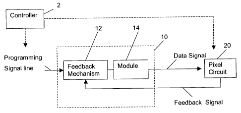
[0021 ] Figure 1 illustrates a pixel system for a feedback driving scheme in
accordance
with an embodiment of the present invention. The pixel system includes a pixel
circuit
20, a driver 10 for driving the pixel circuit 20, and a controller 2 for
controlling the
operation of the pixel system. The driver 10 includes a feedback module 12 and
a
module 14 for reducing the settling time and overshot for programming signals.
The
driver 10 may be shared by a plurality of pixel circuits in a column. The
pixel circuit 20
is selected by the controller 2. The driver 10 produces a data signal based on
a signal
on a programming signal line and a feedback signal from the pixel circuit 20.
The
feedback signal is associated with the OLED current. As described below, the
programming signal has an accelerating pulse. The accelerating pulse is set so
as to
accelerate the programming of the pixel circuit 20. The pixel circuit 20 may,
but not
limited to, have a current feedback, a voltage feedback, or an optical
feedback.
[0022] Figure 2 illustrates an example of the pixel system. The pixel circuit
20 of
Figure 2 includes a pixel driver having a driving TFT 22, switching TFTs 24
and 26, a
storage capacitor 28 and a feedback resistor 30 for driving an OLED 32. The
pixel
circuit 20 is fabricated with a-Si:H TFTs. The feedback resistor 30 is
fabricated with a
stable n+ amorphous or microcrystalline silicon layer, which is compatible
with the
TFT process and is used for fabrication of TFT contacts. However, in poly
silicon or
organic technology, the resistor can be fabricated using poly silicon and
organic
semiconductor/metallic material.
[0023] The anode terminal of the OLED 32 is connected to a voltage supply Vdd
and
the cathode terminal of the OLED 32 is connected to the first terminal of the
driving
TFT 22. The first terminal of the switching TFT 24 is connected to a data line
40. The
second terminal of the switching TFT 24, the gate terminal of the driving TFT
22, and
-4-
CA 02550102 2006-07-06
the first terminal of the storage capacitor 28 are connected at node Al. The
first
terminal of the switching TFT 26 is connected to a feedback line 42. The
second
terminal of the switching TFT 26, the second terminal of the driving TFT 22,
and the
second terminal of the storage capacitor 28 are connected to node B 1. The
gate
terminals of the switching TFTs 24 and 26 are connected to a select line 44.
The
resistor 30 is connected between node B1 and ground. The feedback line 42
transmits
to the column driver 10 a feedback signal associated with the OLED current.
[0024] In Figure 2, the feedback resistor 30 is in the pixel circuit 20.
However, the
feedback resistor 30 may be in the column driver 10, and thus be shared by a
plurality
of pixel circuits.
[0025] During the programming cycle, the pixel circuit 20 is connected to the
external
driving system through the data line 40 and the feedback line 42, forming a
voltage-controlled current source. After the programming cycle, the gate-
source
voltage VG of the driving TFT 22 is saved by the storage capacitor 28 thereby
allowing
the pixel circuit 20 to drive the OLED 32 with the appropriate programming
current.
[0026] In Figure 2, a differential amplifier is shown as an example of the
feedback
module 12 of Figure 1. In Figure 2, a lead compensator is shown as an example
of the
module 14 of Figure 1. The column driver 10 of Figure 2 includes the
differential
amplifier 12 with high voltage gain in series with the lead compensator 14.
The column
driver 10 maybe implemented in a high-voltage CMOS technology. The
differential
amplifier 12 may be an Op-Amp, such as a monolithic FET-input Op-Amp. The
differential amplifier 12 receives the feedback signal on the feedback line 42
and a
signal on a programming signal line Vin. The output of the differential
amplifier 12 is
provided to the lead compensator 14. The output of the lead compensator 14 is
connected to the data line 40. The lead compensation reduces the settling time
and
overshot for larger programming signal.
[0027] The transfer function of the compensator 14 is, for example, in the
form of
H(s)= (1 +siZ)/(1 +siP) . . . (1)
where tip<iZ for non-zero values of tiP and iZ. tiP and iz may be equal to
zero.
-5-
CA 02550102 2007-06-28
[0028] The values of -Ep and TZ are designed based on, for example, the
circuit
parameters such as parasitic capacitance of the data and feedback, gain and
unity-gain
bandwidth of the differential amplifier, the mobility of the thin film
transistors of the
pixel circuit, or combinations thereof. The lead compensation can enhance the
settling
time of the current in the AMOLED pixel circuit, preferably the settling time
at larger
programming currents associated with higher greyscales. The lead compensation
effectively reduces the settling time of the OLED current associated with
medium and
higher greyscale levels.
[0029] Circuit analysis and simulation results show that the smallest
programming
times are achieved if iZ satisfies:
1/(CFP Rs3) < TZ < 1/(Cs Rs2) ... (2)
where CFP is the parasitic capacitance of the feedback line 42 and Cs is the
storage
capacitor 28 of the pixel circuit 20. Rs2 and Rs3 are the ON resistance of the
switching
TFTs 24 and 26, respectively.
[0030] The operation of the pixel circuit 20 of Figure 2 is described in
detail. An
accelerating pulse is provided to the pixel circuit 20 to enhance the settling
as shown in
Figure 3. Figure 3 illustrates an example of waveforms for driving the pixel
circuit 20
of Figure 2. As shown in Figure 3, the signal on the programming signal line
Vin
includes (1) a primary accelerating pulse 50 between tl and t2 and (2) a pulse
52
between t2 and 0 with the desired programming voltage Vdata (tl<t2<t3). The
primary accelerating pulse 50 has a value Vpulse that is larger than the
desired
programming voltage Vdata. The accelerating pulse 50 increases the loop gain
and
boosts the charging of CFP at the beginning of programming and results in a
faster
programming.
[0031 ] During the programming mode tl-t3, the select line 44 goes high,
turning on the
switching transistors 24 and 26. Consequently, the driving transistor 22, the
feedback
resistor 30 and the differential amplifier 12 form a voltage-controlled
current source.
The feedback resistor 30 converts the current of the driving transistor 22 to
a voltage
VF. The voltage VF is then compared to Vin by the differential amplifier 12.
Due to the
inherent negative feedback in the circuit, the output of the column driver 10
adjusts the
-6-
CA 02550102 2006-07-06
gate voltage of the driving transistor 22. During tl-t2, the accelerating
pulse 50
increases the loop gain and boosts the charging of CFP, resulting in a faster
programming. During t2-t3, Vin goes to the desired programming level. The
pixel
circuit 20 compensates for the shift of the threshold voltage in the driving
transistor 22,
as long as the voltage VG at the gate of the driving transistor 22 does not
exceed the
maximum output range of the differential amplifier 12, and the voltage at the
select line
44 is high enough to turn on the switching transistor 24.
[0032] After t3, the select line 44 goes low, disconnecting the pixel circuit
20 from the
differential amplifier 12 by turning off the switching transistors 24 and 26.
The current
through the OLED 32 does not change considerably as the storage capacitor 28
stores
the gate-source voltage of the driving transistor 22.
[0033] The driving signals of Figure 3 are applied, for example, to the AMOLED
display for small programming currents. For large currents, Vpulse may be
equal or
even smaller than Vdata. The value of Vpulse is defined, for example, based on
the
parameters of the pixel circuit of Figure 2 and the value of Vdata.
[0034] Figure 4 illustrates a simulation result of the effect of the lead
compensation
(e.g., 14 of Figure 2) on the settling time of the OLED current. Since without
lead
compensation the system experience lots of ripples, the settling time
increases
dramatically. However, using the lead compensation controls the ripples and
thus
improves the settling time.
[0035] Figure 5 illustrates another example of the column driver 10 of Figure
1. The
column driver of Figure 5 includes a trans-conductance differential amplifier
60 with a
gain of Gm, a resistor 62, a voltage gain stage 64 with a gain of A, a
compensating MOS
transistor 66, and a capacitor 68. The differential amplifier 60 receives two
inputs V+
and V-. The voltage amplifier 64 receives the output of the differential
amplifier 60.
The transistor 66 and the capacitor 68 are connected in series between the
output of the
differential amplifier 60 and the output Vout of the voltage amplifier 64. The
resistor
62 converts the output current of the trans-conductance amplifier 60 to a
voltage for the
voltage amplifier 64.
-7-
CA 02550102 2006-07-06
[0036] The differential amplifier 60 corresponds to the differential amplifier
12 of
Figure 2. The combination of the gain stage 64, the transistor 66 and the
capacitor 68
corresponds to the lead compensator 14 of Figure 2.
[0037] The transistor 66 may be a NMOS or PMOS transistor or a transmission
gate.
The value of iZ is determined, for example, by the capacitance Cc of the
capacitor 68
and the resistance of the transistor 66. For fine tuning of the value of iZ,
the gate of the
transistor 66 is connected to a controlling voltage Vc.
[0038] Figure 6 illustrates simulation results of the feedback driving scheme.
In Figure
6, a waveform 70 is a programming current of an AMOLED pixel circuit with
feedback,
when driven by the feedback driving scheme having the accelerating pulse
(e.g., 50 of
Figure 3) and the lead compensator (e.g., 14 of Figures 1 and 2). In Figure 6,
a
waveform 72 is a programming current of an AMOLED pixel circuit with feedback,
when driven by a simple differential amplifier without the accelerating pulse
and the
lead compensator. As shown in Figure 6, the feedback driving scheme having the
accelerating pulse and the lead compensator is able to considerably improve
the
programming speed.
[0039] Figure 7 illustrates an example of a display system 80 that implements
the
feedback driving scheme. In Figure 5, SELi (i=1, 2, ...) represents a select
line, DLj
(j=1, 2, ...: column number) represents a data line, and FLj represents a
feedback line.
Each of SELI, SEL2, ... corresponds to the signal line 44 of Figure 1, each of
DLl,
DL2, ... corresponds to the data line 40 of Figure 1, and each of FL1 and FL2
,...
corresponds to the feedback line 42 of Figure 1. The data line DLj and the
feedback line
FLj (j=1, 2, ...) are shared by all the pixel circuits of the jth column. The
display system
80 includes a pixel array 82 in which a plurality of pixel circuits 20 are
arranged in row
and column. Preferably, the pixel array 82 is an AMOLED display. A data driver
84
and an address driver 86 are provided to the pixel array 82. The data driver
84 includes
a plurality of the column drivers 10, each of which is arranged in a column of
the pixel
array 82. The address driver 86 provides select signals SEL1, SEL2, ... The
address
driver 86 may drive Vc of Figure 5. The timing of each signal is controlled by
a
controller 88. The accelerating pulse 50 of Figure 3 is generated under the
control of
the controller 88.
-8-
CA 02550102 2007-06-28
[0040] In the description above, the pixel circuit 20 with voltage feedback is
shown as
an example of a pixel circuit to which the feedback driving scheme is applied.
However, the feedback driving scheme in accordance with the embodiments of the
present invention is applicable to any other pixel circuits with feedback.
[0041] The driving scheme of the embodiment of the present invention,
including the
pulsed shaped data and the lead compensated differential op-amp, accelerates
the
prograrnming of AMOLED feedback pixel circuits, such as voltage feedback pixel
circuits, cnirent feedback pixel circaits, and optical feedback pixel
circuits. The
combination of the lead compensator and the accelerating pulse improves the
programming speed at both high and low OLED currents.
[0042] By sending a feedback voltage from each pixel to the column driver
during the
programming cycle, the driving scheme can compensate for the instability of
the pixel
elements, e.g., the shift in the threshold voltage of TFfs.
[0043] The present invention has been described with regard to one or more
embodiments. However, it will be apparent to persons slcilled in the art that
a nuinber
of variations and modifications can be made without departing from the scope
of the
invention as defined in the claims.
-9-