Note: Descriptions are shown in the official language in which they were submitted.
I t.JI.J1 Irv% ort= \t-114, VO ..112 4272672
P.06
CA 02602365 2007-09-12
5710-2007 90 312 4272672
1B2006050406
DESCRIPTION
LOW-DIELECTRIC CONSTANT CRYPTOCRYSTAL LAYERS
AND NANOSTRUCTURES
= [1] The present invention relates to low-dielectric constant
cryptocrystals that may be used in
conjunction with future generation integrated circuits and devices. These
cryptocrystals
were grown by Chemical Vapor Processing (CVP) method [ S. Kalem and 0. Yavuz,
OPTICS EXPRESS 6, 7(2000)] consisting of the exposure of Silicon surface to
vapors of
acid mixtures. The cryptocrystal stands for a material that Is so finely
grained that no
distinct particles are discerned under optical microscope. State of matter
arranged in this
way with such minute crystals is said to be cryptocrystal or cryptogranuiar.
This type of
crystals can exhibit extraordinary properties which can be used in various
fields.
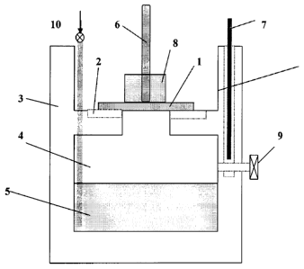
[2] The invention relates to cryptocrystals and particularly to Ammonium X
Fluoride (AXF),
which have been derived from state-of-the-art wafers and having a general
formula
(NH4)2XF6 - (wherein X =Si, Ge, C) named as 'ammonium X-fluoride'.
[3] There is no report In litterature on the above mentioned optical
quality dielectric
Ammonium X-Fluoride cryptocrystals.
[4] Ammonium Silicon Fluoride(ASiF) material was shown to be formed on
Silicon wafers
when Ammonium Fluoride NKIF is reacted with Si on the wafer surface [M_Niwano,
K.
Kurita, Y. Takeda and N.Miyamoto, Applied Physics Letters 62, 1003(1993)].
[5] As explained in another document, Ammonium Silicon Fluoride has been
found on the
walls of vacuum chambers and in the vacuum exhaust lines during plasma
assisted
semiconductor cleaning and deposition processings (S.Munley, I.McNaught,
D.Mrotek,
and C.Y.Lin, Semiconductor International, 10/1,( 2001)).
[6] It has also been shown that a light emitting powders of Ammonium
Silicon Fluoride can be
derived from porous Silicon using HF/HNO3 [M.Saadoun, B.Bessais, N.Mliki,
M.Ferid,
H.Ezzaouia, and R.Bennaceur, Applied Surface Science 210, 240(2003)].
[7] Similarly, [H.Ogawa, T.Arai, M.Yanagisawa, T.Ichlki and Y.Horiike, Jpn.
J. Applied physics
41, 5349(2002)] have shown that Ammonium Silicon Fluoride was formed on
Silicon
wafers when residual natural oxide reacts with hot Ammonium(NH3) and Nitrogen
Fluoride(NF3) on the wafer surface.
[8] Also, it was reported that ammonium silicon fluoride have been formed
when HF and NH3
=
gases are reacted on Si02 under vacuum. (P.D.Agnello, IBM J. of Research and
Development 46, Number 2/3, 2002)].
t91 There is no application quality cryptocrystal structure in the above
mentioned works.
Moreover, in these works ammonium silicon fluoride has been obtained as an
AMENDED SHEET
õfle
'""CA 02602365 2007-09-12 4(b(
F".tae
5:10-2007 90 312 4272672
I B2006050406
unintentional, irregular, disordered and contaminated by product.
[10] There Is no report in litterature on Ammonium X-Fluoride micro- and
nanowires.
(X=Silicon, Germanium, Diamond)
[11] There is no report on the fact that the dielectric constant of Ammonium X-
Fluoride
cryptocrystals can be tuned over a large scale and they can be used as
Insulator,
[12] Micro and nano-electronics are the most important fields of application
of this invention.
According to International Road Map for Semiconductors(ITRS) [C.Case, Solid
State
Technology, Jan., 47(2004)][P2eitzoff, R.W.Murto, H.R.Huff, Solid State
Technology,
71(2002)], semiconductor industry needs a low-dielectric constant(k)
intermetal insulators
with dielectric constant which is well under k=3Ø for high performance
Interconnections.
Therefore, it is very important to develop low-k dielectrics which are
compatible for future
integrated circuitry(IC) production. On the other hand, there is a continuing
effort in finding
a high-k dielectrics for CMOS gate insulation under 1 nanometer for 50
nanameter
fabrication node. Our invention also offers a solution to high-k issue with
cryptocrystal
layers whose dielectric constant can be set at a desired value by diffusion.
[13] In accordance with historical Moore law [G.E.Moore, Electronics 38,
114(1965)][
G.E.Moore, IEDM Technical Digest, Washington DC, 11(1975)] , down-scaling
continues
in CMOS technology. Multi-level metallisation is required to accomodate signal
integration
of a number of active elements. Electrical resistance and parasitic
capacitances in these
metal interconnects are important factors limiting the IC performance in next
generation
systems. This causes the industry to move from Aluminum-SiO2to Cupper/ low-k =
configuration. While the cupper decreases the line resistance, the low-k
dielectric
decreases the parasitic capacitance between metal lines.
[14] In order to overcome difficulties in downscaling of transistor
dimensions, the capacitance
per unit area is to be kept constant. Therefore, there is a need far high-k
value dielectrics.
These dielectrics can be oxides and silicates such as AI,03, Zr02, Hf02 . C.
J. Parker, G.
Lucovsky and J. R. Hauser, IEEE Electron. Device Lett. (1998); Y. Wu and G.
Lucovsky,
IEEE Electron. Device Lett. (1998); and H. Yang and G. Lucovsky, IEDM Digest,
(1999)
have suggested solutions in using these materials. However, there are very
tough
challenges to overcome concerning the economic cost and number of interfacial
defects.
Our cryptocrystal technology can offer potential solutions in this field. For
example,
maintaining advantages of natural gate oxide, a high-k dielectric can be
formed using
cryptocrystals. . ,
(15] The metal lines in integrated circuits are electrically insulated from
each other by dielectric
insulators. As the IC size becomes smaller, distances between metal lines are
decreased,
thus leading to an increased capacitances; This causes RC delays, power loss,
capacitively induced signals or cross-talks; There is a need for low-
dielectric
AMENDED SHEET
CA 02602365 2016-03-21
3
constant electrical insulation layers in lieu of Si02.
[16] Polymers with dielectric constant lower than that of S102 are used as
interconnect
insulator. But, the fact that the polymers are not strong, is an important
disadvantage.
[17] Oxides doped with Carbon can be a solution for the low-k dielectrics.
It is possible to obtain
oxides with dielectric constant smaller than 3Ø They present great
disadvantages
concerning durability.
[18] The performance characteristics gained by down sizing active circuit
elements in IC
production can be lost in interconnects and packaging elements. In this case,
not the
speed of transistor but the RC delays at interconnects become important.
Moreover, with
decreasing dimensions, deeper metal lines are required, thus making intermetal
capacitance more important than the interlevel capacitance. In order to
overcome these
difficulties superior low-k dielectrics and new fabrication methods are
required. Current
low-k dielectrics consist of oxides and polymers. Cryptocrystals can be a
potential solution
offering low-k potential. Thus, high performance IC's can be realized by
avoiding cross-
talks among adjacent electric circuits.
[19] One of the approaches is a method using air gaps to lower capacitances
[B.Shieh et. al.,
IEEE Electron Device Letters, 19, no.1, p.16-18(1998)] [DL. Wollesen, Low
capacitance
interconnection, US. Pat. No: 5,900,668, issued May 4, 1999]. In these
approachesi S102
has been used as interlevel and intermetal dielectric. U.S. Pat. Nos. US
5,470,802, US
5,494,858 , US 5,504,042 ve US 5,523,615 patents relate to the possibility of
decreasing
capacity by using air gaps. But, in these methods, harsh chemicals should be
used to form
air-gaps. Cryptocrystal technology can offer easier, damage free, low cost
solutions in
fabricating air-gaps or vias.
[20] This invention relates to ASiF cryptocrystals whose dielectric value
can be tuned by
several methods and can be synthesized on Si and Si-based wafers. By
diffusion, the
dielectric constant of ASiF cryptocrystals can be tuned from its minimum value
of 1.50 to
much higher values (desired). Thus, ferroelectric and optical emission
properties can be
possessed by cryptocrystals.
[21] This invention offers an important alternative to low-cost and high
performance low-k
technology. Because, it is derived from npotential integrated circuit wafers
and has a
dielectric constant lower than 2.00. This value is smaller than that predicted
by ITRS for
the year 2007 and beyond.
[22] This invention has important applications in Si CMOS technology and
GaAs technology, in
increasing the performance of heterojunction bipolar transistors (HBT), high
density
CA 02602365 2016-03-21
3a
information storage and information security, microelectronics packaging,
photonic
component production, IC system cooling, technology integration and sensor
production.
In accordance with one aspect, the invention provides a cryptocrystal method
of bonding
two wafers, wherein said wafers are electrically insulated by an air gap to
increase the
resilience of the devices to cross-talk and interference effects, the method
consisting of the
following steps:
a) treating a back surface of a first one of said two wafers for enhanced
bonding with a
second one of said two wafers, comprising the treatment of the back surface of
the first
wafer with vapor of HF:HNO3 chemical solution to transform selectively defined
back
surface of the first wafer to a low dielectric constant cryptocrystal layer of
(NH4)2SiF6 at a
growth rate of 1 pm/hour at room temperature;
b) removing the cryptocrystal layer of ammonium silicon hexafiuoride
(NH4)2SiF6 from the
back of the first wafer by rinsing the wafer in de-ionized water; thereby
forming an air gap
between the back surfaces of the two wafers, wherein walls of the air gap
comprise an
oxide of silicon ensuring further electrical insulation;
c) bonding the two wafers under vacuum together ensuring high frequency
electrical
insulation through the air gap formed between the back surfaces substantially
reducing
interference and cross-talk effects.
[23] The following figures relate to cryptocrystal properties, methods of
cryptocrystal
CA 02602365 2014-09-24
4
layer production and devices in which cryptocrystal layers can be used.
[24] Figure -1 Cryptocrystal production apparatus which is made of teflon,
consisting of a liquid
containing chamber exposure orifice, the sample holder, vapour exhaust
channels and
heater
[25] Figure -2 A detailed sketch of the sample holder where the wafer is
located.
[26]
[27] Figure -3 Cross-sectional micrograph of a cryptocrystal layer as taken
with Scanning
Electron Microscope(SEM) at 3.000 magnification. The thickness of this
cryptocrystal layer
is 21 pm.
[28] Figure -4 The interface between the cryptocrystal and the wafer as seen
at SEM with a
magnification of 7.500. The surface quality and the derivation of
cryptocrystals from wafer
are clearly shown. There is relatively smooth interface that is free from
cracks and cavities
and the cryptocrystal layer sticks well to the wafer.
[29] Figure -5 X-ray diffraction analysis show that the layers are
(NH4)2S1F6 and the crystals
belong to (4/m-32/m) isometric hexoctahedral system with Fm3m space group
[W.L.Roberts, G.R.Rapp and T.J. Cambell, Enc. of Minerals, 2nd Ed., Kluwer
Academic
Publishers, Dordrecht, 1990].
[30]
[31] Figure -6 It is possible to write selectively on the wafer surface to
form lithographic
structures without using photolithography. The figure shows the result of such
an experiment
[33] Figure -7 FTIR spectrum. The results of x-ray diffraction analysis
have been confirmed by
FTIR analysis through the presence of vibrational modes of (NH4)2SiF6
groupings. The
analysis indicate that the observed vibrational modes N-H and Si-F in at 480cm-
1, 725cm-1,
1433cm-1 and 3327cm -1 belong to N-H and Si-F bondings.
[34] Figure ¨8 SEM micrograph of a microwire that was formed under thermal
annealing.
CA 02602365 2014-09-24
,
. 5
[35]
[36]
[37]
[38] The numbers in figures and their correspondence are given below:
[39] 1.Wafer or Substrate
[40] 2.Gas exhaus channel,
[41] 3. Teflon container
[42] 4.Vapor chamber
[43] 5.Chemical mixture
[44] 6.Thermometer
[45] 7 Ph meter
[46] 8 Teflon block
[47] 9 Liquid exctraction valve
[48] 10 Nitrogen flashing valve
[49] 11 Process chamber orifice
[50] 12 ASiF cryptocrystals
[51] 13 Wafer and cryptocrystal interface
[52] 14(111) major diffraction peak
[53]
[54]
[55]
[56] 18 N-H vibrational modes
[57] 19 Si-0 vibrational mode
[58] 20 Si-F vibrational mode
[59] 21 Deformation mode
[60]
CA 02602365 2014-09-24
6
[77] A method for synthesizing ammonium silicon fluoride(ASiF) on Silicon
(Si) and Si based
wafers has been developed. In this method, we have used the vapor phase growth
technique that we have already developed [S. Kalem and 0. Yavuz, OPTICS
EXPRESS 6,
7(2000)]. With this method, we have grown cryptocrystal layers by having the
vapors of
Hidrofluoric Acid (HF) and Nitric Acid (HNO3) reacted on wafer surface.
Cryptocrystal layers
having white granular color were synthesized on wafers at 1pm/hour growth
rates.
[78] The advantages of this technique are: i) no electrical contacts are
required, ii)possibility of
writing on surfaces selectively, iii) layers are homogeneous, iv) thickness
can be controlled,
v) possibility of forming diffusion barrier in etching processes, vi) cost
effective compared to
other conventional techniques vii) has a cryptochrystalline property.
[79] Cryptocrystal ammonium silicon fluoride layers (NH.4)2SiF6 (ASiF) are
formed on state-of-the-
art-wafers when vapor of a mixture of conventional chemicals are reacted on
the surface of
wafers. This method is called as Chemical Vapor Processing (CVP) and involves
the
following steps:
[80] a) The preparation of teflon growth chamber and ultrasound cleaning
processes;
[81] b) Preparation of a chemical mixture containing HF:HNO3 with ratios (4-
10):(1-8) and 25-
50% hidrofluoric acid (HF) and 55-75% nitric acid (HNO3);
[82] c) Flushing the mixure with Nitrogen and priming the mixture for 10
seconds with a
piece of wafer;
[83] d) Closing entirely the orifice with a wafer to be processed;
[84] e) Making sure that the reaction products are evacuated from the
chamber through exhaust
channels;
[85] f) Controlling Ph and temperature;
[86] g) Cryptocrystal layers are formed on the wafer by Silicon mediated
coupling reactions
between HF and HNO3 species on the wafer surface following the equation
[87] X + 6HF + 2HNO3¨> (NR4)2XF6 + 302
[88] Wherein X can be Si, Ge or C.
[89] h) Wafer is transformed into a cryptocrystal layer at a rate of 1pm;
CA 02602365 2014-09-24
,
, 7
[90] i) Cryptocrystal layers can be annealed and their strength and density
can be enhanced;
[91] j) Transformation of cryptocrystals into nanostructures and
particularly to micro- and nan-
wires at above 50 C under nitrogen atmosphere.
[92] Here are the properties of wafers used in cryptocrystal layer
production:
[93] 1.Resistivities between 5-10 Ohm-cm
[94] 2.p-type, Boron doped, (100) and (111) oriented Si
[95] 3.n-type, Phosphor doped, (100) and (111) oriented Si
[96] 4.Silicon native oxide(thermal oxide) on Silicon Si02/Si
[97] 5.Stochiometric Si3N4 on Silicon (Si/Si3N4)
[98] 6.Si1,Gex, x<0.3 (Sil_xGex on Si)
[99] Cryptocrystal production apparatus consists of a substrate(1), gas
exhaust channel for
reaction by-products (2), teflon container (3), vapor processing chamber(4),
chemical
mixture(5), Ph meter (7), chemical extraction gate (9), heater(8) and
temperature
controller(6), orifice and sample holder(11) and nitrogen flashing(10).
[100] Cryptocrystal layers are composed of undiscernable particles (12) as
evidenced by optical
polarization microscope. The layer soaks all the visible light when examined
under optical
microscope thus not revealing any structural feature. What is seen under
microscope is as
though one looks at surface of the still standing water. Otherwise, we know
its chemical
structure through FTIR vibrational studies (Fig. 7) and its detailed
microstructure by SEM
investigation and its crystal structure by x-ray analysis (Fig. 5) indicating
that it is a
polycrystalline layer. In addition, the interface (13) roughness between the
cryptocrystal
layer and the wafer has an RMS value of less than 1000 nm and is free from air
gaps
or cracks as evidenced from SEM interfacial studies (see Fig.4).
[101] X-ray diffraction analysis indicate that the cryptocrystals grown
preferentially in the (111)
direction (14). Diffraction peaks and their relative intensitis are summarized
in Tablel.
[102] Table-1 X-ray diffraction data summarizing diffraction peaks observed in
cryptocrystals of
ASiF. Wherein, teta, d and 1/11 are diffraction angle, distance between planes
and
normalised diffraction intensities, respectively.
Peak No: 2 Teta (Degree) d
1/11
1 18.3401 4.83355
100
2 21.2009 4.18734 19
3 30.1452 2.96221 15
_
4 35.4952 2.52703 7
_
37.1360 2.41906 39
_
6 43.1362 2.09545 43
7 57.0333 1.61348 22
-
CA 02602365 2014-09-24
8
8 62.6247 1.48219 9
9 65.8394 1.41739 7
[103]
[104] Cryptocrystals(12) having white color, are formed on wafers(1) in the
form of regular thin
layers. The annealing experiments indicatate that ASiF stays on the surface up
to about
150 C. It is decomposed above this temperature.
[105] Depending on annealing temperature, bulk crystals(15) of ASiF are formed
on the surface.
The dimensions of these crystals can be up to 15pmx3Opm.
[106] Cryptocrystal can be selectively realized in any shape as dots(16),
wires and complex
branches including ordered flowers on wafers,
[107] Nanowires(17) with dimensions ranging from few nanometers up to one
micrometer and
lengths up to 50pm were produced. Moreover, variety of nanometer structures
and
particularly were produced.
[108] Room temperature optical properties of ASiF cryptocrystals exhibit the
vibrational peaks
as summarized in Table-2. The frequencies are associated with vibrations of
various
bonding configurations of N-H(18), Si-0(19) ve Si-F(20) modes in ASiF. The Si-
0
vibrations are related to the presence of a native oxide layer at the
interface.
[109] Table 2, A summary of FTIR data for ASiF cryptocrystals, wherein,
VS:Very Strong,
S:Strong, M:Medium, W:Weak, VW:Very Weak.
[110] Table 2
Frequency w(cm-1) Description Intensity
480 N-H wagging or Si-F deformation VS
725 Si- F stretching 725 Si
1083 Si-0 stretching (Str)
1180 Si-0 Asymmetric stretching(Asym Str)
1433 N-H Bending or deformation mode VS
2125 Si-H Stretching VW
3327 N-H symmetric stretching(sym str) VS
3449 N-H Degenerate stretching
[111]
[112] FTIR analysis indicate that ASiF has strong absorption notches at
3pm(18), 7pm(18),
13.6pm(20) and 20.8pm(21), and thus they can be used in optical applications.
[113] Deleted
CA 02602365 2014-09-24
. 9
[114] Deleted
[115] With increasing demand for ultra high density and high speed
applications, there is an
increasing interest for new high performance information storage systems
[H.Coufal and
G.W. Burr, International Trends in Optics, 2002] [ US Pat. No. 6,846,434]. In
another
application of this invention, we offer alternative solutions to solve high
performance
information storage. Using cryptocrystals, it would be possible to obtain
ultra-high density
memory cells(20) on electronic wafers. In this application it has been
possible to write
selectively on Silicon based wafers by forming cryptocrystal cells(16). The
fact that
cryptocrystals can have phase change(16) at relatively low temperatures,
offers the
possibility of erasing and rewriting. Thus, the fast phase change feature at
low
temperatures enables fast writing applications. Moreover, with 8.5 nm unit
cell dimension
of ASiF cryptocrystals, information storage densities of the order of Tb/cm2
can be
possible. Novelties brought by cryptocrystal technology in this field are: i)
possibility of
writing on microelectronic wafers without photolithography, ii) offer of high
density
information storage at Tb/cm2range, iii) high speed erasing and rewriting.
[116] Deleted
[117] This Invention can be used to bind two wafers together. The method
includes the formation
of cryptocrystal layers on the surfaces of both wafers by CVP and pressing two
wafers together
under H20, Nitrogen or Hidrogen(H2) at high temperature.