Note: Descriptions are shown in the official language in which they were submitted.
CA 02610656 2007-11-06
NEUROLOGICAL PROBE AND METHOD OF USING SAME
Field of the Invention
This invention relates to probes containing electrodes, particularly for use
in
neurological stimulation/lesioning and recording.
Background of the Invention
During neurosurgical procedures, electrodes are commonly used to monitor
electrical activity and stimulate and/or lesion neural tissue. Typically,
electrodes
are brought into the vicinity of cell membranes so that an electrical
transition
resistance (impedance) is created between the cells and the electrodes.
Electrical
stimulation of a malfunctioning neuron can be used to activate or reversibly
block
neural activity, while lesioning can be used to permanently disable neuronal
activity.
The recent resurgence of procedures to stimulate and produce lesions in
deep brain structures for the treatment of Parkinson's disease, tremor, and
dystonia, has been due not only to a better understanding of functional
neuroanatomy of the cells involved in these diseases, but also to the
development
of techniques for accurately localizing these cells. Microelectrode recording
allows
direct recording and characterization of the activity of neural cells and can
be used
to record individual cells at a spatial interval from a micron to 100 microns
and in a
frequency range from 600 Hz to 3000 Hz.
While microelectrodes provide the best means of localizing diseased cells,
generally, microelectrodes must be inserted into the brain multiple times
(e.g., at
target sites separated by about 2 mm) to sufficiently characterize the
physiology of
a region which is to be stimulated or lesioned. Probes comprising groups of
microelectrodes bundled together at high density ("multichannel
microelectrodes")
increase the resolution of individual recording passes, and can
stimulate/lesion
and record a 20-200 pm radius around an insertion site. Typically, a
multichannel
microelectrode is inserted at a location, and when a site of pathology is
identified,
it is removed and replaced by a larger diameter macroelectrode (e.g., about
1.1
1
CA 02610656 2007-11-06
,
mm) which is used to validate target location and for subsequent stimulating
and/or lesioning. However, even multichannel microelectrodes must be inserted
and removed at least three to five times to obtain good target localization
and
macroelectrodes generally must be inserted separately.
Multichannel electrodes which combine the recording functions of
microelectrodes and the stimulating functions of macroelectrodes have been
reported (see, e.g., US 5,282,468, US 2005/0246004, US 2006/0003090, US
7,010,356 and US 2006/0095105). However, there remains a need for less
intrusive custom configurable neurological probes that can simultaneously
provide
stimulation/lesioning and recording over a large field.
Summary of the Invention
There is provided a neurological probe comprising a plurality of stacked
electrode elements, each electrode element comprising a strip of electrically
non-
conductive substrate having incorporated therewith a first electrode for
providing
an electrical current and a second electrode for recording electrical
activity.
There is further provided a use of a probe of the present invention for
neurological modulation and/or measurements.
There is further provided a method of modulating and/or measuring
neurological activity of a nerve cell or tissue comprising: bringing a probe
of the
present invention into proximity of the nerve cell or tissue; and, determining
electrical current generated in the second electrode to measure neurological
activity of the nerve cell or tissue, and/or providing electrical current to
the first
electrode to stimulate or lesion the nerve cell or tissue.
There is further provided a method of treating a neurological disorder
comprising: bringing a probe of the present invention into proximity of a
nerve cell
or tissue implicated in the neurological disorder; and, providing electrical
current to
the first electrode to stimulate or lesion the nerve cell or tissue.
Individual electrode elements comprise a strip of electrically non-conductive
substrate, one or more first electrodes for providing an electrical current
and one
2
CA 02610656 2007-11-06
or more second electrodes for recording electrical activity. The first
electrode may
be used for stimulation and/or lesioning and the second electrode may be used
for
recording. Thus, stimulation/lesioning and recording can be performed without
the
need to remove or replace the probe. Preferably, each individual electrode
element comprises one first electrode and one second electrode. The substrate
provides support for the electrodes, facilitating stacking of electrode
elements to
provide a probe having multiple stimulating/lesioning channels and multiple
recording channels.
The substrate is a strip of material having length, width and thickness, with
the length being significantly greater in dimension than the width and
thickness.
The strips have flat surfaces to facilitate stacking. Stacking of strips, and
therefore electrode elements, preferably occurs in a direction perpendicular
to a
plane defined by the length and width and parallel to a plane defined by the
width
and thickness. Preferably, the width is also significantly greater in
dimension than
the thickness so that the strip itself is generally flat. Flatter strips
stacked in the
direction perpendicular to the plane defined by the length and width enhance
stability of the stack and permit stacking of more electrode elements in a
given
volume thereby providing more electrode channels in a probe of given size. The
ultimate dimensions (length and width) of the substrate depend on the
dimensions
of the electrodes, the number of electrodes supported by the substrate and the
use to which the probe is put. Preferably, the substrate is just large enough
to
accommodate the electrodes while providing sufficient support for its use in
the
desired application. Substrate thicknesses are preferably in a range of from
about
1 pm to about 100 pm, particularly about 5 pm to about 50 pm, for example
about
25 pm.
The substrate may comprise any electrically non-conductive material.
Preferably, the substrate material comprises a biocompatible material.
Preferably,
the substrate material is safe for use in medical applications, for example
neurosurgical applications. Plastics, for example polyimides (e.g. KaptonTm),
polyamides (e.g. Nylonn"), high density polyethylene (HDPE), fluoroethylene-
propylene polymer (FEP), polyparaxylenes (e.g. parylenes), silicones, are
useful
as substrate materials.
3
CA 02610656 2007-11-06
The electrodes may be located on or in the substrate, provided that at least
part of each electrode is exposed to the surrounding environment, preferably
at an
end (i.e. a tip) of the electrode. The electrodes are electrically insulated
from one
another on the substrate (i.e. no short circuits) and at least one part of
each
electrode can be electrically connected to another structure, preferably at an
end
of the electrode (connector end) opposite the tip.
Electrodes are preferably thin strips or wires. Strips have length, width and
thickness and wires have length and diameter. The length of the electrodes is
significantly longer than the width, thickness and/or diameter. Preferably,
the
length of an electrode is in a range of about 2 mm to about 300 mm, for
example
about 90 mm. Preferably, the width of an electrode is in a range of about 500
pm
or less, more preferably about 50 pm to about 500 pm, for example about 350
pm.
Preferably, the thickness or diameter of an electrode is about 100 pm or less,
more preferably in a range of about 10 A to about 100 pm, particularly about 5
pm
to about 25 pm, for example about 12.5 pm.
Electrodes comprise an electrically conductive material, preferably a
material resistant to degradation under conditions of use. Preferably, the
electrode material is platinum, titanium, gold, platinum-iridium or tungsten.
Platinum is of particular note.
The first and second electrodes have different impedances. The
impedance of the second electrode is greater than that of the first electrode.
Preferably, the impedance of the second electrode is about 100 times or more
greater than that of the first electrode, more preferably about 750 times or
more
greater. The impedance of second electrode is preferably about 100,000 ohms or
greater as measured at a frequency of 1000 Hz in a 0.9% NaCI solution, more
preferably in a range of about 150,000 ohms to about 500,000 ohms, for example
about 300,000 ohms. The impedance of the first electrode is preferably about
500
ohms or less as measured at a frequency of 1000 Hz in a 0.9% NaCI solution,
more preferably in a range of about 100 ohms to about 500 ohms, for example
about 350 ohms. Electrode impedances may be controlled by controlling the
amount of electrode material in the electrode, especially the area of
electrode
material exposed to the surrounding environment. The first electrode, i.e. the
4
CA 02610656 2007-11-06
stimulating/lesioning electrode, has more electrode material than the second
electrode, i.e. the recording electrode, therefore the first electrode has
less
impedance.
Preferably, frequencies at which recording electrodes are operated are in a
range of about 600 Hz to 3000 Hz.
Preferably, frequencies at which
stimulating/lesioning electrodes are operated are in a range of about 1 Hz to
about
500 Hz.
A wide variety of configurations of the electrodes on or in the substrate are
possible. Preferably, the first and second electrodes are substantially
coplanar on
or in the substrate, in a plane substantially perpendicular to the direction
of
stacking of the electrode elements. The exposed part of a second electrode in
an
individual electrode element is preferably separated from the exposed part of
a
first electrode in the same electrode element by a distance of about 0.1 mm or
more. More preferably, this distance is in a range of from about 0.1 mm to
about
2 mm, for example about 1 mm. Advantageously, changing the distance between
the first and second electrodes in an individual electrode element permits
custom
design of probe configurations, i.e. custom configuring of electrodes in a
probe.
Two or more electrode elements may be stacked to form the probe. The
probe preferably comprises four or more stacked electrode elements.
Preferably,
the number of stacked electrode elements is such that total cross-sectional
area
of the probe does not exceed 1000 pm x 1000 pm, more preferably does not
exceed 500 pm x 500 pm. A common ground may be used to ground all of the
electrodes in a probe.
Advantageously, electrode elements may be staggered in the stack in order
to stagger the positions of the first and second electrodes along the length
of the
probe. Staggering pattern, i.e. how adjacent electrode elements are disposed
in
relation to each other, is controllable permitting custom control of field
configuration. For example, staggering may result in a symmetric or asymmetric
stack of electrode elements. Each electrode in an electrode element provides a
channel. For example, an electrode element having one first electrode and one
second electrode has one stimulating/lesioning channel and one recording
5
CA 02610656 2007-11-06
channel for a total of two channels. Stacking eight of such electrode elements
provides a probe with sixteen channels, eight of which are
stimulating/lesioning
channels and eight of which are recording channels. By staggering the stacked
electrode elements in such a probe, the probe will have these sixteen channels
spaced out along its length so stimulation/lesioning and recording can be
effected
at eight different locations each without having to move the probe.
Staggering electrode elements results in off-setting channels in a stack by
an off-set distance along the length of the probe. Off-set distances in a
stack may
be the same or different. Preferably, the off-set distance between like
channels is
the same, i.e. the off-set distance between recording channels is the same and
the off-set distance between stimulating/lesioning channels is the same.
Preferably, the value of the off-set distance between recording channels is
the
same as the value of the off-set distance between stimulating/lesioning
channels.
The off-set distance is preferably in a range of from about 0.1 mm to about 1
mm,
for example about 0.5 mm. Advantageously, adjusting off-set distance permits
custom configuring of channels.
It is a great advantage of the probe of the present invention that fields are
highly custom configurable. The present invention offers at least four routes
to
controlling field configuration: controlling placement of the electrodes on
the
electrode element; controlling the staggering pattern of adjacent electrode
elements; controlling off-set distance between channels; and, stacking
electrode
elements permits tighter configuring of channels in the probe. Such
versatility is
highly advantageous. Furthermore, two or more stacks of electrode elements
may be clustered to further customize field configuration.
Each electrode may be electrically connected to another structure, for
example a measuring device and/or power source. To facilitate such electrical
connection, the probe may further comprise electrical connectors to which the
electrodes are attached. The electrical connectors of the probe may then be
connected to the other structure in ways well known in the art. Electrical
connectors may be, for example, pin connectors, plugs or snap connectors.
Attachment of the electrodes to the electrical connectors may be accomplished
by
known methods, for example soldering, snapping, crimping or gluing wires
6
CA 02610656 2007-11-06
between the electrodes and the electrical connectors, or plugging the
electrodes
directly into the electrical connector together with soldering, crimping or
gluing if
desired or required. The electrical connectors and the attachment of the
electrodes to the electrical connectors may be housed completely or partially
in a
protective housing.
Probes may further comprise a protective covering for the stack of
electrode elements. For example, the stack may be sheathed or partially
sheathed in a protective sheath that surrounds the stack covering regions of
the
stack that do not possess channels. The protective sheath may comprise any
suitably protective material, for example, stainless steel, plastic (e.g.
polyimide,
silicone, parylene), or combinations thereof.
In a process to fabricate a probe of the present invention, electrode
material is incorporated with electrically non-conductive substrate material
to form
electrode elements, and a plurality of electrode elements is stacked to form
the
probe. In forming an electrode element, the electrodes may be formed
separately
from electrode material and then incorporated with the substrate material, or
the
electrodes can be formed directly on or in the substrate material. Creating
strips
of electrically non-conductive substrate may be accomplished before or after
incorporation of the electrode material with the electrically non-conductive
substrate material.
Forming electrodes directly on or in the substrate may be accomplished by
incorporating electrode material directly into or onto the substrate material
by
physical methods such as evaporation, sputtering and laser ablation,
electrochemical methods such as electrodeposition and anodization, and
chemical
methods such as vapor deposition, sot-gel, spray photolysis, decomposition
reactions and thermal oxidation.
Preferably, electrodes are formed separately from electrode material and
then incorporated with the substrate material. Electrodes may be fabricated by
providing solid samples of the electrode material and forming the electrodes
from
the solid sample into the desired size and shape. Forming may be accomplished
by any suitable method, for example cutting, die stamping, electric discharge
7
CA 02610656 2007-11-06
=
machining (EDM), etching. Cutting may be accomplished by any suitable method,
for example, laser cutting, micro-milling, mechanical tools. The solid sample
of
electrode material may be provided in any form suitable for the desired
electrode
forming technique. For example, the solid sample may be a foil, plate or block
of
just electrode material, or a solid support having electrode material coated
thereon.
Once electrodes have been formed, they may be incorporated with the
substrate material. For example, electrodes may be affixed to a surface of the
substrate material, or may be encapsulated inside the substrate material.
Affixing
electrodes to the surface may be accomplished, for example, with an adhesive
(e.g. a holt-melt adhesive). Encapsulating the electrodes within the substrate
material may be accomplished, for example, by lamination of the electrodes
between layers of substrate material. Lamination may be accomplished with the
assistance of heat and/or adhesive. Coating the electrodes with substrate
material may be accomplished, for example, by vapor deposition.
Once the electrode elements have been formed, individual electrode
elements are stacked to form the probe. Stacking requires placing one
electrode
element next to another in proper alignment so that the electrode channels are
in
the proper position to provide the desired field. Electrode elements may be
stacked "back-to-back", "front-to-front", "back-to-front" or a combination
thereof in
a stack. Once properly aligned, electrode elements may be immobilized in
relation to the other electrode elements in the stack. Immobilization may be
accomplished, for example, with an adhesive.
Once electrode elements have been stacked, the probe may be finished by
attaching connectors to the electrodes, housing the connectors and attachment
points in a protective housing and providing a protective covering over the
stacked
electrode elements ensuring that the tip remains uncovered.
Probes of the present invention are particularly useful in biological
applications, especially medical applications. For example, they may be used
for
the stimulation and recording of activity in cells and tissues, and/or the
lesioning of
cells and tissues, especially nerve cells and tissues. The first electrode may
be
8
CA 02610656 2007-11-06
used for stimulating or lesioning, lesioning requiring providing more
electrical
current to the electrode. Neurological modulation and/or measurements may be
accomplished with probes of the present invention, which is particularly
useful in
assisting with neurosurgical procedures. Neurosurgical procedures may be used
to treat neurological disorders, for example, Parkinson's disease, Tourette's
syndrome, dystonia, tremors, slowness of movement, depression, rigidity,
epilepsy and eating disorders. The probe is especially useful for measuring
and
stimulating/lesioning brain and cortical neurons, particularly for deep brain
stimulation (DBS) or lesioning. The probe may be used for diagnostic purposes.
Probes of the present invention are less intrusive being of very small
diameter thereby reducing implantation trauma, yet can have a large number of
channels for stimulating/lesioning and recording. Electrodes have predictable
impedance, which improves functional reliability and consistency of
stimulation/lesioning and recording. Further, the ability to fabricate probes
with
custom configured stimulating/lesioning and recording fields permits the
production of highly specific and effective probes for any given specific
application. In neurosurgical applications, for example, such specificity is
highly
desirable as it enhances the ability of a surgeon to perform the correct
surgical
operations.
Further features of the invention will be described or will become apparent
in the course of the following detailed description.
Brief Description of the Drawings
In order that the invention may be more clearly understood, embodiments
thereof will now be described in detail by way of example, with reference to
the
accompanying drawings, in which:
Fig. 1 is a flow chart depicting a manufacturing process for fabricating a
neurological probe of the present invention;
Fig. 2 is a plan view of a platinum foil showing a pattern of electrodes cut
out of the foil;
9
CA 02610656 2007-11-06
Fig. 3A is a schematic top plan view of a first example of a fixture for
assembling electrode elements into a stack;
Fig. 3B is a schematic front elevational view of the fixture of Fig. 3A;
Fig. 3C is a schematic left side elevational view of the fixture of Fig. 3A;
Fig. 4A is a schematic top plan view of a second example of a fixture for
assembling electrode elements into a stack;
Fig. 4B is a schematic front elevational view of the fixture of Fig. 4A;
Fig. 4C is a schematic left side elevational view of the fixture of Fig. 4A;
Fig. 5 is a schematic of an assembled probe with protective sheath and
with connector and ground-wire connected;
Fig. 6A is a schematic plan view of a tip of an individual electrode element
for use in a first embodiment of a probe of the present invention;
Fig. 6B is a schematic plan view of a back end of the electrode element of
Fig. 6A;
Fig. 60 is a schematic perspective view of a tip of the first embodiment of a
probe of the present invention having eight stacked electrode elements;
Fig. 6D is a schematic cross-sectional side view of the tip of the probe
depicted in Fig. 6C;
Fig. 7A is a schematic plan view of a tip of an individual electrode element
of a second embodiment of a probe of the present invention;
Fig. 7B is a schematic plan view of a back end of the electrode element of
Fig. 7A;
Fig. 70 is a schematic perspective view of a tip of the second embodiment
of a probe of the present invention having eight stacked electrode elements;
CA 02610656 2007-11-06
Fig. 7D is a schematic cross-sectional side view of the tip of the probe
depicted in Fig. 7C;
Fig. 8A is a schematic plan view of a tip of an individual electrode element
of a third embodiment of a probe of the present invention;
Fig. 8B is a schematic plan view of a back end of the electrode element of
Fig. 8A;
Fig. 8C is a schematic perspective view of a tip of the third embodiment of
a probe of the present invention having eight stacked electrode elements; and,
Fig. 8D is a schematic cross-sectional side view of the tip of the probe
depicted in Fig. 8C.
Description of Preferred Embodiments
Referring to Fig. 1, a general process flowchart is depicted showing a
number of manufacturing steps for the fabrication of a probe of the present
invention. The preferred embodiments of the probe described herein comprise a
composite, stacked, staggered electrode element assembly with eight recording
channels and eight stimulating/lesioning channels, and composed of eight
individual electrode elements (each with one first electrode for
stimulating/lesioning and one second electrode for recording).
Three
embodiments of the probe are described below. The overall fabrication process
as described in Fig. 1 is similar in the three embodiments, with some
differences
at particular stages of the process.
Referring to Fig. 1, conceptual design drawings are prepared for the probe
of interest based on available neuronal signal detection information. The
concept
drawings are then translated into computer assisted design (CAD) drawings. The
CAD drawings are used as the basis for tool path planning for the electrodes
and
electrode element. Using CAD/CAM software, laser cutting and machining tool
path files are created from the original CAD drawings.
11
CA 02610656 2007-11-06
=
There are some differences in tool path planning for the three
embodiments. For the first embodiment, five different tool paths are used as
follows: a tool path for laser cutting of a conducting foil; a tool path for
laser depth
controlled machining of a tip area of an electrode; a tool path for adhesive
removal
in order to open a stimulation/lesioning area of a first electrode; a tool
path for
laser cutting of conductor supports to electrically separate first and second
electrodes; and a tool path for freeing up and removal of single electrode
elements. For the second embodiment, four different tool paths are used as
follows: a tool path for laser cutting of a conductor foil; a tool path for
laser depth
controlled machining of a tip (much smaller section) of an electrode; a tool
path for
laser cutting of conductor supports to electrically separate first and second
electrodes; and a tool path for freeing up and removal of single electrode
elements. For the third embodiment, four different tool paths are used as
follows:
a tool path for laser cutting of conductor foil; a tool path for laser depth
controlled
hole drilling of a recording channel of a second electrode; a tool path for
laser
cutting of conductor supports to electrically separate firs and second
electrodes;
and a tool path for freeing up and removal of single electrode elements.
Laser cutting and machining are accomplished with an integrated laser
machining workstation fitted with a nano- and femto-second pulse laser, an
optical
beam delivery system, a built-in camera optical viewing system and computer
controlled multi-axis motion system. A laser suitable for machining the
specific
material is integrated into a high precision CNC type multi-axis motion system
platform and controlled using tool path software. The CAD files of the
electrode
and electrode element pattern are used to develop the machine operating tool
path for the desired machining features. Feature precision and tolerances are
controlled during machining while applying optimal process parameters.
Additional
corrective patches of tool path commands are introduced into the software as
necessary to improve feature resolution at critical locations on the actual
pattern.
After several iterations and on-line/off-line measurements the machining tool
path
is optimized. Lasers are operated at wavelengths, selected from 1060 nm, 532
nm, 775 nm, 355 nm and 247 nm, depending on the specific material. Spectra
Physics YHP 40 laser, Ultra Violet AVIA 3W laser from Coherent, Clark-MXR
2010 fs model laser and Lambda Physik Excimer laser are examples of suitable
12
CA 02610656 2015-11-30
lasers. The laser, its control unit and the X,Y,Z axis motion system is
controlled
through encoders using a PC based control system which is integrated with user
interface software. The optical beam delivery system is mounted on the Z axis
along
with the focusing objective. The X, Y and Z axis resolution is 1 micron.
The laser machining workstation has a controlled air vacuum fixture securely
mounted
on to the XY stage. This vacuum fixture is leveled accurately across both X
and Y
directions of travel. Initially, the vacuum fixture can be setup using a high
resolution dial
indicator. Shim stock can be used to level the fixture appropriately. Shim
stock can be
used to shim the fixture level until a maximum of 5 pm height difference was
achieved.
To maximize utilization of conducting material, many individual first and
second
electrodes, and hence many individual electrode elements may be created from a
single sheet of electrically conducting foil. Electrodes are initially created
in the foil
sheet by laser cutting as follows. A piece of paper is placed on the vacuum
fixture and
a single 4"X4" sheet of 12.5 pm thick platinum conducting foil (available from
GoodfellowTM Corporation of Devon, PA, USA) is positioned on top right below
the
optical beam delivery system. Using a very slight, controlled vacuum suction,
the foil is
held in place laying flat minimizing wrinkles or dips. The optical viewing
system is used
to squarely align the foil sheet with respect to Y axis travel direction. Once
the sheet is
squarely placed, full vacuum force is applied and the foil is then ready for
laser cutting.
Laser cutting is controlled by the tool path created for the specific
electrode design
desired. For example, Fig. 2 shows the pattern of electrodes cut out of the
foil for the
third embodiment. Referring to Fig. 2, during laser cutting of the foil,
several
strategically located small supporting segments 201 (only one labeled) are
left uncut
between individual electrodes 202,203 (only one each labeled) in order to
maintain the
overall integrity of the foil sheet material. These support segments are
machined out
later after the electrodes are incorporated with the non-conductive substrate.
Once
laser cutting of the foil is complete, all the foil and paper debris is
cleaned off the
vacuum stage and the laser cutting process is repeated on a new sheet of foil.
Equipment and parameters for laser cutting of the foil are listed in Table 1.
13
CA 02610656 2015-11-30
Laser YHP-40
Wavelength 532 nm
Pulse repetition rate 20 kHz
Percentage of power 75%
Gas assist: air flow rate 11 L/min
Gas assist: air pressure 5 psi
Beam expander 10/10, 4x
Objective 5x
Motion system Aerotech X-Y-Z-U stages
Feed rate of foil 50 mm/min
Special requirements Vacuum table with plastic covering
around sample
After laser cutting, the foil sheet is cleaned by placing it in a container
filled with distilled
water and the container then placing it in an ultra,sonic cleaner for about 2
minutes to
remove any loose debris from the cut-out regions. Some debris may stick
together
with the foil and may not come out fully after the cleaning process. In that
case, manual
debris removal using a microscope and microtools is required. Once all debris
is
removed, the foil sheet is placed in a container filled with isopropanol,
which is then
placed in the ultrasonic cleaner for about 1 minute. The foil is allowed to
dry.
The laser cut foil sheet is then incorporated with a non-conductive substrate.
The non-
conductive substrate comprises KaptonTM, which is a polyimide. KaptonTM is
conveniently employed in the form of a polyimide film coated on one side with
a B-
staged modified acrylic hot melt adhesive available as PyraluxTM LF Coverlay
from
DuPontTM Electronic Materials of North Carolina, USA. For the first
embodiment, the
laser cut foil is bonded onto one surface of a 25 pm thick film of Kapton TM
with a 13 pm
thick layer of acrylic hot melt adhesive. For the second embodiment, the laser
cut foil
is encapsulated between two 13 pm thick films of KaptonTM, each film of
KaptonTM
having a 13 pm thick layer of acrylic hot melt adhesive for bonding. For the
third
embodiment, the laser cut foil is encapsulated between two 13 pm thick films
of
Kapton TM using a 13 pm thick layer of acrylic hot melt adhesive for bonding.
However,
for the third embodiment the top film of KaptonTM does not cover the tips of
the
electrodes thereby leaving the first electrode exposed. For all of the
embodiments,
connection points at the
14
CA 02610656 2007-11-06
back end of each electrode element are exposed on one side to facilitate
connection of wires to the connection points.
After incorporating the foil with the substrate, various steps are performed
to finish the electrode elements. For the first embodiment, a pre-defined
section
of the electrode material at the tip which was left without through cutting
during the
laser cutting process is machined using a depth controlled laser machining
method. A cyanoacrylate adhesive is applied to the foil on areas that were
machined. The adhesive is left to dry and the adhesive removal tool path is
then
used to expose the required stimulation/lesioning area. The second electrode
is
exposed by through cutting. For the second embodiment, laser depth controlled
machining is used to machine the KaptonTM off one side of the tip of the first
electrodes. The second electrodes are exposed by through cutting. For the
third
embodiment, a small hole is drilled out of the substrate using laser depth
controlled machining to expose an area of each second electrode. In all three
embodiments, small supporting segments that were previously left in are cut
out
by laser cutting. Individual electrode elements are freed up by laser cutting,
each
individual electrode elements comprising a strip of KaptonTM having one first
electrode and one second electrode incorporated therewith.
Laser depth controlled machining equipment for the three embodiments is
in Table 2. Laser depth controlled machining parameters for the first
embodiment
are in Table 3, and for the second and third embodiments in Table 4. Laser
cutting parameters for cutting electrode elements are in Table 5.
Table 2 ¨ Equipment for laser depth controlled machining
1st embodiment 2'
and 3rd embodiments
Laser YHP-40 AVIA
Wavelength 532 nm 355 nm
Beam expander 10/10, 4x 10/10, 4x
Objective 5x 5x
Gas assist Air Air
Motion system
Aerotech X-Y-Z-U stages Aerotech X-Y-Z-U stages
Special
Vacuum table with plastic Vacuum table with plastic
requirements covering around sample
covering around sample
CA 02610656 2007-11-06
Table 3 ¨ Parameters for laser depth controlled machining ¨ 1st embodiment
Laser pulse repetition rate - Pt machining 250 Hz
Laser percentage of power - Pt machining 58%
Laser pulse repetition rate - adhesive machining 1000 Hz
Laser percentage of power - adhesive machining 54%
Air flow rate 10 L/min
Feed rate ¨ Pt machining 40 mm/min
Feed rate ¨ adhesive machining 40 mm/min
Table 4 - Parameters for laser depth controlled machining ¨ 2nd and 3rd
embodiments
Laser pulse repetition rate 30 Hz
Laser percentage of power 36%
Thermal track of laser 6100
Air flow rate 10 L/min
Feed rate 75 mm/min
Table 5 ¨ Parameters for laser cutting of electrode elements
1st embodiment 2nd and 3rd embodiments
Laser YHP-40 AVIA
Pulse repetition rate 1 kHz 1 kHz
Percentage power 80% 80%
Thermal track of laser 4720 4720
Air flow rate 11 L/min 11 L/min
Feed rate ¨ support cutting _ 25 mm/min 25 mm/min
Feed rate ¨ freeing elements 75 mm/min 60 mm/min
Once the single electrode elements are freed up, they are placed in a
container filled with isopropanol and placed in the ultrasonic cleaner for
about 1
minute. Then the electrode elements are taken out of the isopropanol and
allowed
to dry. Once dried fully the electrode elements are placed in a clean
container
ready for the assembly process. Extreme care is necessary in handling these
flexible, delicate electrode elements.
Individual electrode elements are now checked for resistance between first
and second electrodes. Best case scenario would be an infinite resistance
between the electrodes. An arbitrary resistance of greater than 2 MCI was
chosen
as an acceptable value. The resistance test was conducted using a multimeter
16
CA 02610656 2007-11-06
with a 30 MO range. One lead was placed on the first electrode and the other
on
the second electrode on the back end of the individual electrode element. This
test was performed on each fabricated individual electrode element
Individual electrode elements are now stacked to form the probe. Any
suitable stacking method may be used. As individual electrode elements can be
very small in size, it is advantageous to employ a fixture for assembling a
stack of
electrode elements. Two embodiments of such fixtures and methods of stacking
electrode elements are described below.
A first example of a fixture for assembling a stack of electrode elements is
depicted in Figs. 3A-3C. In Figs. 3A-3C, all dimensions are in millimeters
(mm)
unless otherwise stated. Referring to Figs. 3A-3C, the fixture comprises upper
linear stage 301 and lower linear stage 302 from Newport Corporation
supporting
movable jaw 311, which is bolted on top of the upper linear stage. The linear
stages are bolted to base plate 304. Fixed jaw 312 is bolted on top of shim
block
305 disposed between the fixed jaw and the base plate. The shim block is
bolted
to the base plate. Upper linear stage 301 is fitted with fine pitch adjustment
screw
307 and lower linear stage 302 is fitted with digital micrometer 308. The
jaws,
shim block and base plate are made of aluminum.
The lower linear stage is used to offset the movable jaw from the fixed jaw
in a left-right direction. This facilitates staggered stacking of electrode
elements.
A desired off-set distance for stacked electrode elements may be achieved, for
example 0.5 mm. The digital micrometer, together with a microscope equipped
with a camera-based vision system, is used to set the desired off-set. The
upper
linear stage is used to open and close assembly gap 313 for holding the
electrode
elements in place. The fine pitch adjustment screw is used to adjust the size
of
the assembly gap.
To stack electrode elements into an assembled probe using the first
example of the fixture, the following process may be followed:
1. To start with, make the right hand edges of both jaws flush with
the digital
micrometer.
17
CA 02610656 2007-11-06
2. Set the micrometer to zero and move it back until it reads the desired
off-
set distance, e.g. 0.5 mm.
3. Place two electrode elements back to back in the assembly gap with the
exposed tips facing outward in the fixture on one marked edge.
4. Close the assembly gap using the fine pitch adjustment screw so the
electrode elements are snug together but movable.
5. Align the electrode element touching the fixed jaw with the edge of the
fixed
jam
6. Align the electrode element touching the movable jaw with the edge of
the
movable jaw.
7. Close the assembly gap further and apply adhesive to the edge of the
electrode elements in appropriate areas. Marked points on the fixture are used
to
identify the appropriate areas.
8. Open the assembly gap, take out the stacked electrode elements and flip
them 180 around the edge.
9. Place the stacked electrode elements back into the assembly gap and
align
the electrode element touching the fixed jaw with the edge of the fixed jaw.
10. Insert the next electrode element into the assembly gap with the
exposed
tip facing the movable jaw and aligned with the edge of the movable jaw which
is
shifted from the fixed jaw by the off-set distance.
11. Repeat steps 7 to 10 for all remaining electrode elements.
A second example of a fixture for assembling a stack of electrode elements
is depicted in Figs. 4A-4C. In Figs. 4A-4C, all dimensions are in millimeters
(mm)
unless otherwise stated. Referring to Figs. 4A-4C, the fixture comprises five
linear
ball slide assemblies 401 (only one labeled) (available from Del-Iron
Precision
Inc. of Bethel CT) on which five movable jaws 411a-e are bolted. The ball
slide
assemblies are bolted to base plate 404. Fixed jaw 412 is an integral part of
the
base plate. Five torsion wire springs 405 (only one labeled) connect each of
the
18
CA 02610656 2007-11-06
movable jaws to the base plate. The springs are bolted to the movable jaws
with
socket head cap screws 406 (only one labeled) and to the base plate with set
screws 408 (only one labeled). Five fine pitch adjustment screws 407a-e are
mounted in the base plate through threaded apertures so that the tip of each
fine
pitch screw contacts the movable jaws. The base plate, including the fixed
jaw,
and the movable jaws are made of aluminum.
The five ball slide assemblies permit movement of the five movable jaws in
response to actuation of the five fine pitch adjustment screws. Each of the
five
movable jaws can be controlled separately. Movement of the five movable jaws
results in opening and closing of assembly gap 413 in five regions along the
gap.
The assembly gap is used for holding the electrode elements in place during
the
stacking procedure. Having five movable jaws instead of one provides smaller
clamping areas along the length of the stack of electrode elements thereby
providing better control over alignment of the electrode elements.
Five
indentations 414 (only one labeled) identify position and application of
adhesive to
the stack without adhering to the jaws. Laser marked line 415 is inscribed in
fixed
jaw 412 and movable jaw 411a. This mark is used as a guide for off-set
distance.
More than one mark may be used if the off-set distance between adjacent
electrode elements is to differ as the stack is constructed.
The second example of the fixture provides improved alignment of
individual electrode elements, more precise stacking and better maintenance of
overall size within specifications in comparison to the first example of the
fixture.
To stack electrode elements into an assembled probe using the second
example of the fixture, the following process may be followed:
1. To start with, place two electrode elements back to back in the assembly
gap with the exposed tips facing outward in the fixture on one marked edge.
2. Tighten all the movable jaws using the fine pitch adjustment screws so
that
the electrode elements are snug together but movable.
3. Align the electrode element touching the fixed jaw with the edge of the
fixed
jaw.
19
CA 02610656 2007-11-06
4. Align the electrode element touching the movable jaws with the laser
marked line 415, which is the off-set distance (e.g. 0.5 mm) away from the
edge.
5. Tighten movable jaw 411a.
6. Push the edge of the electrode elements down so that they are touching
the bottom near movable jaw 411b then tighten movable jaw 411b.
7. Repeat step 6 for the remaining movable jaws of the fixture.
8. Loosen movable jaw 411a, push the electrode element down and tighten
movable jaw 411a.
9. Apply adhesive to the edge of the electrode elements in the indentations
on
the fixture and wait for the adhesive to dry.
10. Loosen the movable jaws, take out the stacked electrode elements and
flip
them 180 around the edge.
11. Place the stacked electrode elements back into the assembly gap and
align
the electrode element touching the fixed jaw with the edge of the fixed jaw.
12. Insert the next electrode element into the assembly gap with the
exposed
tip facing the movable jaws and align that electrode element with the laser
marked
line 415.
13. Repeat steps 5 to 12 for all remaining electrode elements.
When using either the first or second examples of the fixture to assemble
the third embodiment of the probe, one of the two electrode elements initially
placed in the assembly gap has the first electrode cut off.
Referring to Fig. 5, once the electrode elements have been stacked, wires
501 (only eight shown and only one labeled) are soldered on to each of the
electrodes, at the back end of the electrode elements, and the wires connected
to
28-pin multi-pin connector 502 (only 14 pins shown). For a probe of the first
embodiment, the two legs of the first electrode are jumped with a jumper wire
and
the jumper wire connected by another wire to the multi-pin connector. For a
probe
CA 02610656 2007-11-06
of the third embodiment, the back end of the electrode elements may be pushed
directly into the multi-pin connector and soldered for greater security. All
unused
connector pins are shorted and a common ground wire 503 is provided for the
entire stack. Epoxy may be applied over the individual wires and the connector
for insulation, rigidity and support, if desired. The probe is slid through
socket 504
and the socket glued to the sides of the connector to protect the connector
and
connecting wires. The socket comprises a non-conductive material, for example
a
plastic. Stainless steel tube 505 is placed over the probe to protect the
stack of
electrode elements without covering tip 506 where the stimulating/lesioning
and
recording channels are located.
Referring to Figs. 6-8, electrode and probe configurations are more
specifically described for the three embodiments. In Figs. 6-8, all dimensions
are
in millimeters (mm) unless otherwise stated.
Figs. 6A-6D depict electrode and probe configurations of the first
embodiment of the probe. Referring to Fig. 6A, tip of individual electrode
element
601 is depicted having electrode tip geometry such that first
(stimulation/lesioning)
electrode 602 is coplanar with and surrounds second (recording) electrode 603
in
U shape. The first electrode therefore has two "legs" 602a, 602b extending
back
to a back end of the electrode element, while the second electrode has one
"leg"
603a. As shown in Fig. 613, the legs of the electrodes terminate at the back
end in
widened portions 602c, 602d, 603c, which serve as connection points for
soldering connecting wires that connect the electrodes to a multi-pin
connector. A
jumper connection is used to connect the connecting wires from the two legs
602c, 602d of the first electrode before the wires are connected to the multi-
pin
connector.
Figs. 6C and 6D show eight individual electrode elements 601 (only one
labeled) stacked in a staggered fashion such that there is a
stimulating/lesioning
channel and a recording channel every 0.5 mm along the length of the probe
from
the tip to a position about 3.5 mm from the tip. Each electrode element
comprises
first electrode 602 (only one labeled) and second electrode 603 (only one
labeled)
on a strip of non-conductive substrate. The electrodes of the top four
electrode
21
CA 02610656 2007-11-06
elements face up while the electrodes of the bottom four electrode elements
face
down, thereby providing fields on opposite sides of the stack.
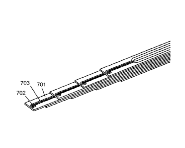
Figs. 7A-7D depict electrode and probe configurations of the second
embodiment of the probe. Referring to Fig. 7A, tip of individual electrode
element
701 is depicted having electrode tip geometry such that first
(stimulation/lesioning)
electrode 702 is coplanar with and "half-way curved" around second (recording)
electrode 703 in a partial U shape. Thus, the first electrode therefore has
only
one "leg" 702a extending back to a back end of the electrode element. The
second electrode also has one "leg" 703a. As shown in Fig. 7B, the legs of the
electrodes terminate at the back end in widened portions 702c,703c, which
serve
as connection points for soldering connecting wires that connect the
electrodes to
a multi-pin connector.
Figs. 7C and 7D show eight individual electrode elements 701 (only one
labeled) stacked in a staggered fashion such that there is a
stimulating/lesioning
channel and a recording channel every 0.5 mm along the length of the probe
from
the tip to a position about 3.5 mm from the tip. Each electrode element
comprises
first electrode 702 (only one labeled) and second electrode 703 (only one
labeled)
on a strip of non-conductive substrate. The electrodes of the top four
electrode
elements face up while the electrodes of the bottom four electrode elements
face
down, thereby providing fields on opposite sides of the stack.
The design of the second embodiment is superior to the first embodiment
since it eliminates the jumper connection at the connector and thus enables
the
use of a smaller connector as well as reduces complexity in the fabrication
and
assembly. The fabrication process is also improved in that impedance
variability is
reduced between the electrodes on separate electrode elements and controlled
depth machining is almost eliminated resulting in faster and more accurate
machining of the electrodes.
Figs. 8A-8D depict electrode and probe configurations of the third
embodiment of the probe. Referring to Fig. 8A, tip of individual electrode
element
801 is depicted having electrode tip geometry such that first
(stimulation/lesioning)
electrode 802 is coplanar with second (recording) electrode 803. First
electrode
22
CA 02610656 2007-11-06
802 is L-shaped having a larger area region at the tip 807, the size of which
is
selected to provide the proper impedance for the first electrode. The tip of
second
electrode 803 is bent inward toward the first electrode and is rounded at the
end.
The tip of the second electrode has a blind pocket (partial hole) 808 or a
small
controlled area opening to provide proper impedance for the electrode. The
first
electrode has one "leg" 802a extending back to a back end of the electrode
element. The second electrode also has one "leg" 803a. As shown in Fig. 8B,
the
legs of the electrodes terminate at the back end in widened portions
802c,803c,
which serve as connection points for connection of the electrodes to a multi-
pin
connector. The shape of the widened portions is such that the back end of the
electrodes can plug directly into the pins of the multi-pin connector, which
may be
followed by soldering to ensure secure attachment.
Figs. 8C and 8D show eight individual electrode elements 801 (only one
labeled) stacked in a staggered fashion such that there is a
stimulating/lesioning
channel and a recording channel every 0.5 mm along the length of the probe.
Each electrode element comprises first electrode 802 (only one labeled) and
second electrode 803 (only one labeled) on a strip of non-conductive
substrate.
The electrodes of the top four electrode elements face up while the electrodes
of
the bottom four electrode elements face down, thereby providing fields on
opposite sides of the stack.
The design of the third embodiment is superior to the first and second
embodiments. The third embodiment requires fewer machining steps to fabricate
than the other two embodiments, requiring no depth controlled machining at all
for
the first electrode. Impedance variability between electrodes is even more
reduced than the second embodiment and the impedances of the electrodes are
more suited for neurosurgical applications. The third embodiment is more
compact than the first embodiment, and the back end can be connected directly
to
the multi-pin connector obviating the need for connecting wires.
Other advantages that are inherent to the structure are obvious to one
skilled in the art. The embodiments are described herein illustratively and
are not
meant to limit the scope of the invention as claimed. Variations of the
foregoing
23
CA 02610656 2007-11-06
embodiments will be evident to a person of ordinary skill and are intended by
the
inventor to be encompassed by the following claims.
24