Note: Descriptions are shown in the official language in which they were submitted.
CA 02614803 2007-10-05
WO 2006/105638
PCT/CA2006/000492
MBM File No 1037-150PCT
ELECTRONIC DEVICE PACKAGE WITH AN
INTEGRATED EVAPORATOR
FIELD OF THE INVENTION
[0001] The present invention pertains to the field of electronic device
packaging and
in particular to a packaging design enabling thermal coupling to a thermal
management
system.
BACKGROUND
[0002] Electronics packaging involves providing electrical and
mechanical
connections, as well as providing protection, to, for example, a semiconductor
chip.
This field has been developing, and substantially started with metal or
plastic based
compound material packaging configurations.
[0003] Having specific regard to thermal management, packaging designs
have
improved over time for the removal of waste heat generated by the electronic
devices.
Typically, an electronic device for example, a semiconductor device, can fail
when its
junction temperature exceeds a certain threshold. The increasing power
consumption
trends of contemporary semiconductor devices can require sophisticated
packaging that
can handle large thermal loads. Some of the semiconductor chips commercially
available today, require packaging which can dissipate waste heat at about
100W per
device. Light-emitting diodes (LEDs) can be included in this category.
[0004] Presently, heat pipes, thermosyphons, liquid coolers and other
techniques, for
example, are used in power electronics or digital processors to spread the
heat load over
a large area for dissipation of this heat to the environment, or transfer of
the heat to an
alternate location where free or forced flow of gas or liquid can enhance heat
dissipation. Typically, traditional electronic device packaging is interfaced
to a heat
pipe or heat transfer system, by attaching the evaporator end of the heat
transfer system
to the outside of the packaging, as illustrated in Figure 1. Generally, this
technique
1
CA 02614803 2007-10-05
WO 2006/105638
PCT/CA2006/000492
MBM File No. 1037-150PCT
provides an adequate but not optimal thermal interface to move and spread the
heat
generated by the electronic devices. This technique does however, allow for
relatively
inexpensive manufacturing of the package, as standard packaging processes and
standard equipment can be used.
[0005] A downfall of current thermal solutions is that there is an undesirable
thermal
resistance that exists between the package and the thermal management system,
for
example a heat pipe. This fact can result in an increase in the junction
temperature of
the semiconductor material or electronic devices, thereby resulting in reduced
performance and a possible shorter lifetime thereof. With further reference to
Figure 1,
an elevated side view of an assembly of a light emitting diode package and a
heat pipe
30 as is known in the art is illustrated. The light emitting diode package
comprises a
number of light-emitting diodes 40 which are affixed to and in thermal contact
with a
substrate 20. The substrate is in thermal contact with a carrier or a housing
10 which is
in thermal contact with the heat pipe. This package design has to conduct heat
from the
light-emitting diodes 40 to the heat pipe 30, however, minute changes in
manufacturing
or assembly tolerances can compromise heat transfer across the interfaces
between the
light-emitting diodes, the substrate, the carrier or housing, and the heat
pipe. As such,
the overall heat transfer capability, mostly through heat conduction is
typically sub-
optimal.
[0006] United States Patent No. 5,355,942 discloses a method and apparatus for
cooling a multi-chip module using heat pipes. The semiconductor chips are
dispose into
the multi-chip module through cavities in the module substrate, wherein the
semiconductor chips engage the embedded heat pipes. This multi-chip module
design
includes a number of speciality requirements, including the creation of
cavities within
and along the length of the substrate, wherein it may not be possible to
manufacture this
requirement during standard electronic device package manufacturing.
[0007] United States Patent Application Publication No. 2005/0231983 discloses
an
apparatus comprising at least one heat pipe wherein each heat pipe has a first
end and a
second end and a cavity extending from the first end to the second end and a
light
emitting device mounted to and contacting the first end of each heat pipe. The
light
emitting device attach being mounted directly onto the heat pipe and such that
the
2
CA 02614803 2007-10-05
WO 2006/105638
PCT/CA2006/000492
MBM File No. 1037-150PCT
mounting configuration is free from any intervening substrate between the
light emitting
device and heat pipe. As the light emitting device is mounted directly onto
the heat
pipe, the pipe would progress with any package through the entire
manufacturing
process thereof. Therefore the size of the heat pipe would be directly
impacted by
standard package manufacturing machinery, thereby potentially limiting the
effectiveness of the heat extraction capability of the heat pipe.
[0008] Therefore there is a need for a new packaging design that can be
assembled
using standard package manufacturing techniques while additionally providing a
desired
level of thermal transmission from the package to a thermal management system
associated with the package.
[0009] This background information is provided for the purpose of making known
information believed by the applicant to be of possible relevance to the
present
invention. No admission is necessarily intended, nor should be construed, that
any of
the preceding information constitutes prior art against the present invention.
SUMMARY OF THE INVENTION
[0010] An object of the present invention is to provide an electronic device
package
with an integrated evaporator. In accordance with an aspect of the present
invention,
there is provided an electronic device package adapted for enabling thermal
regulation,
said electronic device package comprising: an evaporator portion adapted for
operable
coupling to a secondary portion of a thermal management system; one or more
electronic devices thermally connected to the evaporator portion; and a
housing coupled
to the evaporator portion.
BRIEF DESCRIPTION OF THE FIGURES
[0011] Figure 1 illustrates a cross section of a light emitting diode package
coupled to
a heat pipe according to the prior art.
[0012] Figure 2 illustrates a cross section of an electronic device package
according to
one embodiment of the present invention.
3
CA 02614803 2007-10-05
WO 2006/105638
PCT/CA2006/000492
[0013] Figure 3 illustrates an electronic device package according to one
embodiment
of the present invention, upon interconnection with the secondary portion of
the thermal
management system.
[0014] Figure 4 illustrates an electronic device package according to one
embodiment
of the present invention, coupled to a horizontally oriented thermal
management system.
[0015] Figure 5 illustrates an electronic device package according to another
embodiment of the present invention, coupled to a horizontally oriented
thermal
management system.
[0016] Figure 6 illustrates an electronic device package according to one
embodiment
of the present invention, aligned with and prior to coupling to thermal
management
system
[0017] Figure 7 illustrates the electronic device package of Figure 6, coupled
to the
thermal management system.
[0018] Figure 8 illustrates a cross section of an electronic device package
according to
another embodiment of the present invention, further illustrating continuity
of wicking
material for coupling of the evaporator portion of the electronic device
package to the
secondary portion of the thermal management system.
[0019] Figure 9 illustrates a cross section of an electronic device package
formed
around the end of a heat pipe according to another embodiment of the present
invention.
[0020] Figure 10 illustrates a cross section of an electronic device package
formed
around the end of a heat pipe according to another embodiment of the present
invention.
DETAILED DESCRIPTION OF THE INVENTION
Definitions
[0021] The term "electronic device" is used to define any device wherein its
level of
operation depends on the current being supplied or the voltage being applied
thereto.
An electronic device can be a light emitting element, electronics,
semiconductor chip,
4
CA 02614803 2007-10-05
WO 2006/105638
PCT/CA2006/000492
motor or any other device requiring electrical current or voltage regulation
as would be
readily understood by a worker skilled in the art.
[0022] The term "light-emitting element" is used to define any device that
emits
radiation in any region or combination of regions of the electromagnetic
spectrum for
example, the visible region, infrared and/or ultraviolet region, when
activated by
applying a potential difference across it or passing a current through it, for
example.
Therefore a light-emitting element can have monochromatic, quasi-
monochromatic,
polychromatic or broadband spectral emission characteristics. Examples of
light-
emitting elements include semiconductor, organic, or polymer/polymeric light-
emitting
diodes, optically pumped phosphor coated light-emitting diodes, optically
pumped nano-
crystal light-emitting diodes or any other similar light-emitting devices as
would be
readily understood by a worker skilled in the art.
[0023] The term "thermal management system" is used to define an element
providing
a means for thermal energy transfer. A thermal management system can be
designed to
incorporate thermal removal techniques including but not limited to conductive
and
convective cooling, liquid cooling, phase change cooling and forced air
cooling.
Thermal management systems can comprise heat pipes, thermosyphons,
thermoelectrics,
thermotunnels, spray cooling system, macro or micro channel cooling systems,
thermoelectric cooling systems or other appropriate thermal management systems
as
would be known to a worker skilled in the art.
[0024] As used herein, the term "about" refers to a +/-10% variation from the
nominal
value. It is to be understood that such a variation is always included in any
given value
provided herein, whether or not it is specifically referred to.
[0025] Unless defined otherwise, all technical and scientific terms used
herein have
the same meaning as commonly understood by one of ordinary skill in the art to
which
this invention belongs.
[0026] The present invention provides an electronic device package that can be
fabricated using standard package fabrication technologies while providing a
desired
level of thermal transfer capability to an attachable thermal management
system. The
electronic device package according to the present invention comprises a
housing that is
5
CA 02614803 2007-10-05
WO 2006/105638
PCT/CA2006/000492
specifically designed to couple with an evaporator portion of a thermal
management
system, for example a heat pipe. One or more electronic devices are mounted in
thermal
contact with the evaporator portion of the thermal management system. Upon
completion of the fabrication of the package using standard techniques, the
evaporator
portion of the electronic device package is operatively coupled with a
secondary portion
of the thermal management system. In this manner the electronic device package
can be
fabricated to incorporate a desired thermal management system, while being
fabricated
using standard package fabrication processes and machinery.
100271 The electronic device package of the present invention can reduce the
number
of interfaces between electronic devices and a thermally attached thermal
management
system across which a desired level of heat transfer can be maintained in
order to be able
to efficiently cool the electronic devices under operating conditions.
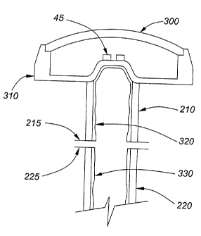
10028] Figure 2 illustrates an elevated cross section of an electronic device
package
according to one embodiment of the present invention. The electronic device
package
comprises an integrated assembly of one or more light-emitting elements 45
which are
affixed in thermal contact with an evaporator portion 210 of a heat pipe. The
heat pipe
comprises a secondary portion 220 which is partially shown and can be part of
a larger
thermal management system. The electronic device package additionally
comprises a
housing 310 which may optionally include an optical element or optical system
300. A
part of the housing proximal to the light-emitting elements 45 can be
sealingly affixed to
provide a cap to the evaporator portion 210 of the heat pipe. The evaporator
portion 210
can be sealingly attached to the heat pipe secondary portion 220 to form a
sealed heat
pipe. The evaporator portion 210 and the secondary portion 220 can be lined
with a
structure of wicking material 320 and 330, respectively, wherein the wicking
material
320 and 330 is configured to provide continuity between the evaporator portion
and the
secondary portion. This continuity of the wicking material can enable the
transfer of a
working fluid between the evaporator portion and the secondary portion. The
evaporator
portion and the secondary portion can have mating structures for mechanical
connection
thereof. Figure 2 illustrates these mating structures as cooperating flanges
215 and 225.
The heat pipe formed from the sealing connection of the evaporator portion and
the
secondary portion would be charged with a suitable working fluid for enabling
the
functionality of the heat pipe, wherein a suitable working fluid can be for
example water
6
CA 02614803 2007-10-05
WO 2006/105638
PCT/CA2006/000492
or other fluid or cooling substance as would be readily known to a worker
skilled in the
art.
Evaporator Portion
[0029] In embodiments of the present invention, the thermal management system
can
be a heat pipe, a thermosyphon, a heat exchanger, a Peltier cooler or any
other
component providing passive or active cooling as is known in this art. It is
understood
that the thermal management system or cooling system can comprise one or more
assembled suitably dimensioned components.
[0030] The electronic device package according to the present invention
comprises an
evaporator portion of the thermal management system to which the electronic
device
package is to be thermally connected. The evaporator portion of the thermal
management system is a location of heat entry into the thermal management
system,
wherein the thermal management system subsequently provides for the
dissipation of the
heat generated by the one or more electronic devices thermally coupled
thereto.
[0031] The evaporator portion is configured to mate with a secondary portion,
wherein
upon a required level of coupling between the evaporator portion and the
secondary
portion, the thermal management system can be capable of dissipating the heat
generated
by the one or more electronic device thermally connected thereto.
[0032] In one embodiment of the present invention, the evaporator portion
comprises
both wicking structure and an external support structure, wherein the wicking
structure
enables fluid transfer to the secondary portion of the thermal management
system, and
the external support structure can provide a means for the mating coupling
between the
evaporator portion and the secondary portion.
[0033] In another embodiment of the present invention, the evaporator portion
is
configured solely as a wicking structure, wherein the evaporator portion can
be inserted
into the secondary portion of the thermal management system. In this
embodiment,
sealing between the electronic device package and the secondary portion can be
provided by a sealing connection between the housing and the secondary portion
being
formed.
7
CA 02614803 2007-10-05
WO 2006/105638
PCT/CA2006/000492
[0034] In one embodiment of the present invention, the evaporator portion and
the
secondary portion each comprise flanges configured to matingly connect the
evaporator
portion and the secondary portion.
[0035] In another embodiment of the present invention the evaporator portion
and the
secondary portion are positioned to align with each other. A collar or cover
plates are
coupled to both the evaporator portion and the secondary portion in order
provide
operational connection between the evaporator portion and the secondary
portion.
[0036] In one embodiment of the present invention, the longitudinal axis of
the
thermal management system is substantially perpendicular to the plane on which
the one
or more electronic devices are mounted. Therefore the evaporator portion of
the
electronic device package defines one end of the thermal management system,
upon the
operative coupling of the evaporator portion and the secondary portion.
[0037] In another embodiment of the present invention, the longitudinal axis
of the
thermal management system is substantially parallel to the plane on which the
one or
more electronic devices are mounted. In this configuration, the evaporator
portion of the
electronic device package can define a position along the length of the
thermal
management system formed from the coupling of the evaporator portion and the
secondary portion. For example, the evaporator portion can mate with the
secondary
portion in a central region of the secondary portion.
[0038] In one embodiment of the present invention, the evaporator portion is
integrally formed with a substrate, wherein the substrate is configured with a
surface
roughness that can be capable of forming and functioning as a wicking
structure. The
secondary portion of the thermal management system, for example the secondary
part of
a heat pipe, comprises a wicking material which is capable of contacting the
substrate at
the roughened location and can be affixed thereto on the substrate. The
substrate can be
formed from a ceramic, metal or other material which can be configured to have
the
desired level of roughness. For example the substrate can be mechanically or
chemically
altered to enhance the roughness thereof, thereby enhancing the wicking
characteristics
of that location of the substrate. The substrate may alternately be etched in
a manner
8
CA 02614803 2007-10-05
WO 2006/105638
PCT/CA2006/000492
that produces a heat exchanger structure for non-phase change liquid cooling
applications.
[0039] In one embodiment of the present invention, the evaporator portion is
configured as the evaporator of a heat pipe, wherein upon coupling to a
secondary
portion the completed heat pipe provides for heat transfer away from the one
or more
electronic devices associated with the electronic device package.
[0040] In one embodiment, the evaporator portion can be coated with a
thermally
conductive or a non thermally resistive dielectric material, wherein the
dielectric
material can be patterned to provide electrical traces for the supply of
electrical current
to the one or more electronic devices.
Electronic Devices
[0041] An electronic device is any device wherein its level of operation
depends on
the current being supplied or the voltage being applied thereto. An electronic
device can
be a light-emitting element, electronics, semiconductor chip, motor or any
other device
requiring electrical current or voltage regulation as would be readily
understood by a
worker skilled in the art.
[0042] In one embodiment of the present invention, the one or more electronic
devices
are one or more light-emitting elements that are selected to provide a
predetermined
colour of light. The number, type and colour of the light-emitting elements
within the
electronic device package may provide a means for achieving high luminous
efficiency,
a high Colour Rendering Index (CRI), and a large colour gamut, for example.
The one
or more light-emitting elements can be manufactured using either organic
material, for
example OLEDs or PLEDs or inorganic material, for example semiconductor LEDs.
The one or more light-emitting elements can be primary light-emitting elements
that can
emit colours including blue, green, red or any other colour. The one or more
light-
emitting elements can optionally be secondary light-emitting elements, which
convert
the emission of a primary source into one or more monochromatic wavelengths or
quasi-
monochromatic wavelengths for example blue or UV pumped phosphor or quantum
dot
white LEDs or blue or UV pumped phosphor green LEDs or other LED formats known
in the art. Additionally, a combination of primary and/or secondary light-
emitting
9
CA 02614803 2007-10-05
WO 2006/105638
PCT/CA2006/000492
elements can be provided within the package, and can be determined based on
the
desired light output from the lighting device package.
[0043] In one embodiment, a electronic device package comprises light-emitting
elements having spectral outputs corresponding to the colours red, green and
blue can be
selected, for example. Optionally, light-emitting elements of other spectral
output can
additionally be incorporated into the electronic device package, for example
light-
emitting elements radiating at the red, green, blue and amber wavelength
regions or
optionally may include one or more light-emitting elements radiating at the
cyan
wavelength region. Optionally, light-emitting elements emitting colours
corresponding
to warm white, green and blue can be selected. The selection of light-emitting
elements
for the electronic device package can be directly related to the desired
colour gamut
and/or the desired maximum luminous flux and colour rendering index (CRI) to
be
created by the electronic device package.
[0044] In another embodiment of the present invention, the electronic device
package
comprises a plurality of light-emitting elements that are combined in an
additive manner
such that any combination of monochromatic, polychromatic and/or broadband
sources
is possible. Such a combination of light-emitting elements includes a
combination of
red, green and blue (RGB), red, green, blue and amber (RGBA) and combinations
of
said RGB and RGBA with white light-emitting elements. The combination of both
primary and secondary light-emitting elements in an additive manner can be
used in the
lighting device package. Furthermore, the combination of monochromatic sources
with
polychromatic and broadband sources such as RGB and white and RGBA and white
may also occur in the electronic device package. The number, type and colour
of the
light-emitting elements can be selected depending on the lighting application
and to
satisfy lighting requirements in terms of a desired luminous efficiency and/or
CRI.
Housing
[0045] The housing of the electronic device package is coupled to the
evaporator
portion and the housing can provide one or more functions comprising
electrical
connectivity to the one or more electronic devices, environmental protection
of the one
CA 02614803 2007-10-05
WO 2006/105638
PCT/CA2006/000492
or more electronic devices, support structure for the one or more electronic
devices and
the like.
[0046] In one embodiment, the housing can be configured to extract, modify or
direct
light from an opto-electronic device positioned in the electronic device
package.
[0047] In one embodiment of the present invention, the housing completely or
partially encloses the one or more electronic devices.
[0048] In one embodiment, the housing comprises a substrate which includes two
parts, namely a carrier portion and a thermally conductive portion. The
substrate is
configured for ease of thermal connection between the evaporator portion and
the
thermally conductive portion. For example, the carrier portion can be a
silicon layer
upon which is formed a layer of CVD diamond or other thermally conductive
material
for example a thermally conductive ceramic selected from AIN, Be0, Alumina or
other
ceramic as would be readily understood by a worker skilled in the art, which
forms the
thermally conductive portion. In addition, alternate thermally conductive
materials may
be used for example monolithic carbonaceous materials, metal matrix composites
(MMCs), carbon/carbon composites (CCCs), ceramic matrix composites (CMCs),
polymer matrix composites (PMCs), and advanced metallic alloys. The one or
more
layers of thermal conductive material can provide the thermally conductive
region to
which the one or more light-emitting elements can be disposed. It would be
readily
understood that the silicon layer can be replaced by one or more layers of
material that
would be compatible with the electronic device package, for example GaAs, GaN,
AlGaS and InP.
[0049] In one embodiment of the present invention, the housing comprise a
substrate
which is made entirely of one or more thermally conductive materials, for
example,
ceramic, for example AIN, A1203, Be0, metal core printed circuit board
(MCPCB),
direct bond copper (DBC), CVD diamond or other suitable thermally conductive
material as would be known to a worker skilled in the art.
[0050] In one embodiment, the housing comprises a substrate fabricated from a
metal,
for example Olin 194, Cu, CuW or any other thermally conductive alloy. The
substrate
may be coated with a dielectric for electrical isolation of one or more light-
emitting
11
CA 02614803 2007-10-05
WO 2006/105638
PCT/CA2006/000492
elements, and/or electrical contacts. In one embodiment, electrical traces can
be
deposited onto dielectric coated substrate to allow electrical connectivity.
[0051] In one embodiment of the present invention, the housing is configured
to
provide environmental protection to the one or more electronic devices of the
electronic
device package.
[0052] In one embodiment of the present invention, the electronic device
package can
further comprise a sealing substance, which can additionally seal the
electronic devices
hermetically or protect them to various degrees from environmental conditions.
The
sealing substance can comprise a liquid crystal polymer or any other substance
that
would provide the desired level of environmental protection as would be known
to a
worker skilled in the art.
[0053] In one embodiment, the housing comprises an optical system. The optical
system can be configured to enable light extraction from the light-emitting
elements to
which it is optically coupled. The optical system can be formed from one or
more
optical elements, encapsulation material, or both one or more optical elements
and
encapsulation material. An optical element can be a refractive optical
element, a
reflective optical element, a diffractive optical element or other format of
optical
element as would be known to a worker skilled in the art.
[0054] The optical system can be manufactured from one or more of a variety of
materials, provided that the material has desired optical and mechanical
characteristics
for the specific lighting device package. For example the optical system can
be
manufactured from one or more of polycarbonate, glass, acrylic, silicone,
metal or alloy,
reflectively coated plastic or any other material as would be readily
understood by a
worker skilled in the art.
[0055] In one embodiment, the optical system can include one or more
refractive
elements, for example, a dome lens, or a micro-lens array having one
lenticular element
per one or more light-emitting elements or a micro-lens array having more than
one
lenticular element for each light-emitting element. The refractive element can
be a solid
glass or plastic or a fluid optical element. Furthermore the optical system
can also
12
CA 02614803 2007-10-05
WO 2006/105638
PCT/CA2006/000492
comprise one or more diffractive or holographic elements, or one or more
diffusive or
specular reflective elements.
[0056] In one embodiment, the electronic device package can be attached to a
carrier,
for example via the housing, and the electronic devices can be bonded, for
example, to
contacts on the carrier or via contacts on the housing. In addition, the
electronic device
package can comprise contacts for example on the housing for electronically
contacting
the one or more electronic devices of the package, wherein these contacts can
be
configured as pins, solder, bond pads or the like. It is understood, that the
electronic
device package can also comprise micro-electro mechanical systems (MEMS).
[0057] Figure 3 illustrates an elevated cross section of an electronic device
package
according to one embodiment of the present invention, wherein the evaporator
portion of
the electronic device package is coupled to the secondary portion of the
thermal
management system. The electronic device package comprises a monolithic
integrated
assembly of one or more light-emitting elements 45 which are affixed in
thermal contact
with an evaporator portion 212 of a heat pipe. The electronic device package
comprises
a housing or carrier 230 which can be sealingly affixed to provide a cap to
the
evaporator portion 212 of the heat pipe. The evaporator portion 210 can be
sealingly
connected to a heat pipe secondary portion 222 via a sleeve 400. The sleeve
can be slid
over properly and relatively positioned evaporator portion 212 and the
secondary portion
222 and affixed to provide a hermetically sealed mechanical connection. For
example,
the connection can be soldered, brazed, glued, welded, or otherwise
established by
appropriate methods as would be known in the art.
[0058] In one embodiment of the present invention, the sleeve 400, the
evaporator
portion 212 and the heat pipe secondary portion 222 have comprise cooperating
grooves
and ridges 420. These cooperating grooves and ridges can provide a means for
prevention of the penetration of the connecting material into the cavity
defined within
the evaporator porition and secondary portion defining the heat pipe and the
wicking
structure therein, thereby protecting the functionality of the heat pipe
during the
coupling process. The formed complete heat pipe would be charged with a
suitable
working fluid for enabling the functionality of the heat pipe. A suitable
working fluid
13
CA 02614803 2007-10-05
WO 2006/105638
PCT/CA2006/000492
can be for example water or other fluid or cooling substance as would be
readily known
to a worker skilled in the art.
[0059] Figure 4 illustrates another embodiment of the electronic device
package
according to one embodiment of the present invention, wherein the secondary
portion
422 of the thermal management portion is oriented substantially parallel to
the emission
surface of the light-emitting elements 412. The end of the evaporator portion
416 mates
with the secondary portion 422 at a location removed from an end of the
secondary
portion. The light-emitting elements are mounted on a housing 410 which is in
thermal
contact with the evaporator portion 416, wherein the housing further comprises
an
optical system 414, for manipulating the light emitted by the light-emitting
elements.
The housing comprising the optical system can provide a means for
environmentally
sealing the light-emitting elements therein. The housing can be mounted onto a
carrier
418 and secured thereto by connection 420, which can be formed by means known
in the
art. The carrier can provide for operational connection to a control system
for
controlling the activation of the light-emitting elements. The mating of the
evaporator
portion 416 and the secondary portion 422 can be provided by mating flanges
424 and
426 formed with the evaporator portion and the secondary portion,
respectively. These
mating flanges can provide a means for hermetically sealing the connection
between the
evaporator portion and the secondary portion, thereby enabling the thermal
management
system, which in this example is a heat pipe, to function.
[0060] In one embodiment and with further reference to Figure 4, the
evaporator
portion 416 can be formed into a hole in the carrier 418 to which both the
electronic
device package and the secondary portion 422 of the thermal management system
are
connected. The continuity of the wicking material can be provided by grooves,
wicking
material, mesh or other means as would be known to a worker skilled in the
art.
[0061] Figure 5 illustrates another embodiment of the electronic device
package
according to the present invention, wherein the secondary portion 522 of the
thermal
management portion is oriented substantially parallel to the emission surface
of the
light-emitting elements 512. An opening 528 in the side of the evaporator
portion 516
mates with the secondary portion 522 at a location which may be removed from
an end
of the secondary portion. The light-emitting elements are mounted on a housing
510
14
CA 02614803 2007-10-05
WO 2006/105638
PCT/CA2006/000492
which is in thermal contact with the evaporator portion 516, wherein the
housing further
comprises an optical system 514 for manipulating the light emitted by the
light-emitting
elements. The housing comprising the optical system can provide a means for
environmentally sealing the light-emitting elements therein.
[0062] The housing 510 comprising the optical system 514 can provide a means
for
environmentally sealing the light-emitting elements therein. The housing can
be
mounted onto a carrier 518 and secured thereto by connection 520, which can be
formed
by means known in the art. The carrier can provide for operational connection
to a
control system for controlling the activation of the light-emitting elements.
The mating
of the evaporator portion 516 and the secondary portion 522 can be provided by
flanges
526 formed with the secondary portion 522, which can be coupled to the wall of
the
evaporator portion 516. These flanges 526 can provide a means for hermetically
sealing
the connection between the evaporator portion and the secondary portion,
thereby
enabling the thermal management system, which in this example is a heat pipe,
to
function.
[0063] Having further regard to Figures 4 and 5, in one embodiment, the
secondary
portions 422 and 522 can further provide thermal heat transfer to the ambient
air by
natural radiation, conduction and convection. In another embodiment,
additional
cooling fins may be thermally coupled to the secondary portions in order to
increase the
thermal heat transfer to the ambient air.
[0064] Figure 6 illustrates an electronic device package aligned with the
secondary
portion of a thermal management, prior to coupling thereof. In this
embodiment, the
evaporator portion 616, can be inserted into an aperture 628 formed within the
secondary portion 622. The light-emitting elements 612 mounted on the housing
610
can be enclosed by an optical system 614 which provides for optical
manipulation of the
illumination generated by the light-emitting elements 612. In this embodiment,
the
evaporator portion 616 is configured solely as a wicking structure or heat
exchanger,
which is inserted into the aperture 628 formed in the secondary portion 622.
This
wicking structure can connectively couple with the wicking structure within
the
secondary portion thereby enabling fluid transfer within the thermal
management
system.
CA 02614803 2007-10-05
WO 2006/105638
PCT/CA2006/000492
[0065] Figure 7 illustrates the electronic device package and the secondary
portion
after coupling and hermetical sealing by seals 620. The hermetical sealing can
be
provided by for example soldering, brazing or other means as would be readily
understood by a worker skilled in the art.
[0066] In the embodiment illustrated in Figures 6 and 7, the design of the
housing 610,
for example the materials from which it is fabricated, directly determine the
manner in
which the hermetical sealing between the evaporator portion 616 and the
secondary
portion 622 can be performed.
Evaporator and Thermal Management System Coupling
[0067] In one embodiment of the present invention, the thermal management
system is
a heat pipe, wherein the evaporator portion of the heat pipe is formed in the
electronic
device packaging. Heat pipes require hermetic sealing to ensure long term
functionality
and a continuous wicking structure which can support a flow of cooling
substance across
the partitions of the cooling system which is required for efficient cooling.
The
individual partitions of the cooling system can be soldered, glued, screwed,
bolted, or
affixed by any other way known in the art. Both the electronic devices and the
wicking
structure can be sensitive thermal stress or shock forces beyond certain
critical values
during the assembly process, are not desired. Before the thermal management
system is
hermetically sealed, it is filled with a required amount of cooling substance
or working
fluid.
[0068] In one embodiment, under operating conditions the one or more
electronic
devices can generate waste heat and a portion of it can transfer through the
thermal
contact to the heat pipe. The heat pipe can be hollow, filled with a cooling
substance
that can undergo a two-phase or multi-phase transition. For example, such a
phase
transition can require heat for evaporation and release heat through
condensation. Under
operating conditions, the waste heat from the electronic devices heats up a
portion of the
heat pipe predominantly proximal to the electronic devices where one or more
hot spots
can form inside the heat pipe. Consequently, the substance inside the heat
pipe can, for
example, evaporate proximal to the hot spots where the cooling substance can
require a
substantial amount of heat. A portion of the substance can, for example, be
vaporized
into a gaseous phase in which can provide for ease of convection thereof. The
vaporized
16
CA 02614803 2007-10-05
WO 2006/105638
PCT/CA2006/000492
substance can condensates in areas inside the heat pipe where the temperature
is below
its dew point and the condensation process typically releases the excess heat
previously
acquired through evaporation.
[0069] In order to provide a sufficient supply of cooling substance, the heat
pipe can
be lined or filled with a porous structure of wicking material. The wicking
material can
effectively soak condensing cooling substance and subsequently effectively
transport the
cooling substance through, for example, capillary effects, to areas of the
wicking
structure with lower concentration of cooling substance. Under the presence of
temperature gradients, the combined evaporation, convection, condensation,
capillary
transport effect can provide effective heat transfer across a heat pipe. It is
understood,
that a cooling substance can be chosen that, for example, evaporates at a
desired
temperature. When properly dimensioned and thermally contacted, the
combination of
thermal transport capabilities and evaporating temperature of the heat pipe
can
effectively limit the operating temperature of any attached heat generating
devices. It is
understood, that the inside surface of the heat pipe can act as a wicking
structure, for
example, a porously structured or textured surface, or a coated surface.
Moreover, a
wicking structure may not be required for cooling processes which are based on
other
than evaporation and condensation cycles, for example, for molecular
transitions in
substances which purely undergo gaseous phase transitions.
[0070] In addition, in order for the thermal management system formed from two
parts, as provided by the present invention, to operate effectively, in one
embodiment,
continuity of the wicking structure within the evaporator portion and the
secondary
portion of the thermal management system must be provided. For example, Figure
8
illustrates an elevated cross section of a electronic device package
comprising a
monolithic integrated assembly of one or more light-emitting elements 45 which
are
affixed in thermal contact with an evaporator portion 213 of a heat pipe. The
heat pipe
comprises a secondary portion of which only the wicking structure 332 is
shown. The
electronic device package additionally comprises a carrier or housing 232. A
part of the
housing proximal to the light-emitting elements 45 can be sealingly affixed to
provide a
cap to the evaporator portion 213. The evaporator portion 213 can be sealingly
attached
to secondary portion which is not shown to form a sealed hollow heat pipe. For
the
assembled heat pipe to work effectively, the evaporator portion 213 and
secondary
17
CA 02614803 2007-10-05
WO 2006/105638
PCT/CA2006/000492
portion (not shown) can be lined with a structure of wicking material 322 and
332,
respectively, which have to be in good contact with each other to enable free
capillary
flow of cooling substance, typically, from the wicking structure 332 to the
wicking
structure 322.
[0071] Electronics packages based on the integrated electronic device package
of the
present invention can be fabricated with standard manufacturing processes
utilizing
standard assembly machines. During the assembly process the size of the
electronic
device package may be limited by the maximum object size that a certain
assembly
machine can manipulate.
[0072] The design of the electronic device package of the present invention
can
address the characteristics of heat transport across thermal interfaces. It
can provide a
means for intimately thermally integrating the heat sources producing the
waste heat, for
example, light-emitting elements, with a cooling system which can be
partitioned such
that the partitions of the cooling system can be effectively thermally
coupled.
[0073] In another embodiment of the present invention, the number of thermal
interfaces between the thermal management system and the one or more
electronic
devices can be reduced thereby providing an efficient mode of thermal
transfer. For
example, Figure 9 illustrates an elevated side view of a electronic device
package
comprising a monolithic integrated assembly of one or more electronic devices
for
example light-emitting elements 45 which are directly affixed to and in
thermal contact
with the evaporator portion of a thermal management system, for example a heat
pipe
120. The electronic device package further comprises a housing 120. This
design
effectively reduces the number of interfaces between the electronic devices
and the
thermal management system across which efficient heat transfer can be
maintained in
order to be able to efficiently cool the electronic devices under operating
conditions.
This design can reduce the structural complexity, can reduce the risk for
cooling failure
and can offer a desired cooling efficiency. In this embodiment, the thermal
management
system can be any element based on active or passive cooling mechanisms, for
example,
a heat pipe, a thermosyphon, a heat exchanger, or a Peltier cooler.
[0074] In another example, Figure 10 illustrates an elevated cross section of
an
electronic device package comprising a monolithic integrated assembly of one
or more
18
CA 02614803 2014-01-31
light-emitting elements 45 which are directly affixed to a heat pipe 120. The
electronic
device package additionally comprises a housing 120 and an optical element
110. The
optical element can assist in beam shaping and it can improve light extraction
from the
light emitting module.
[0075] The packaging configuration as illustrated in Figures 9 and 10 can
provide
improved thermal transfer between the electronic devices and the thermal
management
system, however the thermal management system would progress with the package
through the entire package manufacturing process. In order for this package
design to be
fabricated on standard package manufacturing machinery, the allowable length
of the
thermal management system would limited to that as would be compatible with
this
standard machinery.
[0076] In one embodiment, when a heat pipe would progresses through the
package
manufacturing process, the heat pipe can be subjected to a variety of
different high
temperature processes which may inadvertently damage the hermetically sealed
heat
pipe.
[0077] The embodiments of the invention being thus described, it will be
obvious that
the same may be varied in many ways. Thus, the present invention is not
intended to be
limited to the embodiments shown herein but is to be accorded the widest
interpretation
consistent with the description as a whole.
19