Note: Descriptions are shown in the official language in which they were submitted.
CA 02634656 2008-05-30
WO 2004/098020 PCT/CA2004/000663
Charging Status Indicator Control System and Method
BACKGROUND
1. Field of the Invention
This invention relates generally to charging of devices having rechargeable
power
supplies, and in particular to controlling charging status indicators.
2. Description of the State of the Art
Many known charging systems for rechargeable power supplies are configured for
connection to a device in which such a power supply is installed, so that the
power supply
need not be removed from the device for charging. Although charging systems
often
incorporate a charging status indicator such as an LED, for example, devices
are also
typically equipped with power supply charge. indicators to provide information
regarding
remaining battery charge to a user. The user can then easily determine when a
device power
supply should be recharged.
When a device is connected to a charging system, however, the charging status
indicator on the charging system and. the power supply charge indicator may
provide
conflicting indications to a user. For example, different devices charged by
the same
charging system may have different charging current profiles, whereas charging
status
determination by the charging system is based on a particular profile. In this
case, the
charging system might either prematurely indicate that the power supply in the
device has
been fully charged or continue to indicate that the power supply is being
charged after it has
been fully charged. A correct indication of power supply charge at the device
is then
inconsistent with the charging status indicator at the charging system, which
may confuse a
user.
CA 02634656 2008-05-30
SUMMARY
According to an aspect of the present invention, there is provided a Universal
Serial
Bus ("USB") charger able to provide power through a USB connector, the USB
connector
configured to be connectable to at least one USB-equipped mobile device,
comprising:
a power source interface configured to receive power from a source other than
the
USB charger;
a power converter coupled to the power source interface, the power converter
configured to use the received power to generate power output;
a charging controller configured to control an amount of power provided at the
USB
connector on the power lines, the controlled amount of power derived from the
power output,
and configured to generate an identification signal on the USB connector's two
data lines, the
identification signal usable to indicate the USB charger is not subject to the
standard USB
power limitations, the identification signal provided at the USB connector and
comprising an
invalid data line state.
In accordance with another aspect of the invention, there is provided a method
for
providing a charge current by a Universal Serial Bus ("USB") charger having a
USB
connector, the USB connector configured to be operably connectable to at least
one USB-
equipped mobile device, comprising:
receiving, at a power source interface configured to receive power from a
source other
than the USB charger, power;
converting the received power into output power;
controlling an amount of power provided at the USB connector on the power
lines,
the controlled amount of power derived from the power output;
2
CA 02634656 2008-05-30
generating an identification signal on the USB connector's two data lines, the
identification signal usable to indicate the USB charger is not subject to the
standard USB
power limitations, the identification signal comprising an invalid data line
state.
In accordance with another aspect of the invention, there is provided a method
for
providing a charge current by a Universal Serial Bus ("USB") charger having a
USB
connector, the USB connector configured to be operably connectable to at least
one USB-
equipped mobile device, comprising:
receiving, at a power source interface configured to receive power from a
source other
than the USB charger, power;
converting the received power into output power;
controlling an amount of power provided at the USB connector on the power
lines,
the controlled amount of power derived from the power output;
generating a signal on the USB connector's two data lines, the identification
signal
comprising an invalid data line state; and
sending power output to the USB connector based on at least one of voltage and
current draw detectable from the power lines of the USB connector, differently
than normal
USB power limitations.
In accordance with another aspect of the invention, there is provided a method
for
signaling by a Universal Serial Bus ("USB") charger having a USB connector,
the USB
connector configured to be operably connectable to at least one USB-equipped
mobile
device, comprising:
receiving, at a power source interface configured to receive power from a
source other
than the USB charger, power;
converting the received power into output power;
providing power at the USB connector, the power derived from the power output;
2a
CA 02634656 2008-05-30
providing a signal on the USB connector's two data lines, the signal
comprising an
invalid data line state.
BRIEF DESCRIPTION OF THE DRAWINGS
In order that the invention identified in the claims may be more clearly
understood,
preferred embodiments thereof will be described in detail by way of example,
with reference
to the accompanying drawings, in which:
Fig. 1 is a block diagram of a charging system having a charging status
indicator.
Fig. 2 is a block diagram of a charging system connected to a device having a
rechargeable power supply.
2b
CA 02634656 2008-05-30
WO 2004/098020 PCT/CA2004/000663
Fig. 3 is a schematic diagram of the Universal Serial Bus (USB) interface 28
of Fig. 2.
Fig. 4 is a flow diagram illustrating a charging status indication control
method.
Fig. 5 is a block diagram of a wireless mobile communication device.
DETAILED DESCRIPTION
As described briefly above, devices having rechargeable power supplies often
incorporate a power supply charge indicator, which might not always be
consistent with a
charging status indicator in a charging system used to charge the power
supply. Depending
on its type and resources, the device may be capable of controlling both its
own power supply
charge indicator and the charging status indicator in the charging system. For
example, a
device having a microprocessor, such as a personal digital assistant ("PDA'),
a mobile
communication 'device, a cellular phone, a wireless two-way e-mail
communication device,
and other types of device, may have remote charging status indication control
capabilities in
conjunction with a suitably configured charging system.
Fig. 1 is a block diagram of a charging system having a charging status
indicator. The
charging system 10 includes a power source interface 12, a power converter 14,
a charging
controller 16, a charging status indicator 17, and a device power and data
interface 18. As
indicated between the charging controller 16 and the device power and data
interface 18,
dashed lines indicate power transfer, while solid lines are used for data
connections.
The power source interface 12 is configured for connection to a power source
from
which rechargeable power supplies are charged. In one embodiment, the power
source
interface 12 is a plug unit that can be used to couple with a conventional
power socket to
receive power therefrom. For example, such a plug unit may be a two prong or
three prong
plug of the -type used in North America that can couple to a North American AC
power
socket. Alternatively, the power source interface 12 can accept one or more
types of plug
3
CA 02634656 2008-05-30
WO 2004/098020 PCT/CA2004/000663
adapters configured to couple the power source interface 12 to corresponding
types of power
sockets. The use of interchangeable plug adapters has the advantage of
allowing the same
charging system to be used with - a variety of types of power source,
depending on
availability. Thus, the power source interface 12 is configured to receive
energy from; a
power source either directly or through the use of a plug adapter, and is
operative to transfer
the received energy to the power converter 14.
A power converter such as 14 typically includes at least one of the following
components: a switching converter, a transformer, a DC source, a voltage
regulator, linear
regulator, and a rectifier. The power converter 14 is operative to receive
energy from a
power source through the power source interface 12, and to convert that
received energy to a
form that can be used as a charging current to charge power supplies in
devices connected to
the charging system 10. For example, the power converter 14 can be of
substantially
conventional construction, such as a switching power converter that converts
115 VAC to 5
VDC. DC-to-DC converters or DC regulators, which convert DC inputs to DC
outputs are
also common in such power converters. In one embodiment, the power converter
14 is
adapted to accept a wide range of input energy levels and frequencies from the
power source
interface 12. Alternatively, the power converter 14 is adapted to accept a
limited range of
input energy levels and frequencies, and the power source interface 12, or
each plug adapter
if any, is operable to convert the input energy levels and frequencies into a
range that the
power converter 14 can accommodate. The power converter 14 provides its energy
output to
the charging controller 16.
The charging controller 16 controls the amount of charging current applied to
a device
connected to the device power and data interface 18, and also controls the
charging status
indicator 17, as described in further detail below. Although the charging
controller 16 is
preferably. implemented in firmware, such as a microprocessor executing
charging control
4
CA 02634656 2008-05-30
WO 2004/098020 PCT/CA2004/000663
software, those skilled in the art appreciate that hardware implementations of
the charging
controller 16 are also possible.
The charging status indicator 17 is typically an LED that is turned on by the
charging
controller 16 while the charging system 10 is charging a rechargeable power
supply and then
turned off when charging is complete. The use of multiple LEDs in a charging
status
indicator such as 17 is also known. For example, an LED of one color is turned
on by the
charging controller 16 to indicate that a power supply is being charged, and
when the power
supply is charged to some predetermined level, an LED having a different color
is turned on.
Sequential illumination of multiple LEDs is also used to provide an indication
that a power
supply is being charged, and the current charge level. Other types of charging
status
indicator, both LED-based and other types, will also be apparent to those
skilled in the art. It
should be appreciated that the present invention is in no way dependent upon
any particular
type of charging status indicator 17.
The device power and data interface 18 is compatible with an interface
provided on a
device having a power supply to be charged by the charging system 10. Through
the
interface 18, charging current is supplied from the charging system 10 to the
device and data
is transferred from the device to the charging system. A single interface 18,
such as a USB
interface, for example, that provides for transfer of both power and data is
generally
preferable. However, separate power and data interfaces may instead be
provided as the
power and data interface 18.
In operation, the charging controller 16 detects the connection of a device
having a
rechargeable power supply to the device power and data interface 18. In
accordance with an
aspect of the invention, the charging controller 16 then determines whether
the connected
device supports remote control of the charging status indicator 17. This
determination is
based, for example, on an indicator control signal generated by the device and
received by the
5
CA 02634656 2008-05-30
WO 2004/098020 PCT/CA2004/000663
charging controller 16. If the interface 18 includes separate power and data
interfaces, then
the charging controller 16 may detect the connection of the device to both the
power and data
interfaces, and assume that a device connected to both interfaces supports
remote charging
status indicator control. The charging controller 16 similarly determines that
a device
connected to only the power interface does not support remote indicator
control.
Responsive to a determination that the connected device does not support
remote
control of the charging status indicator 17, the charging controller 16
preferably provides
charging current to the connected device and controls the charging status
indicator 17 in a
conventional fashion. Charging status is typically determined by measuring the
current
drawn by a connected device, terminal voltage at the interface 18, or some
combination
thereof. A "charging" indication is usually provided as long as the measured
current exceeds
a predetermined threshold, whereas a "charged" indication is provided when the
measured
current drops below the threshold.
Where the connected device has the capability to remotely control the charging
status
indicator 17, the charging controller 16 also provides charging current to the
connected
device, but controls the charging status indicator 17 as directed by the
connected device,
instead of on the basis of conventional current or voltage monitoring. In one
embodiment, an
indicator control signal generated by the connected device notifies the
charging control
system 16 that the connected device supports remote control of the charging
status indicator
17. The charging control system then controls the charging status indicator 17
to display a
"charging" indication. Thereafter, the charging status indicator 17 is
controlled by the
charging controller 16 as directed by the connected device. When the connected
device sends
a charging status update signal, to indicate that its power supply is charged,
for example, the
charging controller 16 controls the charging status indicator 17 to provide a
"charged"
indication. Control of both a device power supply charge indicator and the
charging status
6
CA 02634656 2008-05-30
WO 2004/098020 PCT/CA2004/000663
indicator 17 by the connected device provides consistent indications to a
user. Although the
charging controller 16 may continue to monitor current and voltage for other
purposes,
control of the charging status indicator 17 is directed by the connected
device. Disconnection
of the device from the device power and data interface 18, or from the data
interface where
separate interfaces are provided, is preferably detected by the charging
controller 16, and the
charging status indicator 17 is then either turned off, if the device is
disconnected from both
interfaces, or controlled in a conventional manner if a connection to a
separate power
interface is maintained.
Remote control of the charging status indicator 17 is either indirect, through
the
charging controller 16, or direct. Indirect control, by' providing control
signals to the
charging controller 16 instead of directly to the charging indicator 17 is
preferred in that
drivers for the charging status indicator 17 are not required at the device
and no data
---connection between the interface 18 and the charging status indicator 17 is
necessary. For a
software- or firmware-based charging controller 16, indirect control tends to
be simpler.
However, direct control of the charging status indicator 17 by the connected
device is also
contemplated, particularly for a hardware-based charging controller 16.
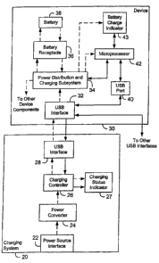
Fig. 2 is a block diagram of. a charging system connected to a device having a
rechargeable power supply. In the charging system 20, the components 22, 24,
26, 27, and 28
are substantially the same as the similarly-labelled components in Fig. 1,
except that the
device power and data interface is a USB interface 27 in Fig. 2. The device
30, as shown,
includes a USB interface 32 to the charging system 20, a power distribution
and charging
subsystem 34, a battery receptacle 36 for receiving a rechargeable battery 38,
a USB port 40,
a microprocessor 42, and a battery charge indicator 43.
The battery 38 supplies power for the device 30 through the power distribution
and
charging subsystem 34. The power distribution and charging subsystem 34
preferably uses
7
CA 02634656 2008-05-30
WO 2004/098020 PCT/CA2004/000663
the power provided by the charging system 20 to both provide operating power
to the device
30 and to charge the battery 38. The particular design of the power
distribution and charging
subsystem 34 is dependent upon the type of the device 30, as will be apparent
to those skilled
in the art, and is substantially independent of the charging status indicator
control scheme
described herein. In the device 30, the power distribution and charging
subsystem 34
provides operating power to the microprocessor 42, the battery charge
indicator 43, and other
device components. A data connection between the microprocessor 42 and the
power
distribution and charging subsystem 34 provides for software-based control and
monitoring
of the power distribution and charging subsystem 34. The microprocessor 42
also determines
a remaining charge level of the battery 38, by monitoring it terminal voltage,
for example,
and provides an indication of battery charge to a user via the battery charge
indicator 43. The
battery charge indicator 43 may include, for example, one or more LEDs or a
user interface
(UI) component that displays an indication of battery charge level on a device
display (not
shown).
Another function of the microprocessor 42, in accordance with an aspect of the
present invention, is to determine charging status of the battery 38 when the
device 30 is
connected to the charging system 20. As described above, the power
distribution and
charging system 34 preferably draws current from the charging system 20 to
both charge the
battery 38 and provide operating power to the device 30. As such, the total
amount of current
drawn by the device 30 can be greater than a normal charging current for the
battery 38 itself,
and the device 30 draws current after the battery 38 is fully charged. This
may cause the
charging controller 26 to control the charging status indicator 26 to provide
a "charging"
indication even though the battery 38 is no longer being charged. Varying
charging current
characteristics between different devices may also introduce errors in
charging status
indication at the charging system 20. The microprocessor 42 or software
executed by the
8
CA 02634656 2008-05-30
WO 2004/098020 PCT/CA2004/000663
microprocessor 42 is configured to determine actual charging status of the
battery 38, by
measuring the charging current being drawn by the battery 38 and comparing the
measured
current against known charging current profile for the device 30, for example,
and to control
both the battery charge indicator 43 and the charging status indicator 27
accordingly.
Operation of the charging system 20 is substantially as described above. When
the
device 30 is connected to the USB interface 28, the charging controller 26
determines
whether the device 30 supports remote control of the charging status indicator
27. In one
embodiment, this determination is based on a predetermined potential or signal
pattern
applied to the USB connection between the USB interfaces 32 and 28 by the
device 30, as
described in further detail below with reference to Fig. 3.
Fig. 3 is a schematic diagram of the USB interface 28 of Fig. 2. It will be
apparent to
those skilled in the art that the Vbus line 44 and the GND line 50 carry power
from the
interface 28 to the interface-32, and the D+-and _ D- data lines--46 and 48
provide the data
connection. The resistors 52 and 54, illustratively 7.5k and 15k ,
respectively, create a
pull-up on the D- data line 48. In order to notify the charging system 20 that
it supports
remote control of the charging status indicator 27, the device 30 momentarily
drives the D-
data line 48 to a low level for a predetermined time when it is connected to
the charging
system 20, and then allows it to return to a high level. These transitions are
detected by the
charging controller 26 and interpreted as an indicator control signal, which
serves to notify
the charging controller 26 that the device 30 supports remote control of the
charging status
indicator 27. Charging status update signals are then provided to the charging
controller 26
to control the charging status indicator 27.
The number and types of charging status update signals provided to the
charging
system 20 depend, for example, on the type of charging status indicator "27
and the USB
interface 28. In a preferred charging status update signalling scheme, the
device 30 pulls the
9
CA 02634656 2008-05-30
WO 2004/098020 PCT/CA2004/000663
D- line 48 to a low level a second time to indicate that the battery 38 is
fully charged. If the
charging status indicator 27 provides multi-level charging status indications,
then additional
charging status update signals may be provided to indicate a present charge
level of the
battery 38, charging time remaining, and the like. It is also possible to
configure the USB
interface 28 to receive charging status update signals via the D+ and D- data
lines 46 and 48.
The data connection between the USB interfaces 28 and 32 is shown in Fig. 2 as
a
one-way connection, with data flowing from the device 30 to the charging
system 20.
However, a two-way data connection may also be desirable, so that the device
30 can also
detect that it has been connected to the charging system 20, for example.
Typically, USB
devices can draw limited current from a USB host. In the case of a charging
system, such a
limit may be undesirable. Therefore, when the device 30 is connected to the
USB interface
28, an identification signal is preferably provided to the device 30 to notify
the device 30 that
itis connected to a power source that is not subject to the normal power
limits imposed by the
USB_ specification. The identification signal also preferably causes the
device 30 to provide
an indicator control signal to the charging system 20.
An identification signal is provided, for example, by the charging controller
26. In a
more "passive" approach, USB interface 28 is configured to provide the
identification signal.
As described above, the resistors 52 and 54 create a slight pull-up on the D-
data line 48.
Although the resistor 56 creates a slight pull-down on the D+ data line 46, D+
is pulled up by
a stronger pull-up at the device 30 when it is connected to the charger 20.
Thus, in this
embodiment, detection of the abnormal data line condition of both D- and D+
being high,.in
most implementations by the microprocessor 42, is interpreted as the
identification signal.
The detection of the identification signal may be accomplished using a variety
of methods.
For example, the microprocessor 42 may detect the identification signal by
detecting the
presence of the above or another abnormal data line condition at the USB port
40. The
CA 02634656 2008-05-30
detection may also be accomplished through the use of other device subsystems
in the device
30. Further details of USB-based charging are provided in the following United
States
Patents 6,936,936 and 6,946,817, both filed on March 1, 2002 and assigned to
the owner of
the instant application.
Referring again to Fig. 3, the resistor 56, connected between the D+ data line
46 and
the GND line 50, results in a pull-down on the D+ data line 46. The stronger
pull-up at the
device 30 pulls D+ high when the device 30 is connected to the charging system
20.
Connection of the device 30 to the charging system 20 can therefore be
detected by detecting
that D+ has been pulled high. Other detection schemes may be apparent to those
skilled in
the art. The present invention is independent of how the connection of a
device to a charging
system is detected.
In response to the identification signal, the device 30 generates the
indicator control
signal and the power distribution and charging system 34 draws power through
Vbus and
GND lines 44 and 50 of the USB interface 28 without waiting for the normal USB
processes
of enumeration or charge negotiation.
The USB connection between the device 30 and the charging system 20 could be
further exploited beyond charging the device 30. For example, the USB
interface 32 may
also be connected to other USB interfaces in other devices or systems, to
support such
extended functions as indirectly powering or charging power supplies in other
devices and
systems through the device 30 through a conventional USB connection. The
device 30 then
provides an interface to another device or power supply that is not itself
compatible with the
charging system 20.
11
CA 02634656 2008-05-30
WO 2004/098020 PCT/CA2004/000663
Fig. 4 is a flow diagram illustrating a charging status indication control
method. The
steps in the method have been described in detail above and are therefore
described briefly
below.
As indicated at 70, a charging status indicator in a charging system is
normally turned
off unless a device is connected to the charging system. Connection of a
device having a
rechargeable power supply is detected at step 72. At step 74, a determination
is made as to
whether the connected device supports remote control of the charging status
indicator, based
on detection of an indicator control signal as described above, for example.
If so, then
charging current is provided to the device, and the charging status indicator
provides a
"charging" indication, at step 76. Steps 78 and 80 respectively illustrate
monitoring for a
charging status update signal and disconnection of the device. In the example
method of Fig.
4, the "charging" indication is maintained until a charging status
update'signal is received, as
-detected -at- step 78, or disconnection of the device is detected- at step
80. When a charging
status update signal indicating that the device power supply has been charged
is received,
charging is complete, and the charging status indicator is controlled to
provide a "charged"
indication at step 82. Disconnection of the device turns the status indicator
off, as shown at
step 70.
Where it is determined at step 74 that the connected device does not support
remote
control of the charging status indicator, charging current is provided to the
device and the
charging status indicator provides a "charging" indication at step 84. The
charging status
indicator is then controlled in a conventional manner, based on the charging
system
determining when the device power supply has been charged, at step 88, or that
the device
has been disconnected, at step 86. Once the device power supply has been
charged, charging
is complete, and the charging status indicator provides a "charged" indication
at step 82.
12
CA 02634656 2008-05-30
WO 2004/098020 PCT/CA2004/000663
The method shown in Fig. 4 and described above is one illustrative example of
a
charging status indicator control method. Modifications of the method are
possible without
departing from the invention.
For example, although only "charging" and "charged" indications are shown, the
charging status control is also applicable to multiple-phase charging cycles,
including a
constant current phase, a constant voltage phase, and a time-limited top-off
charging phase,
for example. A series of charging status update. signals may be provided by a
device and
detected by a charging system to indicate charging cycle status. Multiple
charging status
update signals are also preferred if a charging status indicator can indicate
power supply
charge level or remaining charging time during a charging operation. In other
embodiments
of the invention, multiple charging status update signals are used to toggle
the charging status
indicator between "charged" and "charging" indications.
In addition, the method may revert to one of remote control and conventional
control
responsive to detection of certain conditions. If a device's power supply is
at a very low
charge level, it may be unable to pull down the D- data line when the device
is connected to
the charging system to provide an indicator control signal as described above.
Even though
the device supports remote control of the charging status indicator, it is
unable to notify the
charging system accordingly. However, after the power supply is partially
charged, the
device is able to pull down the line to provide an indicator control signal.
Where the
charging system is configured to monitor the D- data line after charging has
begun, a "late"
indicator control signal can be detected, and the method preferably reverts to
remote indicator
control. In the case of separate power and data interface, the method
preferably reverts to
conventional control if the device is disconnected from the data interface.
Further, although the decision steps 78, 80, 86, and 88 are shown as separate
steps, it
should be appreciated that these steps are preferably monitoring operations
that are performed
13
CA 02634656 2008-05-30
WO 2004/098020 PCT/CA2004/000663
during power supply charging. The charging at steps 76 and 84 need not be
halted to check
for a charging status update signal at step 78 or a power supply charge level
at step 88.
Similarly, detection of disconnection of a device at steps 80 and 86
interrupts the charging at
steps 76 and 84, but the operation of detecting whether a device has been
disconnected, such
as by polling an interface or monitoring for a detection signal, preferably
does not require the
charging to be halted.
Fig. 5 is a block diagram of a wireless mobile communication device, which is
one
type of device for which the charging status indicator control schemes
disclosed herein are
applicable. The wireless mobile communication device ("mobile device") 100 is
preferably a
two-way communication device having at least voice or data communication
capabilities.
Preferably, the mobile device 100 is also capable of communicating over the
Internet, for
example, via a radio frequency ("R.F") link.
The exemplary mobile device 100 comprises a microprocessor 112, a
communication
subsystem 114, input/output ("I/O") devices 116, a USB port 118; and a power
subsystem
120. The microprocessor 112 controls the overall operation of the mobile
device 100. The
communication subsystem 114 provides the mobile device 100 with the ability to
communicate wirelessly with external devices such as other mobile devices and
other
computers. The 1/0 devices 116 provide the mobile device 100 with input/output
capabilities
for use with a device user. The USB port 118 provides the mobile device 100
with a serial
port for linking directly with other computers and/or a means for receiving
power from an
external power source, as described above. The power subsystem 120 provides
the mobile
device 100 with a local power source.
The communication subsystem 114 comprises a receiver 122, a transmitter 124,
antenna elements 126 and 128, local oscillators (LOs) 130, and a digital
signal processor
(DSP) 132. The particular design of the communication subsystem 114 and the
components
14
CA 02634656 2008-05-30
WO 2004/098020 PCTICA2004/000663
used therein can vary. It would be apparent to one of ordinary skill in the
art to design an
appropriate communication subsystem using conventional methods and components
to
operate over a communication network 134 based on the parameters necessary to
operate
over that communication network. For example, a mobile device 100
geographically located
in North America may include a communication subsystem 114 designed to operate
within
the-MobitexTM mobile communication system or DataTACTM mobile communication
system,
whereas a mobile device 100' intended for use in Europe may incorporate a
General Packet
Radio Service (GPRS) communication subsystem 114.
Network access requirements will also vary depending upon the type of network
134.
For example, in the Mobitex and DataTAC networks, mobile devices 100 are
registered on
the network using a unique personal identification number or PIN associated
with each
device. In GPRS networks however, network access is associated with a
subscriber or user of
a mobile device 100. A GPR-S-device therefore requires a subscriber identity
module (not
shown), commonly referred to as a SIM card, in order to operate on a GPRS
network.
Without a SIM card, a GPRS device will not be fully functional. Local or non-
network
communication functions (if any) may be operable, but the mobile device 100
will be unable
to carry out any functions involving communications over the network 134,
other than legally
required functions such as `911' emergency calling.
When required, after the network registration or activation procedures have
been
completed, a mobile device 100 may send and receive communication signals over
the
network 134. Signals received by the antenna element 126 are input to the
receiver 122,
which typically performs such common receiver functions as signal
amplification, frequency
down conversion, filtering, channel selection, and in the exemplary system
shown in Fig. 5,
analog to digital conversion. Analog to digital conversion of a received
signal allows more
complex communication functions such as demodulation and decoding to be
performed in the
CA 02634656 2008-05-30
WO 2004/098020 PCT/CA2004/000663
DSP 132. Similarly, signals to be transmitted are processed, including
modulation and
encoding for example, by the DSP 132 and input to the transmitter 124 for
digital to analog
conversion, frequency up conversion, filtering, amplification, and
transmission over the
communication network 134 via the transmitter antenna element 128. The DSP 132
not only
processes communication signals, but also provides for receiver and
transmitter control. For
example, signal gains applied to communication signals in the receiver 122 and
transmitter
124 may be adaptively controlled through automatic gain control algorithms
implemented in
the DSP 132.
In implementing its device operation control function, the microprocessor 112
executes an operating system. The operating system software used by the
microprocessor
112 is preferably stored in a persistent store such as the non-volatile memory
136, or
alternatively read only memory (ROM) or similar storage element. The
microprocessor 112
may- also -enable the execution-of specific device _-software- applications,
such as a remote
charging status indicator control application or module, for example, which
preferably are
also stored in a persistent store. The operating system, specific device
applications, or parts
thereof, may also be temporarily loaded into a volatile store such as in RAM
138. The non-
volatile memory 136 may be implemented, for example, as a flash memory
component, or a
battery backed-up RAM, for example.
A predetermined set of software applications which control basic device
operations,
including at least data and voice communication applications for example, will
normally be
installed on the mobile device 100 during manufacture. One such application
loaded on the
mobile device 100 could be a personal information manager (PIM) application.
The PIM
application is preferably a software application for organizing and managing
user inputted
data items such as e-mail, calendar events, voice mails, appointments, and
task items. The
PIM data items may be stored in the RAM 138 and/or the non-volatile memory
136.
16
CA 02634656 2011-04-29
The PIM application preferably has the ability to send and receive data items,
via the wireless
network 134. The PIM data items are preferably seamlessly integrated,
synchronized and
updated, via the wireless network 134, with corresponding data items stored or
associated with a
host computer system (not shown) used by the device user. The synchronization
of PIM data
items is a process by which the PIM data items on the mobile device 100 and
the PIM data items
on the host computer system can be made to mirror each other.
There are several possible mechanisms for loading software applications onto
the mobile device
100. For example, software applications may be loaded onto the mobile device
100 through the
wireless network 134, an auxiliary I/O subsystem 140, the USB port 118, a
short-range
communications subsystem 142, such as an infrared ("IR"), Bluetooth, or 802.11
communication
system, or any other suitable subsystem 144. Those skilled in the art will
appreciated
that"Bluetooth"and"802. 11 "refer to sets of specifications, available from
the Institute for
Electrical and Electronics Engineers (IEEE), relating to wireless personal
area networks and
wireless local area networks, respectively.
When loading software applications onto the mobile device 100, the device user
may install the
applications in the RAM 138 or the non-volatile memory 136 for execution by
the
microprocessor 112. The available application installation mechanisms can
increase the utility of
the mobile device 100 by providing the device user with a way of upgrading the
mobile device
100 with additional and/or enhanced on-device functions, communication-
related functions, or
both. For example, a secure communication application may be loaded onto the
mobile device
100 that allows for electronic commerce functions or other financial
transactions to be performed
using the mobile device 100.
The I/O devices 116 are used to accept inputs from and provide outputs to a
user of the mobile
device 100. In one mode of operation, a signal received by the mobile device
100,
17
CA 02634656 2008-05-30
WO 2004/098020 PCT/CA2004/000663
such as a text message or web page download, is received and processed by the
communication subsystem 114, forwarded to the microprocessor 112, which will
preferably
further process the received signal and provides the processed signal to one
or more of the
I/O devices 116 such as the display 146. Alternatively, a received signal such
as a. voice
signal is provided to the speaker 148, or alternatively to an auxiliary 1/O
device 140. In
another mode of operation, a device user composes a data item such as an e-
mail message
using a keyboard 150 in cooperation with the display 146 and/or possibly an
auxiliary I/O
device 140. The composed data item may then be transmitted over -a
communication network
134 using the communication subsystem 114. Alternatively, a device user may
compose a
voice message via a microphone 152, or participate in a telephone call using
the microphone
152 and the speaker 148.
The short-range communications subsystem 142 allows the mobile device 100 to
communicate' with other- systems or devices, which-need not. necessarily be
similar to device
100.-For example, the short-range communications subsystem 142 may include an
infrared
device, a Bluetooth module, or an 802.11 module, as described above, to
support
communications with similarly-enabled systems and devices.
The USB port 118 provides the mobile device 10 with a serial port for linking
directly
with other computers to exchange data and/or to receive power. The USB port
118 also
provides the mobile device 100 with a means for receiving power from an
external power
source. For example, in a personal digital assistant (PDA)-type communication
device, the
USB port 118 could be used to allow the mobile device 100 to synchronize data
with a user's
desktop computer (not shown). The USB port 118 could also enable a user to set
parameters
in the mobile device 100 such as preferences through the use of an external
device or
software application. In addition, the USB port 118 provides a means for
downloading
information or software to the mobile device 100 without using the wireless
communication
18
CA 02634656 2008-05-30
WO 2004/098020 PCT/CA2004/000663
network 134. The USB port 118 provides a direct and thus reliable and trusted
connection
that may, for example, be used to load an encryption key onto the mobile
device 100 thereby
enabling secure device communication.
Coupled to the USB port 118 is a USB interface 154. The USB interface 154 is
the
physical component that couples the USB port to the outside world. In the
exemplary mobile
device 100, the USB interface 154 is used to transmit and receive data from an
external
data/power source 156, receive power from the external data/power source 156,
direct. the
transmitted/received data from/to the USB port 118, and direct the received
power to the
power subsystem 120.
The power subsystem 120 comprises a charging and power distribution subsystem
158 and a battery 160, which have been described above. In conjunction with a
charging
system connected as the data/power source 156, remote control of a charging
status indicator
by-the mobile device 100-in-accordance-with aspects _ of the present invention
is supported.
- This written description may enable those skilled in the art to make and use
embodiments having alternative elements that correspond to the elements of the
invention
recited in the claims. The intended scope of the invention thus includes other
structures,
systems or methods that do not differ from the literal language of the claims,
and further
includes other structures, systems or methods with insubstantial differences
from the literal
language of the claims.
For example, it would be obvious to implement remote charging status indicator
control in a charging system configured to simultaneously charge more than one
device. In
this case, separate charging status indicators are typically provided, and
each is controlled
substantially independently. At any time, each charging status indicator could
be controlled
by either a connected device or the charging system. It is also contemplated
that such a
charging system may incorporate more than one type of device interface,
including interfaces
19
CA 02634656 2008-05-30
WO 2004/098020 PCT/CA2004/000663
with both power and data connections, through which remote charging status
indicator
control is possible, and interfaces with only power connections, for which
corresponding
charging status indicators are controlled by the charging system.
The USB connection shown in Fig. 2 is an illustrative example of one possible
type of
power and data connection between a device and a charging system. Charging
status
indicator control as described herein is not dependent upon any particular
type of connection
or interface, and is adaptable to other types of connections, associated with
integrated
power/data interfaces or separate power and data interfaces. It will also be
apparent that a
data connection is not required where power connection signalling schemes are
implemented.
Where a device and a charging system are configured to detect particular
potential or current
levels on a power connection, a data connection is not necessary.