Note: Descriptions are shown in the official language in which they were submitted.
CA 02637399 2008-07-15
WO 2007/079549 PCT/AU2007/000038
1
DATA STORAGE IN A DIFFRACTIVE OPTICAL ELEMENT
FIELD OF THE INVENTION
This invention relates to data storage and is particularly, but not
exclusively, concerned with data storage in security documents.
BACKGROUND OF THE INVENTION
In security documents such as passports and identification cards it is often
required to store personal data securely on the document. There currently
exist
several data storage mechanisms which have been used in security documents,
including: barcodes, magnetic stripes, optical CD technology contact IC chips
and
contactless IC chips. Each of these data storage devices have some inherent
advantages and disadvantages, but most of them suffer from the disadvantage
that whilst they have the ability to store high volumes of information, the
cost of
producing security documents incorporating such data storage devices is
generally very high.
It is therefore desirable to provide a relatively low cost data storage device
suitable for incorporation into security documents and other articles.
It is also desirable to provide a convenient and relatively inexpensive
method of producing a security document with a data storage device.
SUMMARY OF THE INVENTION
According to a first aspect of the invention there is provided a diffractive
optical element (DOE) comprising a diffractive microstructure which includes
encrypted data physically stored within the microstructure, wherein when the
DOE is illuminated with substantially collimated light, the diffractive
microstructure
generates a far field interference pattern corresponding to the stored data
that is
reconstructed in a reconstruction plane remote from the DOE.
Before the present invention, diffractive optical microstructures, otherwise
known as diffractive optical elements (DOEs), have been used as authentication
devices in security documents such as banknotes. Such a diffractive optical
element, when illuminated with substantially collimated light, generates an
interference pattern which produces a projected visual image when
reconstructed
in the reconstruction plane. However, the use of such DOEs in security
documents for storage of encrypted data other than for producing projected
visual
images has hitherto not been previously proposed.
CA 02637399 2008-07-15
WO 2007/079549 PCT/AU2007/000038
2
According to another aspect of the invention, there is provided a security
document or article which includes a diffractive optical element (DOE) in
accordance with the first aspect of the invention.
The present invention is particularly applicable to diffractive
microstructures known as numerical-type diffractive optical elements (DOEs).
The simplest numerical-type DOEs rely on the mapping of complex data that
reconstruct in the far field (or reconstruction plane) a two-dimensional
intensity
pattern. Thus when substantially collimated light, eg from a point light
source or a
laser, is incident upon the DOE, an interference pattern is generated that
corresponds to the stored data and which may be detected by suitable apparatus
located in the reconstruction plane remote from the DOE. The transformation
between the two planes can be approximated by a fast Fourier transform (FFT).
Thus, complex data including amplitude and phase information has to be
physically encoded in the microstructure of the DOE. This DOE data can be
calculated by performing an inverse FFT transformation of the desired
reconstruction (ie the desired intensity pattern in the far field).
In one preferred embodiment the security document or article incorporating
the DOE is an identification document, and the stored encrypted data in the
microstructure of the DOE includes personalised data relating to the holder of
the
identification document. For example, the identification document could be a
passport, identity card or credit card containing the name and identity number
or
account number of the holder on the document outside the area where the DOE
is provided, with the stored encrypted data in the DOE also containing the
name
and identity or account number of the holder. Thus, the personalised encrypted
data in the DOE provides an additional check for verifying the authenticity of
the
document and deters an unauthorised person from tampering with the
identification document by altering the name or number printed on the card.
The encrypted data may be readable by apparatus 'including a detector
located in the reconstruction plane and ~ decryption means for decrypting the
encrypted data detected by the detector.
The data stored in the DOE may be digitally encoded data or analogue
encoded data. It is possible to encode analogue data in a DOE by using blaze
angle gratings. This has the advantage of being more difficult for an
unauthorised
CA 02637399 2008-07-15
WO 2007/079549 PCT/AU2007/000038
3
person to replicate, but can be more prone to noise when reading the encoded
data.
In one embodiment, the DOE may also be arranged to generate a
projected visual image in the reconstruction plane when the DOE is illuminated
with substantially collimated light. For instance, the projected visual image
may
be an image of the holder of the identification document. The projected visual
image may be generated by a first set of pixels or vector elements in the DOE
and the encrypted data may be stored in a second set of pixels or vector
elements, preferably intertwined with the first set for extra security.
In a particularly preferred embodiment, the diffractive optical microstructure
comprises a plurality of apertures formed in a substantially opaque layer
disposed
on the substrate.
According to another aspect of the invention, there is provided a method of
storing and reading data in a document including the steps of:
providing , a diffractive optical microstructure in the document wherein
encrypted data is stored in the microstructure;
illuminating the diffractive optical microstructure with substantially
collimated light whereby a far field interference pattern is generated
corresponding to the encrypted data that is reconstructed in a reconstruction
plane remote from the diffractive optical microstructure;
detecting the far field interference pattern in the reconstruction plane; and
decrypting the encrypted data detected in the interference plane.
The far field interference pattern generated by the diffractive optical
microstructure is preferably detected by detecting the light intensity of the
interference pattern in the reconstruction plane. The encrypted data in the
light
intensity pattern may then be decrypted by a computer program which transforms
the detected light intensity pattern into machine readable data.
According to a further aspect of the invention, there is provided apparatus
for reading encrypted data stored in a diffractive optical microstructure in a
document including:
means for directing a substantially collimated beam of light onto the
diffractive optical microstructure such that the beam is transformed into a
far field
CA 02637399 2008-07-15
WO 2007/079549 PCT/AU2007/000038
4
interference pattern corresponding to the stored encrypted data that is
reconstructed in a reconstruction plarie remote from the microstructure;
optical detection means located in the reconstruction plane for detecting
the far field interference pattern and for generating 'signals representing
the
stored encrypted data; and
processing means for receiving and processing the signals from the optical
detection means, wherein the processing means includes decryption means for
decrypting the encrypted data represented by the signals from the detection
means.
In various embodiments of the invention, a variety of different approaches
may be taken for forming the diffractive optical microstructure on the
substrate or
in a layer applied thereto. In one general class of processes according to
embodiments of the invention, a layer is applied to the substrate, and the
diffractive optical microstructure is formed by a plurality of apertures in
this layer
eg by ablation. Additional layers may be applied to the substrate either
before or
after ablation, ie the diffractive optical niicrostructure may be formed in a
surface
layer, or in an internal layer of a plurality of layers applied to the
substrate.
In some embodiments of the invention, the layer applied to the substrate is
an opacifying layer, whereby a transmissive diffractive optical microstructure
is
formed by ablation of apertures in the opacifying layer.
In another general class of processes according to embodiments of the
invention, the diffractive optical microstructure is formed by ablation of the
surface
of the substrate itself. Following ablation, the surface may be coated with a
reflective film, to produce a diffractive optical structure that is visible in
reflection
through the transparent substrate. Alternatively, the surface may be left
uncoated, or be coated with a transparent coating having a different
refractive
index to that of the substrate. According to this method, a diffractive
optical
element can be formed that is visible in transmission through the document,
when
illuminated using a point light source, such as a visible laser, projected
onto a
suitable viewing surface.
Furthermore, in accordance with embodiments of the invention various
means and methods may be employed to ablate a layer applied to the substrate,
or to ablate the surface of the substrate itself.
CA 02637399 2008-07-15
WO 2007/079549 PCT/AU2007/000038
One general ablation process applicable to embodiments of the invention
is laser ablation, involving the exposure of one or more areas of the
substrate, or
layer applied thereto, to laser radiation in order to form a three dimensional
optically diffractive structure therein, or to ablate apertures in an opaque
layer.
5 According to preferred embodiments, laser ablation may be performed by
direct laser scanning of the desired personalised diffractive optical
microstructure
onto the surface of the substrate or layer applied thereto. Advantageously,
direct
laser scanning includes the individualised control of a laser beam, such as by
the
use of computer numerical control (CNC), in order to form an individual or
unique
optical microstructure.
Alternatively, laser ablation may be performed by first forming a
personalised mask corresponding with the desired personalised diffractive
optical
microstructure using appropriate methods in accordance with embodiments of the
invention, and then exposing the substrate, or layer applied thereto, to laser
radiation directed through the mask. The mask may be designed such that the
substrate or layer is exposed in the near field to laser radiation directed
through
the mask, whereby the mask includes apertures substantially formed in the
shape
of the desired areas to be ablated. Alternatively, the mask may be designed
such
that the substrate or layer is exposed in the far field to laser radiation
directed
through the mask, whereby the mask includes apertures formed to produce a
diffraction pattern corresponding with the shape of the desired areas to be
ablated.
Advantageously, the mask may be manufactured to a larger scale than the
desired diffractive optical microstructure, which is subsequently created by
exposure of the substrate or layer applied thereto by reducing optics, such as
a
suitable lens arrangement. Advantageously, this approach increases the
required
minimum feature size of the mask, thereby enabling the use of lower precision
equipment for the formation of the mask. Furthermore, the mask may be
generated in cheap materials, such as aluminium coated polypropylene. In
addition, the durabiiity of the mask may be improved due to the reduced
required
optical power density instant upon the mask. All of the aforementioned factors
may reduce the cost and complexity of mask production, thereby enabling
individually personalised masks to be produced for use in forming
corresponding
CA 02637399 2008-07-15
WO 2007/079549 PCT/AU2007/000038
6
personalised diffractive optical microstructures within acceptable timeframes
and
at acceptable costs.
In this regard, masks may generally be made by a variety of methods,
including, but not limited to, the various techniques disclosed herein for
forming
optical structures in opaque layers disposed on the surface of transparent
substrates.
In particularly preferred embodiments, the method involves generating a
mask in parallel with the manufacture of other features and elements of the
security document or article, thereby further reducing the overall time
required to
manufacture the final security document or article.
According to one preferred method in accordance with the invention, the
desired diffractive optical microstructure is represented as an array of
discrete
elements. In a particularly preferred embodiment, the diffractive optical
microstructure is represented as a two dimensional field having predetermined
dimensions, and the method includes:
subdividing the two dimensional field into an array of discrete elements;
and
determining the content -of discrete elements of the field in order to form
the stored data of the diffractive optical microstructure.
Each discrete element may be a square or rectangular pixel, and
accordingly the data may be stored in the diffractive optical microstructure
as a
bitmap. The resulting bitmap may be used for direct laser scanning of the
substrate, for example using an XY galvanometer or a CNC stage to scan a laser
over the substrate whereby the laser is activated to ablate points on the
substrate
or layer applied thereto corresponding with discrete elements or pixels of the
bitmap. The laser used for this process may be, for example, a frequency
tripled
or quadrupled Nd:YAG system with a telecentric scanning head, providing a
pixel
size of typically 7 microns. Alternatively, a CNC stage may be used in
conjunction with a frequency doubled Nd:YAG laser, providing typically a
smaller
pixel size of 5 microns or less.
In other embodiments, instead of representing the diffractive optical
microstructure as an array of discrete elements, the microstructure may be
represented as a plurality of narrow vector elements or tracks. According to
CA 02637399 2008-07-15
WO 2007/079549 PCT/AU2007/000038
7
methods of this type, each track is sufficiently narrow to cause diffraction
of light
passing therethrough. The tracks may be straight, curved or of arbitrary shape
in
accordance with the requirements of the desired diffractive optical
microstructure.
The method may then include:
generating a diffractive optical microstructure mask image; and
converting the diffractive optical microstructure mask image into a plurality
of vectors corresponding with the narrow tracks. This conversion to form a
representation of the diffractive optical microstructure as a plurality of
narrow
tracks may be performed digitally upon a bitmap image of the diffractive
optical
microstructure mask using image analysis techniques known in the art.
A particular advantage of embodiments based upon a diffractive optical
microstructure represented as a plurality of narrow tracks is that a laser
having a
relatively large spot size may be used to generate the corresponding mask. For
example, track widths of 20 to 25 microns may be used to produce diffractive
optical microstructures substantially equivalent to those produced from bitmap
images having a pixel size of around 10 microns. As with previously described
embodiments, direct laser scanning using an XY galvanometer or a CNC stage
may be used to generate a suitable mask from the representation based upon a
plurality of narrow tracks.
In still further embodiments, the diffractive optical microstructure may be
represented as a tiled array of square or rectangular sub-regions, each
corresponding with, for example, a group of pixels. In preferred embodiments,
each sub-region may correspond with an area of around 10 to 20 pixels wide by
10 to 20 pixels high. Preferably, each sub-region is approximated by one of a
predetermined plurality of masks, each mask defining a fixed graphical form,
for
example, a curve, a verticai line, a horizontal iine, and/or a line arranged
along a
diagonal or at any arbitrary angle relative to the sub region.
A desired personalised diffractive optical microstructure, or a mask for
forming such a diffractive optical microstructure, may then be constructed by
exposing the sub-regions of the substrate or layer applied thereto to laser
radiation through corresponding masks selected from the predetermined
plurality
of masks.
CA 02637399 2008-07-15
WO 2007/079549 PCT/AU2007/000038
8
In a representative embodiment, a library of around 100 masks or fewer
may be provided representing various possible configurations of each square or
rectangular sub-region of the tiled array representing the diffractive optical
microstructure. In a particularly convenient arrangement, the library of masks
may be formed on a single plate, such as a quartz mask plate, positionable to
expose the corresponding sub-regions of the representation in accordance with
the desired diffractive optical microstructure. Advantageously, embodiments of
the invention based upon representing the diffractive optical microstructure
as a
tiled array of sub-regions may result in a considerable reduction in the
formation
time of the microstructure, by comparison with individual pixel writing
methods.
For example, a 4 to 16 million pixel mask may be reduced to only 20,000 sub
regions which, at 200 Hz, may be formed in around 100 seconds.
In yet further embodiments, a personalised diffractive optical
microstructure may be formed by direct imaging including the step of directing
a
laser beam onto the substrate, or layer applied thereto, using a micro-mirror
array. Such an array may consist of a very large number, for example millions,
of
individual micro-mirrors, each of which may be controlled electronically in
order to
direct the reflective face of the mirror at a desired angle. In preferred
embodiments, the angle of each mirror is set either to direct light onto, or
away
from, the substrate or layer, in order to generate a pattern of illumination
corresponding with the diffractive optical microstructure to be formed
thereon.
In one advantageous arrangement, the light directed away from the
substrate by the mirrors may be directed at a second target, such as a further
similar substrate, in order to generate a second identical diffractive optical
microstructure on the second target using the same laser pulse. As will be
appreciated by those skilled in the art, the inverse of a mask for forming a
diffractive optical microstructure produces a structure having identical
optical
imaging properties to the original, uninverted, mask.
In variations of this method, multiple smaller beams may be used in
combination with smaller and simpler micro mirror arrays in order to generate
a
diffractive optical microstructure using patterns of interference between said
beams.
CA 02637399 2008-07-15
WO 2007/079549 PCT/AU2007/000038
9
Yet another alternative method of producing a personalised diffractive
optical microstructure includes providing at least two masks, each of which
may
again be selected from a library of masks, each thereby corresponding with a
predetermined diffractive element. The step of forming the diffractive optical
microstructure on the substrate or layer applied thereto may then include
exposing the substrate or layer to laser radiation directed through each one
of
said masks. In accordance with this method, a diffractive optical
microstructure is
produced which is a superposition of the diffractive elements corresponding
with
the masks. When suitably illuminated, such as with a substantiaily collimated
beam of light, an image is generated which includes sub-images corresponding
with each of the constituent diffractive elements. Accordingly, personalised
diffractive optical microstructures may be formed from unique combinations of
selected masks, or from combinations of masks that are specific to a
particular
individual. For example, a library of masks corresponding with generated
images
of alphanumeric characters may be provided, and diffractive optical
microstructures formed from superimposed combinations of two such masks,
corresponding with the initials of a particular individual. The superposition
of
diffractive elements may be performed, in various embodiments, either by
simultaneous or sequential exposure of the substrate, or layer applied
thereto, to
laser radiation directed through the masks.
In still further embodiments of the invention, methods other than direct
laser writing may be used to form diffractive optical microstructures
containing
stored data and/or to form masks suitable for the creation of diffractive
optical
microstructures by laser writing methods.
For example, according to one such embodiment a diffractive optical
microstructure or a mask may be formed by printing the required pattern onto a
suitable transparent substrate. Preferably, a printing technique is employed
that
is capable of providing a true resolution of 5,000 dpi, thereby producing
printed
pixels on the mask having dimensions of around 5 microns. It will be
appreciated
that the term "true resolution" is intended to refer to the actual pixel size,
and not
to the density of ink spots printed, to which the specification of printing
resolution
often relates. That is, printing techniques compatible with embodiments of the
invention must deposit toner or ink elements of a sufficiently smaller size
for the
CA 02637399 2008-07-15
WO 2007/079549 PCT/AU2007/000038
formation of a diffractive optical microstructure mask, and not merely provide
printed elements of a high density.
In further embodiments of the invention, a direct mechanical process may
be used to form a diffractive optical microstructure and/or a mask for the
5 production of a diffractive optical microstructure. According to some
embodiments of this type, a CNC stage may be fitted with one or more
mechanical ablating structures, such as needles, which may be used to
selectively physically remove layers of coating from a substrate, such as by
scraping. Layers may be mechanically removed in this manner from the
10 substrate itself, or from a photoresist or other layer disposed on the
surface of the
substrate for this purpose. According to preferred embodiments, a diffractive
optical microstructure of a corresponding mask is thereby formed through the
operation of an XY scanning system controlling the needles in order to
mechanically ablate individual elements or pixels, or alternatively to ablate
narrow
tracks or vectors.
Yet further embodiments of the invention may employ electro-chemical
machining for the formation of diffractive optical microstructures and/or
masks for
use in the production of diffractive optical microstructures. According to a
method
of electro-chemical machining, portions of a metal layer are removed from a
substrate using an electrical current in a suitable salt solution. An
electrode is
preferably provided which is shaped to correspond with the areas of the metal
layer that are to be removed from the substrate. According to one embodiment,
a
reconfigurable electrode is formed as an array of individual electrode
elements,
such as pins, selectably extensible or retractable to generate a desired
diffractive
optical microstructure pattern, in the manner of an array of pixels. Such an
electrode may be used to form a desired pattern, and to image the pattern onto
metalised quartz or polymer, whereby the resulting mask may be used for the
formation of a diffractive optical microstructure using laser writing
techniques.
As will be appreciated from the foregoing summary, methods in
accordance with the present invention provide practical time and cost
effective
processes for the formation of diffractive optical microstructures containing
stored
date on security documents and/or other articles. In accordance with the
invention, limitations of the prior art whereby it is generally practical only
to mass
CA 02637399 2008-07-15
WO 2007/079549 PCT/AU2007/000038
11
produce predetermined diffractive optical micro structures are mitigated,
thereby
enabling the practical realisation of unique, secure documents with stored
data.
In one preferred method, the stored data may be encrypted before the
diffractive optical microstructure is created. Alternatively, the data may be
encrypted during a Fourier transforrri calculation for the creation of the
diffractive
optical microstructure.
Another preferred method may include the step of storing a visual image in
the diffractive optical microstructure such that when suitably illuminated a
projected visual image, such as a personalised image, is generated which is
viewable in the reconstruction plane. Parts of the diffractive optical
microstructure
representing the encrypted data may be intertwined with parts of the
microstructure representing the visual image for extra security.
In another aspect, the present invention provides a personalised security
document or article which includes:
a substrate which is transparent at least to visible light; and
a diffractive optical microstructure formed on the substrate or in a layer
applied thereto, using any one of the method's hereinbefore described.
BRIEF DESCRIPTION OF THE DRAWINGS
Preferred embodiments of the present invention will now be described, by
way of example only, with reference to the accompanying drawings, in which:
Figure 1 is a plan view of an identification card incorporating a diffractive
optical element in accordance with an embodiment of the invention;
Figure 2 is a schematic view on the line I1-II of Figure 1;
Figure 3 is an enlarged schematic view of the diffractive optical element of
Figure 1;
Figure 4 is a schematic view of apparatus for detecting data stored in a
diffractive optical element in a document.
Figure 5 is a schematic view of apparatus for detecting data stored in a
diffractive optical element in a modified document;
Figure 6 is a block diagram of apparatus for reading encrypted data stored
in a diffractive optical element;
CA 02637399 2008-07-15
WO 2007/079549 PCT/AU2007/000038
12
Figure 7 is a schematic view illustrating a method of producing a diffractive
optical element with stored data in accordance with an embodiment of the
invention;
Figure 8 is a schematic view of another method of producing a diffractive
optical element with stored data;
Figure 9 is a schematic view of a further method of producing a diffractive
optical element with stored data;
Figure 10 is a schematic section through an identification card
incorporating a diffractive optical element with stored data;
Figure 11 illustrates an apparatus for performing a method of direct laser
scanning using an XY galvanometer according to an embodiment of the
invention;
Figure 12 illustrates an apparatus for performing a method of direct laser
scanning using a CNC stage according to an embodiment of the invention;
Figure 13 illustrates an example of pixel marking of a substrate according
to an embodiment of the invention;
Figure 14 illustrates an example of vector scanning of a substrate
according to an embodiment.of the invention;
Figure 15 illustrates an example of sub-region masks for a method of
scanning mask ablation according to an embodiment of the invention.
Figure 16 illustrates apparatus for performing a method of scanning mask
ablation according to an embodiment of the invention;
Figure 17 illustrates apparatus for performing a method of direct imaging
using a micro-mirror array according to an embodiment of the invention;
Figure 18 illustrates apparatus for performing a method of direct CNC
machining according to an embodiment of the invention; and
Figure 19 illustrates apparatus for performing a method of electro-chemical
machining according to an embodiment of the invention.
DETAILED DESCRIPTION OF PREFERRED EMBODIMENTS
Referring to Figures 1 and 2 there is shown a security document in the
form of an identification card 1 incorporating a personalised diffractive
optical
element 5 in accordance with the invention. The identification card 1 is
formed
from a transparent substrate 2 of polymeric material such as a laminate
including
CA 02637399 2008-07-15
WO 2007/079549 PCT/AU2007/000038
13
at least one layer of biaxially oriented polypropylene. One or more opacifying
layers 3 are applied to opposite surfaces of the substrate 2 in such a manner
as
to form a transparent window 6 in an area of the substrate 2 which is
uncovered
by the opacifying layers 3. The personalised diffractive optical element 5 is
provided in the transparent window 6.
While the identification card 1 illustrated in Figures 1 and 2 incorporates a
transmissive diffractive optical element formed by ablation of a surface of
substrate 2, this embodiment is provided by way of example only, and a variety
of
methods and structures may be employed for providing a diffractive optical
element within a security document or other article. For example, a
transmissive
or reflective diffractive optical element may be provided by the application
and/or
ablation of additional transparent or reflective layers to the substrate, such
as
described hereafter with reference to Figure 7. Alternatively, a transmissive
diffractive optical element may be provided by ablating apertures in an opaque
layer applied to the substrate, such as described hereafter with reference to
Figures 8 to 10. Various methods suitable for forming these and other
diffractive
structures are described herein, by way of example, with reference to Figures
11
to 19.
In one embodiment, the opacifying layers 3 may be formed from a
pigmented coating containing titanium dioxide, and information 40, such as the
card number, the name of the card holder may be printed and/or embossed on
the opacifying layers. As shown in Figure 1 a photograph 4 of the card holder
is
also provided on the opacified portion 9 of the card 1.
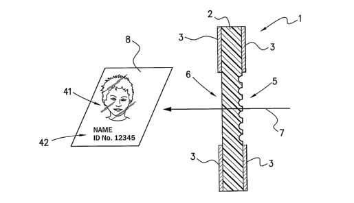
As shown in Figure 2, the personalised diffractive optical element 5 is a
diffractive microstructure in the form of a numerical-type diffractive optical
element
(DOE) which when illuminated by a beam of substantially collimated light 7, eg
from a point light source or laser, generates an interference pattern that
produces
a projected image 41 in a reconstruction plane that is visible when a viewing
surface, such as a sci-een 8 is located in the reconstruction plane. The
projected
image 41 shown in Figure 2 includes an image of the card holder corresponding
to the photograph 4 of the card holder on the opacified portion of the card 1.
Thus, in the event of tampering with the card to remove, alter or replace the
photograph 4 of the card holder, it is possible to detect that the card has
been
CA 02637399 2008-07-15
WO 2007/079549 PCT/AU2007/000038
14
tampered with by comparing the projected image 41 with the photograph 4 on the
card itself.
In accordance with embodiments of the invention, the DOE 5 also includes
data stored within its diffractive microstructure. The data may include
alphanumeric data, such as the personal details of the card holder, eg the
card
holders name and identification or account number 42 which may be viewed on
the viewing screen B in the reconstruction plane as illustrated in Figure 2.
Additionally, the data stored in the microstructure of the DOE 5 includes
encrypted information which requires appropriate decryption apparatus for
reading the encrypted data.
Referring to the schematic enlarged view of the DOE 5 in Figure 3, the
DOE 5 has a central diffractive zone 50 and an array of smaller diffractive
pixel
elements 51 each of which can store individual bits of information. In
conventional DOEs, the central diffractive zone 50 and the pixel elements 51
correspond to different parts of the projected image 41 produced on viewing
screen B in the reconstruction plane by the interference pattern generated
when
the DOE 5 is illuminated with substantially collimated light. A typical DOE
for
producing projected visual images may be located within a 75x75 pm (micron)
square and can contain up to 3025 (55x55) pixels.
In contrast to conventional DOEs for producing projected visual images, at
least some of the pixels 51 of the DOE are used to store encrypted data, and
may
additionally include further data other than visual images, such as
alphanumeric
data. It will be appreciated that if the size of the DOE is increased, eg to a
30mmx3Omm square, the number of pixels is greatly increased. For example, in
a 30mmx30mm square DOE, it is possible to store about 57Mb of information,
without redundancy.
When the data stored in the DOE is encrypted, apparatus for reading the
encrypted data is required, as illustrated schematically with reference to
Figures 4
to 6.
Figure 4 shows apparatus for reading encrypted data from document 10
incorporating a diffractive optical element (DOE) 11 provided in a transparent
portion or window 12 of the document 10. The apparatus comprises a point light
CA 02637399 2008-07-15
WO 2007/079549 PCT/AU2007/000038
source 14 which directs an incident beam of substantially collimated light 15
onto
the DOE 11, and detection means in the form of an optical detection device 16.
In one preferred embodiment, the document 10 may be formed from an at
least partially transparent substrate having one or more opacifying layers or
5 coatings applied to at least one face of the substrate. The transparent
portion or
window 12 of the document 10 may be formed by applying the opacifying layers
or coatings to the substrate in such a manner that the substrate 12 is
substantially
free of opacifying layers or coatings in the region of the transparent portion
or
window 12. The transparent substrate may be formed from a transparent
10 polymeric material, such as polyethylene (PE), polypropylene (PP) or
polyethylene terephthalate (PET). In the case of security document such as a
banknote, the substrate is preferably formed from at least one biaxially
oriented
polymeric film. The substrate may comprise a single film of polymeric
material.
Alternatively, the substrate may comprise a laminate of two or more layers of
15 transparent biaxially oriented polymeric film.
It will, however, be appreciated that the present invention is equally
applicable to documents formed from paper or other partially or fully opaque
material, In this case, an aperture may be formed in the paper or other
material
and a patch of transparent polymeric material inserted into or applied over
the
aperture to form the transparent portion or window 12.
The opacifying layers may comprise one or more of a variety of opacifying
inks which can be used in the printing of banknotes or other security
documents.
For example, the layers of opacifying ink may comprise pigmented coatings
comprising a pigment, such as titanium dioxide, dispersed within a binder or
carrier of cross-linkable polymeric material.
The diffractive optical element (DOE) 11 acts to transform the incident light
beam 15 from the point light source 14 as the beam passes through the at least
partially transparent portion 12 of the security document (the window created
through the security document) into an interference pattern 17. The DOE 11 is
a
complicated surface micro relief structure which includes encrypted data
stored in
its pixels. Whilst the optical transformation of the incident light beam 15 to
the
interference pattern 17 is based on the optical principle of diffraction, the
mathematics of the structure of such devices is specifically designed in each
case
CA 02637399 2008-07-15
WO 2007/079549 PCT/AU2007/000038
16
to produce a distinct optical transformation so that the encrypted data is
detected
by the optical detector 16 is in a reconstruction plane located at a
particular point
in space away from the document 10. The location of the optical detector 16
can
be dependent on the wavelength of the light beam used.
The point light source 14 for producing the incident beam 15 may comprise
an LED, a halogen light source, a laser or other light source for producing a
beam
of substantially collimated light which is directed on the DOE 11.
The optical detection device 16 is position at the particular reconstruction
plane in space at which the interference pattern 17 containing the stored data
is
reconstructed by the DOE 11.
The presence of the encrypted data stored and projected by the DOE 11 is
determined by the amplitude of the response of the detector 16 at particular
points in space where the detector is located. For this purpose, the detector
may
comprise an array of photo-diodes 18, or a charge couple device (CCD) such as
a line CCD or a matrix CCD.
Figure 5 shows a modified embodiment which is similar to Figure 4 and
corresponding reference numerals have been applied to corresponding parts.
The document 20 in Figure 5 differs from that of Figure 4 in that the
transparent
portion or window 12 incorporates a reflective surface 21 underneath the
diffractive optical projection element (DOE) 11. The reflective surface may be
provided by a metallic layer 22 provided within the window 12 or by a
metallised
coating applied to a surface of the transparent portion forming the window 12
before the DOE 11 is applied over the reflective surface 21.
The apparatus of Figure 5 also differs from that of Figure 4 insofar as the
point light source 24 and the optical detector 26 are located on the same side
of
the document 20. The light source 24 is arranged to direct a substantially
collimated incident beam 15 onto the window 12 at an acute angle to the
perpendicular to the surface of the security document 20 so that the incident
beam 15 is reflected back from the reflective surface 21 of the metallic layer
22
onto the DOE 11. The reflected beam passes through the DOE 11 and is
transformed by the DOE 11 into an interference pattern 17 in similar manner to
the embodiment of Figure 1.
CA 02637399 2008-07-15
WO 2007/079549 PCT/AU2007/000038
17
The detector 26, which may also comprise an array of photo-diodes 18 or
a line or matrix CCD, is disposed at a position relative to the security
document
20 to receive the patterned beam 17 which also travels from the DOE 11 at an
acute angle to the perpendicular to the surface of the security document 20
corresponding to the angle of the incident beam 16. Otherwise, the detector 26
functions in exactly the same manner as the detector of Figure 1 by
determining
the amplitude of different parts of the reconstructed projected data formed by
the
interference pattern 17 at particular points in space in the reconstruction
plane
where the photo-diodes 18 are located.
In an alternative embodiment similar to Figure 2, the light source 24 is
arranged to direct the substantially collimated incident beam at an acute
angle
onto the DOE 11 which transforms the beam into an interference pattern 17 that
is reflected by the reflective surface 22 and projected onto the detector 26
located
in the reconstruction plane at the particular position in space where the data
is
reconstructed by the interference pattern 17. It is also possible that the DOE
could be viewed in reflection without an underlying metallic surface using the
reflectivity of the polymer surface.
Figure 6 illustrates a processing apparatus and method of reading
encrypted data utilizing the detection apparatus of Figure 1 or Figure 2.
The equipment of Figure 6 comprises an edge detector 30 for detecting the
presence of a security document, such as an identification card, a window
locator
32 for locating a window 12 in a security document incorporating a DOE 11, an
optical detector 16, 26 in the form of a CCD or photo-diode array for
detecting an
interference pattern 17 generated by the DOE 11, a processor 34 for processing
and analysing signals from the optical detector 16, a decoder for decrypting
encrypted data signals from the processor, 34, and a visual display 38 for
displaying the data decrypted by the decoder 36.
A preferred method of operation of the apparatus of Figures 4 to 6 will now
be described. When a security document 10, 20 such as an identification card,
enters the apparatus the edge detector 30 detects the presence of the document
to activate the window locator 32. When the window locator 32 locates a window
12 in the document 10, 20, the light source 14, 24 and the CCD or photodiodes
CA 02637399 2008-07-15
WO 2007/079549 PCT/AU2007/000038
18
array 18 of the optical detector 16, 26 are activated, eg by means of a time-
gated
output from the processor 34.
The optical detector 16, 26 then detects the light intensity of the
interference pattern 17 generated by the diffractive optical element (DOE) 11
at
the reconstruction plane where the CCD or diode array 18 is located and
produces output signals corresponding to the encrypted light intensity data
stored
in the DOE 11. These signals representing the encrypted data are input to the
processor 34 which analyses the signals. The processor 34 may comprise a
process logic chip (PLC) or a microprocessor, such as a PLC chip which
transforms the signals into machine readable data signals. The signals
transformed by the processor 34 are decrypted by decoder 36 and then the
decrypted information can be displayed on the VDU 38.
A diffractive optical element (DOE) including stored data in the form of
alphanumeric and/or encrypted data may be made by a variety of methods, some
of which are described with reference to Figures 7 to 15.
Referring to Figure 7, there is provided a substrate 2 of transparent
polymeric material (Figure 7a) to which a transparent coating 60 is applied
(Figure 7b). A mask 64 containing apertures 65 corresponding to the
diffractive
optical microstructure for the DOE is placed in front of the substrate 2 and
the
transparent coating 60 is irradiated with laser radiation through the mask 65
to
form the diffractive optical microstructure 61 of the DOE by laser ablation of
the
transparent coating 60 as illustrated by Figure 7c.
The diffractive optical microstructure of the DOE formed in the transparent
coating 60 applied to the substrate 2 may be used as a transmissive DOE
continuing alphanumeric and/or encrypted data in similar manner to that
illustrated by Figures 2 and 4. In a modified embodiment (not shown), the
diffractive optical microstructure 5 may be formed by laser ablation directly
in the
surface of the substrate 2 of transparent polymeric material as shown in
Figure 2.
In another embodiment shown in Figure 7d, a reflective coating 62, eg of
metallic material, may be applied over the transparent coating 60 to form a
reflective DOE 66 containing alphanumeric or encrypted data which may be used
in similar manner to that of Figure 5.
CA 02637399 2008-07-15
WO 2007/079549 PCT/AU2007/000038
19
An alternative method of producing an article, such as an identification
card, with a DOE containing stored alphanumeric and/ or encrypted data is
illustrated by Figure 8.
In Figure 8, there is shown a transparent plastics film 70 formed from
polymeric material, used in the manufacture of a security document, or similar
article, such as an identity card. The substrate 70 may be made from at least
one
biaxially oriented polymeric film. The substrate 70 may include or consist of
a
single layer of film of polymeric material, or, alternatively, a laminate of
two or
more layers of transparent biaxially oriented polymeric film. The substrate 70
is
shown in cross section in Figure 8a.
An opacifying layer 72 is applied to one surface of substrate 70 (Figure
8b). The opacifying layer 72 may include any one or more of a variety of
opacifying inks suitable for use in the printing of security documents formed
from
polymeric materials. For example, the layer of opacifying ink 72 may include
pigmented coatings having a pigment, such as titanium dioxide, disbursed
within
a binder or carrier of heat activated cross-linkable polymeric material.
Laser radiation, in the form of laser beam 76, is then directed onto a mask
74 that is interposed in the path of the laser radiation (Figure 8c). Mask 74
has
apertures, eg 75, through which the laser radiation passes. The passing of the
laser radiation through the apertures of the mask 74 results in the formation
of a
patterned laser beam 78 which bears a pattern corresponding with the desired
diffractive structure in accordance with the mask 74.
In accordance with the embodiment illustrated in Figure 8, the patterned
laser beam 78 passes through transparent substrate 70 and irradiates
opacifying
layer 72. The wavelength of the laser radiation, and the polymeric material
used
to form substrate 70, are selected such that the substrate 70 is substantially
transparent to the laser radiation. Accordingly, the patterned laser beam 78
is
able to pass through substrate 70 with little or no absorption of the
radiation, and
therefore little or no heat build up and subsequent damage to the substrate,
to
impinge upon opacifying layer 72. In the preferred embodiment, the substrate
is
formed of biaxially oriented polypropylene (BOPP) and the wavelength of the
laser radiation used is approximately 248nm, derived from an excimer laser
source.
CA 02637399 2008-07-15
WO 2007/079549 PCT/AU2007/000038
The opacifying layer 72 is a relatively strong absorber of laser radiation at
the selected wavelength, and therefore the patterned laser radiation is
absorbed
in opacifying layer 72, resulting in particies of opacifying layer 72 being
ablated in
accordance with the pattern of laser beam to form apertures 80 in the
opacifying
5 layer (Figure 8d).
The apertures 80 form the optically diffractive microstructure of the DOE
82. Visible light emitted from a point source on one side of opacifying layer
70
will pass through apertures 80, but be blocked by the remaining, unablated
opacifying ink layer 72. A diffraction pattern containing alphanumeric and/or
10 encrypted data will thus be formed in the transmitted light, which is
reconstructed
in a reconstruction plane remote from the DOE. The data stored is determined
by
the pattern of ablated portions 110, which is in turn determined by the
pattern of
apertures in mask 104. Accordingly, by forming an appropriate mask, a
diffractive
structure 112 may be created corresponding to any desired data.
15 Subsequent to forming the diffractive optical structure 82, a further
protective layer 84 may be applied over the structure (Figure 8e). The
protective
layer may be, for example, a protective varnish coating, or a further
transparent
laminate. The protective layer 84 will fill the ablated regions 80 in the
opacifying
layer 72, however since the diffractive optical structure 82 relies upon
20 transmission of light through the ablated portions rather than on a change
in
refractive index, such filling of the ablated regions does not result in the
destruction of the diffractive microstructure.
Turning now to Figure 9, there is shown an alternative embodiment of the
invention, in which a transparent plastics substrate 70 formed from polymeric
material has been coated with opacifying layer 72. Focussed or collimated
laser
beam 86 is directed onto opacifying layer through transparent substrate 70. By
the same processes previously described with reference to Figure 8, laser beam
86 passes through transparent substrate 70 and impinges upon opacifying layer
72 causing ablation of the opacifying layer to remove a selected portion 90.
Laser beam 86 is preferably emitted from a scribe laser (not shown), which
may be controiled to inscribe any desired pattern of ablated regions in
opacifying
layer 72. Accordingly, the scribe laser may be controlled so as to produce any
desired diffractive microstructure 92 in opacifying layer 72.
CA 02637399 2008-07-15
WO 2007/079549 PCT/AU2007/000038
21
Through the use of a scribe laser, an individual diffractive structure 92 may
be formed in opacifying layer 72. In accordance with this embodiment of the
invention, therefore, personalised security documents, such as identification
cards, may be produced with alphanumeric and/or encrypted data, that are
unique to a particular individual.
Again, a further protective layer 94 may be applied over the diffractive
microstructure 92, filling the ablated regions, without destroying the
diffractive
properties of the structure.
Figure 10 illustrates schematically, in cross-section, one embodiment of a
completed security document made in accordance with the method of the
invention. In producing the completed article, transparent substrate 70
preferably
formed from biaxially oriented polypropylene (BOPP) is coated with opacifying
layer 72, and diffractive microstructure 82, 92 ablated from the opacifying
layer in
accordance with an embodiment of the method of the invention as described with
reference to Figure 8 or Figure 9.
Once the optically diffractive structure 82, 92 has been produced, further
layers may be applied in order to complete the article. In the embodiment
shown
in Figure 10, a further supporting layer 96 has been applied. Subsequently,
an,
additional layer of a biaxially oriented polymeric material 98 has been
applied,
and further protective laminates 99 have been applied as an overlay on each
side
of the article.
Since the diffractive optical microstructure 82, 92 is formed prior to the
application of further layers, the supporting layer 96 may be formed from
stiffer
materials that are more suitable for forming identity cards, credit cards or
the like,
but which are not transparent to the wavelength of laser light used to ablate
the
selected portions of the opacifying layer 72. For example, supporting layer 96
may be a polyethylene/polyester coextrusion, which is not transparent to light
having a wavelength of 248nm. It will, of course, be appreciated that all of
the
layers of the completed article must be transparent to visible light to enable
the
alphanumeric and/or encrypted data recorded in the diffractive micro-structure
82,
92 to be read by passing visible light through the ablated portions.
Referring to Figure 11, there is shown an apparatus 100 for performing a
method of direct laser scanning using an XY galvanometer according to an
CA 02637399 2008-07-15
WO 2007/079549 PCT/AU2007/000038
22
embodiment of the invention. As illustrated in Figure 11, a security document
or
other article 102 includes a substrate 104, transparent at least to visible
light,
upon one surface of which is disposed a layer 106, which may be, for example,
an opacifying layer consisting of or including a suitable pigment ink. For
convenience, throughout this description target objects of this type (ie
having a
transparent substrate and a layer disposed upon at least one surface thereof)
are
described. It is to be understood that such target objects are exemplary only,
and
that the invention in its various forms may act upon targets having other
structures. For example, methods according to embodiments of the invention
may be used to directly ablate the surface of a substrate eg 104.
Alternatively, a
plurality of layers may be applied to the substrate 104, and methods according
to
various embodiments of the invention may be used to ablate internal layers, ie
layers other than the surface layers, within the resulting structure. It will
therefore
be understood that references within this specification to layers applied to a
substrate encompass layers applied directly to a surface of the substrate, or
to
additional layers subsequently applied, and include surface layers and
internal
layers of such laminated structures. Furthermore, the target object eg 102 may
be a security document or similar article, or it may be a mask intended to be
used
in a laser writing process for production of a security document or article
bearing
a personalised diffractive optical microstructure.
The purpose of the apparatus 100 is to form a diffractive optical
microstructure containing alphanumeric and/or encrypted data on the surface of
the security document or other article 102 by ablating regions of the surface
layer
106. The apparatus 100 includes a laser source 108, which includes a laser and
other necessary optics for generating a suitable output laser beam 110 for the
purposes of ablating the surface layer 106. As illustrated in Figure 11, a
mirror
112 is used to direct the laser beam 110 by XY galvanometer 114 and
telecentric
optics 116 onto the surface of the article 102. The function of the XY
galvanometer 114 is to deflect the laser beam 110 under electronic control,
while
the telecentric optics 116 ensure that the deflected beam results in a
corresponding undistorted spot on the surface layer 106 of the article 102.
Accordingly, the telecentric scanning head arrangement 114, 116 may be used to
CA 02637399 2008-07-15
WO 2007/079549 PCT/AU2007/000038
23
direct the laser beam 110 to any desired position on the surface of the
article 102
located generally beneath the scanning head.
According to presently preferred embodiments of the arrangement 100, the
laser source 108 may include a frequency tripled or quadrupled Nd:YAG laser
system, which when combined with a suitable telecentric scanning arrangement
114, 116 is capable of directing laser light onto the surface layer 106 of
article
102 having a spot size of approximately 7 microns, which is sufficient for
producing a diffractive optical microstructure by laser ablation of the
surface layer
106.
Figure 12 illustrates an alternative apparatus for performing direct laser
scanning over the surface of an article 202 including a substrate 204 and
surface
layer 206, using a computer numerical control (CNC) stage 218. The apparatus
200 includes a laser source 208, which generates a laser beam output 210. As
shown in Figure 12, the output of laser source 208 is directly targeted onto
the
surface layer 206 of article 202. The article 202 is secured to CNC stage 218,
which is operable under computer control to move along two orthogonal axes, as
represented by the bidirectional arrows 220, 222 indicating movement along the
X
and Y cartesian coordinates respectively.
An advantage of the apparatus 200 based upon a CNC stage over the
apparatus 100 based upon an XY galvanometer is that the laser source 208 may
be a more readily available frequency doubled Nd:YAG laser. However, the CNC
stage is slower in use, due to the requirement for mechanical movement of the
article 202, as opposed to the purely optical beam movement facilitated by the
XY
galvanometer arrangement 100.
Either one of the arrangements 100, 200 may be used for pixel and/or
vector marking of the surface layer 106, 206 of the articles 102, 202, as
illustrated
schematically in Figures 13 and 14. Figure 13 shows an example of pixel
marking of a substrate 300, whereas Figure 14 illustrates an example of vector
scanning of a substrate 400. In the process of pixel marking, the laser beam
110,
210 is directed towards a desired XY position on the substrate 300, as
illustrated
by the conventional cartesian axes 304, 306. Once the beam has been directed
towards a location on the surface layer 106 which is to be ablated for the
purposes of forming a diffractive optical microstructure, the laser source,
108, 208
CA 02637399 2008-07-15
WO 2007/079549 PCT/AU2007/000038
24
may be fired in order to effect the ablation of the surface layer 106.
Accordingly,
the desired structure is formed on the surface layer 106, 206 by ablation of
individual pixels, for example pixel 302 illustrated in Figure 13.
An example of vector scanning of a substrate 400 is illustrated in Figure
14. Vector scanning provides an alternative method of forming diffractive
optical
microstructures which has certain advantages over the pixel marking method.
Whereas pixel marking involves defining the desired diffractive optical
microstructure as a two dimensional field of predetermined dimensions, and
sub-dividing the field into an array of discrete elements or pixels, vector
scanning
involves representing the desired diffractive optical microstructure as a
plurality of
narrow tracks. Each such track is sufficiently narrow to cause diffraction of
laser
light passing therethrough. It will be understood that the pixelation of a
diffractive
optical microstructure mask image is a product of the method by which it is
calculated. However, it will be appreciated that diffraction is more generally
the
bending of light at a pin hole or a slit, and accordingly that a diffractive
optical
microstructure mask may be thought of as consisting of a series of narrow
tracks
which are generalisations of linear slits. The shape of the tracks will
determine
the pattern in which light passing therethrough is diffracted, and the width
of the
track will determine the angle of diffraction. Advantageously, masks
consisting of
tracks of 20 to 25 microns in width may be used to produce images having
effective pixel sizes of 5 to 10 microns. Accordingly, vector scanning may be
used to generate masks using lasers having a larger spot size of 20 to 25
microns
to achieve a final effect that is equivalent to a 10 micron pixel size image.
For example, Figure 14 illustrates the surface of a substrate 400 in which
vector tracks eg 402, have been ablated. This may be achieved using the
apparatus of either Figure 11 or Figure 12 by first directing the laser beam
110,
210 onto the point of the surface layer 106 at which the desired track
commences, activating the laser 108, 208, and then scanning the location of
the
laser beam on the surface layer 106 using XY galvanometer 114 or CNC stage
218 in order to form the desired track, eg 402. The required tracks to be
written
may be determined by first generating the required personalised diffractive
optical
microstructure mask image, and then converting this mask image into a
corresponding plurality of vectors. Image analysis techniques known in the art
CA 02637399 2008-07-15
WO 2007/079549 PCT/AU2007/000038
may be used to perform this conversion digitally based upon a bitmap image of
the diffractive optical microstructure mask.
The vector scanning method illustrated by Figure 14 is more suitable for
producing a DOE with stored alphanumeric data, with the vector tracks
5 representing letters and/or numerals, or parts thereof, of the stored data.
Such
alphanumeric data, eg the name and identification or account number of the
document holder can be read out by viewing on a screen 8 located in the
reconstruction plane where the interference effect created by the DOE is
reconstructed as illustrated by Figure 2 or alternatively by the apparatus of
10 Figures 5 and 6.
The pixel marking method of Figure 13 is particularly suited for producing a
DOE with stored encrypted data, although it is possible the vector marking
method may be used for producing encrypted data.
At least two possibilities exist for encrypting data stored in the
15 microstructure of the diffractive optical element (DOE). The raw data to be
stored
in the DOE may be encrypted before the.pixels (or vector markings) of the DOE
are created. It is also possible for the data to be encrypted during the
Fourier
transform calculation for the DOE image creation. It is further possible for
the
encrypted data to be intertwined with pixels or vector markings which form
visible
20 images when the DOE is illuminated by a substantially collinated light
source.
This can provide extra security as an anti-counterfeiting feature because a
counterfeiter may attempt to replicate the visible image produced by the DOE
without being aware of, or able to reproduce, the encrypted data stored in the
DOE.
25 While the apparatus 100, 200 and corresponding methods, may be used to
effectively form any desired alphanumeric and encrypted data in the
diffractive
optical microstructure in the surface layers 106, 206 of corresponding
articles
102, 202, it is generally desirable to provide means and methods that may
further
accelerate the writing process. This is particularly so for producing
alphanumeric
and/or encrypted data for personalised documents or articles, because the
overall
rate of production of security documents for other articles will be limited by
the
rate at which the personalised data in the diffractive optical elements can be
formed on the finished articles. Accordingly, Figures 15 and 16 illustrate a
further
CA 02637399 2008-07-15
WO 2007/079549 PCT/AU2007/000038
26
embodiment of the present invention which may enable more rapid creation of a
diffractive optical microstructures.
According to the further method illustrated by Figures 15 and 16, a mask
pattern for a diffractive optical microstructure is divided into sub-regions,
each of
which corresponds with a group of pixels in an overall mask image. For
example,
each sub-region may represent a square or rectangular region of 10 to 20 by 10
to 20 pixels in dimensions. The corresponding portion of the mask image may
then be approximated by one of a predetermined number of sub-masks, each of
which defines a fixed graphical form, for example, a curve, a vertical line, a
horizontal line, or a line at any other arbitrary angle. Figure 15 illustrates
three
examples representative of such predetermined sub-masks, specifically
horizontal line 502, vertical line 504, and curved line 506.
Once the overall desired microstructure has been broken down into the
separate sub-regions, an apparatus such as the arrangement 600 may be used to
ablate corresponding regions of the surface layer 606 of article 602 in
accordance
with the following description.
The apparatus 600 further includes a laser source 608 which generates a
beam 610. A mask plate 612, which may be, for example, a quartz mask plate,
consists of an array of predefined sub-masks, eg 614. The laser source 608,
the
mask plates 612, and/or the target article 602 are positionable under computer
control such that the laser beam 610 may be fired through any one of the
predetermined sub masks onto a desired sub-region of the surface layer 606, in
order to perform ablation in accordance with the shape of the sub-mask.
Accordingly, the desired diffractive optical microstructure may be
constructed, in
the manner of a jigsaw, using sub units selected from the predetermined set of
masks, eg 614, that are much larger than a singie pixel. This may considerably
accelerate the process of creation of the diffractive optical microstructure.
For
example, if the microstructure image consists of around 4 to 16 million
pixels, the
total number of laser shots required may be reduced from this value to as few
as
20,000, corresponding with a 100 second creation time at a firing rate of 200
Hz.
Furthermore, this technique may be carried out using a diffractive mask and a
wider choice of lasers, including excimer lasers, Nd:YAG lasers, CO2 lasers
and
so forth.
CA 02637399 2008-07-15
WO 2007/079549 PCT/AU2007/000038
27
Figure 17 illustrates an apparatus 700 for performing a method of direct
imaging using a micro-mirror array 712 according to yet another embodiment of
the invention. In accordance with the arrangement 700, a laser source 708
generates a beam 710 which is directed onto micro mirror array 712. The laser
708 may be, for example, an excimer layer.
The array 712 includes a large number, and possibly millions, of small
mirrors which are individually controllable such that the reflective surface
may be
directed at a desired angle relative to the laser source 708 and the target
article
702.
In accordance with an embodiment of the invention, the mirrors of array
712 are controlled such that desired components of the beam 710 are directed
to
the surface layer 706 of the article 702 as a patterned beam of light 714.
This
patterned beam thereby ablates the surface layer 706 to form a desired
diffractive
optical microstructure thereon. The remaining mirrors are controlled so as to
direct undesired portions of the incident beam 710 into beam 716, which is
directed away from the target article 702.
It will be appreciated by those skilled in the art that the misdirected beam
716 bears a pattern which is the inverse of that borne by the beam 714, and
that
this beam, if directed onto a similar surface layer to that of the article 702
would
therefore form an inverse diffractive optical microstructure having properties
identical to those of the positive. Accordingly, an advantage of the apparatus
700
illustrated in Figure 17 is that it could be used to simultaneously create two
articles bearing corresponding personalised diffractive optical
microstructures.
A further variation of the technique is exemplified by the apparatus 700
would use multiple, smaller beams each directed onto a simpler micro-mirror
array in order to generate the desired diffractive optical microstructure
pattern by
interference between the beams reflected from the arrays.
As has previously been suggested, all of the foregoing methods and
apparatus may be used either to directly ablate the surface of a security
document or other article, or to ablate a surface layer of a substrate in
order to
produce a mask which could subsequently be used for creation of a diffractive
optical microstructure containing alphanumeric or encrypted data in a finished
article using conventional mask ablation techniques. Indeed, a particular
CA 02637399 2008-07-15
WO 2007/079549 PCT/AU2007/000038
28
advantage of this approach is that a mask may be generated prior to the
security
document or other article becoming available for surface ablation. This would
enable other features of the finished security document or article to be
formed
simultaneously with the formation of a mask for the formation of a
personalised
diffractive optical microstructure. Such a technique of parallel manufacturing
would further increase throughput of production of personalised security
documents or other articles.
In addition, a mask could be manufactured to a somewhat larger scale
than the desired diffractive optical microstructure image. For example, a four-
times scale image would enable the mask to utilise 15 micron pixels or 30
micron
tracks, and to be generated upon materials having a reduced cost such as
aluminium coated polypropylene. The smaller finished diffractive optical
microstructure would subsequently be formed using known magnifying optical
arrangements, wherein the optical power density applied to the surface of the
security document or article after passage through the imaging optics. This
enables lasers having a larger spot size to be utilised, and materials having
a
lower tolerance to optical power to be used for the masks. The reduced
incident
power density may increase the durability and corresponding lifetime of the
masks.
In addition to the foregoing techniques, a photolithography technique could
be employed for manufacture of masks.
Following use of the mask in production of the security document or other
article, the mask may either be discarded or stored in a library for future
reissues
or other reference uses.
According to further embodiments of the invention, masks and/or
diffractive optical microstructures containing alphanumeric and/or encrypted
data
may be produced using suitable printing techniques. In practice, a suitable
printing technique should be capable of providing a true resolution of around
5,000 dpi, in order to produce pixels having dimensions on the order of 5
microns.
It should be appreciated that the specified resolution of many printers
commonly
used relates to the density of ink spots printed, and not to the size of the
spots
which may be somewhat larger then the claimed resolution. In some cases,
therefore, a printer specified for a resolution of 5,000 dpi would not be
suitable for
CA 02637399 2008-07-15
WO 2007/079549 PCT/AU2007/000038
29'
the production of a diffractive optical microstructure mask. However, an
inkjet,
laser printing and/or digital printing system could be used so long as it was
capable of producing sufficiently small ink or toner spots.
Figure 18 illustrates an apparatus 800 for performing a method of direct
CNC machining of a surface layer 806 of an article 802. The apparatus 800
includes a mechanical support 802 to which is a fixed and extensible needle
810.
The article 802 is mounted on CNC stage 818, which may be translated along the
two axes X and Y 820, 822. The needle 810 may be extended to mechanically
ablate a corresponding spot on the surface layer 806 disposed on substrate 804
of the article 802. In a like manner to the optical apparatus 100, 200, the
arrangement 800 may be used to ablate pixels and/or tracks in the surface
layer
806 of the article 802.
Figure 19 illustrates an apparatus 900 for performing a method of
electro-chemical machining of a mask 902 consisting of a transparent substrate
904 and surface layer 906. The surface layer 906 is a metallic layer, and the
substrate 904 may be quartz or a suitable polymer.
Electro-chemical machining involves the removal of metal using an
electrical current in a suitable salt solution. In the arrangement 900, the
mask
902 is immersed within a salt bath 901. A specialised electrode 908 includes a
two dimensional array of retractable and/or extensible pins, eg 910, 912,
which
may be extended and/or retracted in a desired pattern of a contact with the
metalisation layer 906.
By applying a current to the electrode 908, selected pixels may thereby be
removed using the eiectro-chemical effect from the metalisation layer 906.
This
technique may therefore be used to create a desired mask for use in laser
writing
of the diffractive optical microstructure containing alphanumeric and/or
encrypted
data.
It will be appreciated from the foregoing description that the present
invention encompasses various embodiments of methods and apparatus suitable
for producing customised diffractive optical microstructures enabling the
fabrication of individually a customised security documents or other articles.
The
invention encompasses techniques that are sufficiently practical, fast and
cost
effective to be used in the production of personalised security documents.
CA 02637399 2008-07-15
WO 2007/079549 PCT/AU2007/000038
Accordingly, the invention overcomes or mitigates problems of the prior art,
whereby it was generally impractical to mass-produce diffractive optical
microstructures that are required to be different on each security document or
other article produced.
5 It will also be appreciated that at least some of the methods of production
allow data to be added during the life of the document, for example by leaving
at
least some of the area of the DOE blank in the original DOE creation process.
It
is also possible to build in redundancy, if required, into the data stored in
the
DOE. Whilst many of the DOEs produced by the methods described above will
10 be write once, read many structures, it may be possible to modify at least
some of
the data written into the DOE, eg by a laser writing process.
It will also be appreciated that various modifications and/or alteration.s
that
would be apparent to a person of skill in the art may be made without
departing
from the scope of the invention. For example, the apparatus and methods
15 described herein may be combined in various ways for the production of
masks
and/or diffractive optical microstructures, and in this respect each specific
embodiment should be considered to be exemplary only.