Note: Descriptions are shown in the official language in which they were submitted.
CA 02785799 2012-06-26
WO 2011/082071 PCT/US2010/061839
SYSTEM AND METHOD FOR INDEPENDENTLY OPERATING MULTIPLE
NEUROSTIMULATION CHANNELS
FIELD OF THE INVENTION
[0001] The present invention relates to tissue stimulation systems, and more
particularly, to a system and method for operating multiple neurostimulation
channels.
BACKGROUND OF THE INVENTION
[0002] Implantable neurostimulation systems have proven therapeutic in a wide
variety of diseases and disorders. Pacemakers and Implantable Cardiac
Defibrillators (ICDs) have proven highly effective in the treatment of a
number of
cardiac conditions (e.g., arrhythmias). Spinal Cord Stimulation (SCS) systems
have
long been accepted as a therapeutic modality for the treatment of chronic pain
syndromes, and the application of tissue stimulation has begun to expand to
additional applications such as angina pectoralis and incontinence.
[0003] More pertinent to the present inventions described herein, Deep Brain
Stimulation (DBS) has been applied therapeutically for well over a decade for
the
treatment of neurological disorders. DBS and other related procedures
involving
implantation of electrical stimulation leads within the brain of a patient are
increasingly used to treat disorders, such as Parkinson's disease, essential
tremor,
seizure disorders, obesity, depression, obsessive-compulsive disorder,
Tourette's
syndrome dystonia, and other debilitating diseases via electrical stimulation
of one or
more target sites, including the ventrolateral thalamus, internal segment of
globus
pallidus, substantia nigra pars reticulate, subthalamic nucleus (STN), or
external
segment of globus pallidus.
CA 02785799 2012-06-26
WO 2011/082071 PCT/US2010/061839
[0004] DBS has become a prominent treatment option for many disorders, because
it
is a safe, reversible alternative to lesioning. For example, DBS is the most
frequently performed surgical disorder for the treatment of advanced
Parkinson's
Disease. There have been approximately 30,000 patients world-wide that have
undergone DBS surgery. Consequently, there is a large population of patients
who
will benefit from advances in DBS treatment options. Further details
discussing the
treatment of diseases using DBS are disclosed in U.S. Patent Nos. 6,845,267
and
6,950,707.
[0005] Implantable neurostimulation systems typically include one or more
electrode
carrying stimulation leads, which are implanted at the desired stimulation
site, and a
neurostimulator (e.g., an implantable pulse generator (IPG)) implanted
remotely from
the stimulation site, but coupled either directly to the stimulation lead(s)
or indirectly
to the stimulation lead(s) via a lead extension. The neurostimulation system
may
further comprise an external control device to remotely instruct the
neurostimulator to
generate electrical stimulation pulses in accordance with selected stimulation
parameters.
[0006] Electrical stimulation energy may be delivered from the neurostimulator
to the
electrodes in the form of a pulsed electrical waveform. Thus, stimulation
energy may
be controllably delivered to the electrodes to stimulate neural tissue. The
combination of electrodes used to deliver electrical pulses to the targeted
tissue
constitutes an electrode combination, with the electrodes capable of being
selectively programmed to act as anodes (positive), cathodes (negative), or
left off
(zero). In other words, an electrode combination represents the polarity being
positive, negative, or zero. Other parameters that may be controlled or varied
include the amplitude, duration, and frequency of the electrical pulses
provided
2
CA 02785799 2012-06-26
WO 2011/082071 PCT/US2010/061839
through the electrode array. Each electrode combination, along with the
electrical
pulse parameters, can be referred to as a "stimulation parameter set."
[0007] With some neurostimulation systems, and in particular, those with
independently controlled current or voltage sources, the distribution of the
current to
the electrodes (including the case of the neurostimulator, which may act as an
electrode) may be varied such that the current is supplied via numerous
different
electrode configurations. In different configurations, the electrodes may
provide
current or voltage in different relative percentages of positive and negative
current or
voltage to create different electrical current distributions (i.e.,
fractionalized electrode
configurations).
[0008] In the context of DBS, a multitude of brain regions may need to be
electrically
stimulated in order to treat one or more ailments associated with these brain
regions.
To this end, multiple stimulation leads are typically implanted adjacent the
multiple
brain regions. In particular, multiple burr holes are cut through the
patient's cranium
as not to damage the brain tissue below, a large stereotactic targeting
apparatus is
mounted to the patient's cranium, and a cannula is scrupulously positioned
through
each burr hole one at a time towards each target site in the brain.
Microelectrode
recordings may typically be made to determine if each trajectory passes
through the
desired part of the brain, and if so, the stimulation leads are then
introduced through
the cannula, through the burr holes, and along the trajectories into the
parenchyma
of the brain, such that the electrodes located on the lead are strategically
placed at
the target sites in the brain of the patient.
[0009] Stimulation of multiple brain structures (i.e., different functional
regions of the
brain) with different sets of stimulation parameters has been shown to be
useful. For
example, stimulation of the Pedunculopontine (PPN) and Subthalamic Nuclei
(STN)
3
CA 02785799 2012-06-26
WO 2011/082071 PCT/US2010/061839
at different frequencies has been shown to be beneficial (see Alessandro
Stefani, et
al. "Bilateral Deep Brain Stimulation of the Pedunculopontine and Subthalamic
Nuclei in Severe Parkinson's Disease," Brain (2007); 130 1596-1607). In
another
DBS example, one frequency is used to optimize treatment of tremor and
rigidity,
while another frequency is used to treat bradykinesia (see U.S. Patent No.
7,353,064).
[0010] Thus, if the same set of stimulation parameters is used to stimulate
the
different brain structures, either (1) one brain structure may receive optimal
therapy
and the other brain structure may receive poor therapy, or, (2) both brain
structures
may receive mediocre therapy. Thus, to maximize the therapeutic effects of
DBS,
each brain structure may require different sets of stimulation parameters
(i.e.
different amplitudes, different durations, and/or frequencies).
[0011] One way that prior art DBS techniques attempt to stimulate several
brain
structures using different stimulation parameters is to implant multiple leads
adjacent
the different regions of the brain, and to quickly cycle the stimulation
through the
brain structures with the different stimulation parameters. In some
applications, such
as the treatment of chronic pain, this effect may be unnoticeable; however,
the brain
is a complex system of rapidly transmitting electric signals, and the effect
of rapid
cycling may produce a "helicopter effect" that may undesirably result in
ineffective
treatment and/or side-effects such as seizures.
[0012] Another way that prior art DBS techniques attempt to stimulate several
brain
structures using different stimulation parameters is to connect the multiple
leads to
multiple neurostimulators respectively programmed with different stimulation
parameters. However, this increases the cost of the procedure, increases the
length
of the procedure, and increases the risks associated with the surgery.
4
CA 02785799 2012-06-26
WO 2011/082071 PCT/US2010/061839
[0013] Another approach is to use multiple timing channels when applying
electrical
stimulation to different brain structures. Each timing channel identifies the
combination of electrodes used to deliver electrical pulses to the targeted
tissue, as
well as the characteristics of the current (pulse amplitude, pulse duration,
pulse
frequency, etc.) flowing through the electrodes. Because prior art
neurostimulation
systems are incapable of simultaneously controlling the generation of
electrical
pulses (e.g., either because they comprise only one anodic electrical source
and one
cathodic electrical source or otherwise because one or more stimulation
parameters
used to define one electrical pulse may be overwritten with one or more
stimulation
parameters used to define a subsequent overlapping electrical pulse), the use
of
multiple timing channels can often lead to issues due to the potential of an
overlap in
electrical pulses between two or more timing channels. These neurostimulation
systems may time-multiplex the pulsed electrical waveforms generated in each
of the
multiple channels to prevent electrical pulses in the respective channels from
overlapping each other.
[0014] For example, with reference to Fig. 1, one prior art neurostimulation
controller
1 that is capable of controlling output stimulation circuitry 2 to output up
to four
pulsed electrical waveforms respectively over four timing channels in
accordance
with four stimulation parameter sets. The output stimulation circuitry 2
includes a
single anodic current source 3a and an associated decoder 4a (or bank of
decoders), and a single cathodic current source 3b and an associated decoder
4b
(or bank of decoders). The decoder 4a is configured for decoding a digital
code
defining an anodic electrode combination (i.e., the active anodic electrodes)
and
amplitude values for the anodic electrode combination, and the decoder 4b is
configured for decoding a digital code defining a cathodic electrode
combination (i.e.,
5
CA 02785799 2012-06-26
WO 2011/082071 PCT/US2010/061839
the active cathodic electrodes) and amplitude values for the cathodic
electrode
combination.
[0015] The neurostimulation controller 1 comprises a number of registers 5 (in
this
case, four registers 1-4), each of which digitally stores certain parameters
of one of
the four stimulation parameter sets, and in particular, the electrode
combination (i.e.,
the active electrodes) and amplitude and polarity (cathode or anode) of each
of the
active ones of the electrode combination. The neurostimulation controller 1
further
comprises a number of timers 6 (in this case, four timers 1-4), each of which
controls
the pulse duration and frequency of one of the four stimulation parameter sets
by
outputting a high/low signal.
[0016] The neurostimulation controller 1 further comprises a
multiplexor/selector 7
that outputs the digital contents (electrode combination, amplitude, and
polarity) of a
selected one of the registers 5 to the decoders 3 of the stimulation output
circuitry 1
when the signal output by the respective timer 6 to the multiplexor/selector 7
is high
(i.e., a logical 1 on one of the timers 6 gates the associated register 5 to
the output of
the multiplexor/selector 7). The stimulation output circuitry 2 then outputs
an anodic
electrical pulse and a cathodic electrical pulse in accordance with the
electrode
combination, amplitude, and polarity defined by the digital contents of the
respective
register 5 and decoded by the decoders 3, and the pulse width and frequency
defined by the respective timer 6.
[0017] The neurostimulation controller 1 further comprises an arbitrator 8 for
serially
selecting the timing channels in which anodic and cathodic pulses will be
output by
the stimulation output circuitry 2 by serially turning on the timers 6, and
thus, serially
outputting the digital contents of the respective register 5 to the
stimulation output
circuitry 5. The arbitrator 8 selects the timing channels in a manner that
prevents
6
CA 02785799 2012-06-26
WO 2011/082071 PCT/US2010/061839
overlap of electrical pulses between the channels to avoid the aforementioned
problems associated with attempting to generate overlapping pulses using
single-
source output circuitry. Notably, for the specific architecture illustrated in
Fig. 1,
preventing overlap of electrical pulses will ensure that information of a
current
electrical pulse (i.e., the digital contents obtained from one of the
registers 5) stored
within the decoders 3 of the stimulation output circuitry 2 is not overwritten
with
information of an overlapping electrical pulse (i.e., the digital contents
obtained from
another of the registers 5) when subsequently stored in the decoders 3 of the
stimulation output circuitry 2.
[0018] If the frequencies of two pulsed electrical waveforms are the same or a
harmonic of the other, the electrical pulses can be easily spaced in time
within the
respective channels, such that they do not coincide, as illustrated by the
pulsed
electrical waveforms in Fig. 2. For purposes of simplicity, only the anodic
portion of
the pulsed electrical waveforms is shown. When the frequencies of two pulsed
electrical waveforms are not the same or otherwise not a harmonic of each
other, the
pulses of the pulsed electrical waveform with the faster frequency will "walk"
over the
pulses in the other pulsed electrical waveform, and therefore, there will be
occasions
when the pulses in the respective channels will need to be simultaneously
generated, as illustrated in Fig. 3.
[0019] However, when there is only one source for each polarity, as shown in
Fig. 1,
or at least, when there are one or more non-dedicated sources (i.e., a source
that
can be shared by multiple electrodes), two electrical pulses of the same
polarity
cannot be generated simultaneously due to the potential of digitally
overwriting the
electrode combination information of the first electrical pulse with the
electrode
combination information associated with the second electrical pulse. Thus,
even
7
CA 02785799 2012-06-26
WO 2011/082071 PCT/US2010/061839
though multiple pulsed electrical waveforms can be generated in multiple
channels,
they must all have related frequencies to maintain a constant period, unless
at least
one pulsed electrical waveform is modified.
[0020] For example, in one embodiment, the arbitrator 8 uses a method known as
the "token" method to prevent overlap of stimulation pulses between channels
by
modifying one or more of the pulsed electrical waveforms. This method allows
an
electrical pulse to be transmitted in the timing channel with the "token,"
while the
other timing channels wait their turn. Then, the "token" is passed to the next
timing
channel. However, if the channels overlap, such that they need the "token" at
the
same time, transmission of an electrical pulse within the second channel must
wait
until the end of the transmission of the electrical pulse in the first timing
channel.
The arbitrator 8 accomplishes this by putting the timer 6 associated with the
subsequent electrical pulse on hold while the output of the
multiplexor/selector 7 is in
use.
[0021] The "token" method may best be understood with reference to Fig. 4. As
there shown, a first pulsed electrical waveform 9a having a first frequency is
transmitted within timing channel A, and a second pulsed electrical waveform
9b
having a second frequency is desired to be transmitted within timing channel
B.
Because timing channel A has the "token," the pulses of the second pulsed
electrical
waveform 9b that are to be transmitted in timing channel B must be "bumped"
each
time they overlap with the pulses of the first pulsed electrical waveform 9a.
As can
be seen in the bumped pulsed electrical waveform 9c, when a pulse is bumped
(shown by the horizontal arrows), the next pulse relies on the new (bumped)
pulse
for timing. Thus, the next pulse is "double bumped": once when the previous
pulse is
bumped and a second time when it overlaps a pulse of the pulsed electrical
8
CA 02785799 2012-06-26
WO 2011/082071 PCT/US2010/061839
waveform 9a transmitted in the timing channel A. As a result, the frequency of
the
pulses in the second pulsed electrical waveform 9b is forced (i.e., locked)
into the
frequency for the first pulsed electrical waveform 9a, resulting in a pulsed
electrical
waveform 9d that has a frequency twice as small as the desired frequency.
[0022] One adverse result of using the token method is that the frequency of
the
electrical pulses transmitted in the second timing channel gets "locked" to
(i.e.
matches) the frequency of the electrical pulses transmitted in the first
timing channel;
alternatively, one can get galloping or clumping of electrical pulses.
Therefore, when
the occurrence of electrical pulses is pushed out in time, stimulation therapy
may
become ineffective or even harmful for tissue regions, such as brain
structures to be
stimulated in DBS applications, that require stimulation at specific, regular
frequencies (See Birno MJ, Cooper SE, Rezai AR, Grill WM, Pulse-to-Pulse
Changes in the Frequency of Deep Brain Stimulation Affect Tremor and Modeled
Neuronal Activity, J. Neurophysiology, 2007 Sep; 98(3): 1675-84.
[0023] There, thus, remains a need to provide an improved technique for
independently operating multiple stimulation channels in a neurostimulation
system
where at least one electrical source in the neurostimulation system is shared
by a
plurality of electrodes.
SUMMARY OF THE INVENTION
[0024] In accordance with one aspect of the present inventions, a multi-
channel
neurostimulation system is provided. The neurostimulation system comprises a
plurality of electrical terminals configured for being respectively coupled to
a plurality
of electrodes, and stimulation output circuitry including electrical source
circuitry of
the same polarity configured for generating a plurality of pulsed electrical
waveforms
in a plurality of timing channels. The pulsed electrical waveforms may have
different
9
CA 02785799 2012-06-26
WO 2011/082071 PCT/US2010/061839
pulse frequencies. In one embodiment, the stimulation output circuitry
includes at
least one switch bank coupled between the electrical source circuitry and the
electrical terminals.
[0025] The neurostimulation system further comprises control circuitry
configured for
instructing the stimulation output circuitry to serially couple the electrical
source
circuitry to different sets of the electrodes when pulses of the respective
pulsed
electrical waveforms do not temporally overlap each other, and for instructing
the
stimulation output circuitry to couple the electrical source circuitry to a
union of the
different electrode sets when pulses of the respective pulsed electrical
waveforms
temporally overlap each other.
[0026] The neurostimulation system may further comprise a housing containing
the
plurality of electrical terminals, stimulation output circuitry, and control
circuitry.
Alternatively, some of the components of the neurostimulation system may be
contained in separate housings. In one embodiment, the electrical source
circuitry
comprises a current source. In this case, electrical source circuitry may
comprise a
plurality of current branches, and the control circuitry may be configured for
selecting
a current magnitude for each electrode in the union of the different electrode
sets by
assigning one or more of the current branches to the respective electrode.
[0027] In another embodiment, the pulsed electrical waveforms are defined by a
respective plurality of stimulation parameter sets, in which case, the control
circuitry
is configured for obtaining a digital representation of an electrode set from
each of
the stimulation parameter sets, combining the digital representations together
to
create a union of the digital representations, and outputting the digital
representation
union to the stimulation circuitry, and the stimulation output circuitry is
configured for
coupling the electrical source circuitry to the union of the different
electrode sets in
CA 02785799 2012-06-26
WO 2011/082071 PCT/US2010/061839
accordance with the digital representation union. Each of the digital
representations
may comprise a digital representation of current amplitude values for the
respective
electrode set, in which case, the control circuitry may be configured for
instructing
the stimulation output circuitry to supply electrical current from the
electrical source
circuitry to the different sets of the electrodes or the union of the
different electrode
sets in accordance with the current amplitude values.
[0028] In still another embodiment, the control circuitry includes a plurality
of
registers configured for storing digital representations of the electrode
sets, and a
plurality of timers configuring for outputting phase enabling signals in
accordance
with a pulse duration and frequency of the pulsed electrical waveforms. The
phase
enabling signal output by each of the timers may, e.g., be high when the pulse
of the
respective pulsed electrical waveform is active. The control circuitry may
further
include a plurality of AND gates, each of which has an input coupled to an
output of
a respective one of the registers and an input coupled to an output of a
respective
one of the timers, and an OR gate having inputs coupled to respective outputs
of the
AND gates, and an coupled to an input of the stimulation output circuitry.
[0029] In accordance with a second aspect of the present inventions, another
multi-
channel neurostimulation system is provided. The neurostimulation system
comprises a plurality of electrical terminals configured for being
respectively coupled
to a plurality of electrodes, a plurality of registers configured for storing
a respective
plurality of digital representations of different sets of the electrodes, and
a plurality of
timers configuring for outputting phase enabling signals in accordance with a
pulse
duration and pulse frequency of a respective plurality of pulsed electrical
waveforms.
The pulsed electrical waveforms may have different pulse frequencies. In one
embodiment, the timers are operated independently of each other.
11
CA 02785799 2012-06-26
WO 2011/082071 PCT/US2010/061839
[0030] The neurostimulation system further comprises a plurality of AND gates,
each
of which has an input coupled to an output of a respective one of the
registers and
an input coupled to an output of a respective one of the timers, and an OR
gate
having inputs coupled to respective outputs of the AND gates.
[0031] The neurostimulation system further comprises stimulation output
circuitry
having an input coupled to an output of the OR gate. The stimulation output
circuitry
includes electrical source circuitry of the same polarity programmable to
selectively
couple to the electrodes via the electrical terminals based on the output of
the OR
gate. The neurostimulation system may further comprise a housing containing
the
plurality of electrical terminals, the plurality of registers, the plurality
of timers, the
plurality of AND gates, the OR gate, and the stimulation output circuitry.
Alternatively, some of the components of the neurostimulation system may be
contained in separate housings.
[0032] In one embodiment, the electrical source circuitry comprises a current
source.
In this case, each of the digital representations may comprise a digital
representation of current amplitude values for the respective electrode set,
and the
electrical source circuitry may be programmable to supply current to the
electrodes
based on the output of the OR gate. The electrical source circuitry may
comprise a
plurality of current branches, in which case, the neurostimulation system may
further
comprise a branch distribution circuit configured for assigning one or more of
the
current branches to each of the electrodes based on the output of the OR gate.
Each current branch may comprise a switch bank coupled to the electrodes, and
a
decoder coupled to the respective switch bank, wherein the branch distribution
circuit
is configured for supplying a digital code to each of the decoders, and the
digital
12
CA 02785799 2012-06-26
WO 2011/082071 PCT/US2010/061839
code defines one of the electrodes to be coupled to the electrical source
circuitry via
the respective switch bank.
[0033] Other and further aspects and features of the invention will be evident
from
reading the following detailed description of the preferred embodiments, which
are
intended to illustrate, not limit, the invention.
BRIEF DESCRIPTION OF THE DRAWINGS
[0034] The drawings illustrate the design and utility of preferred embodiments
of the
present invention, in which similar elements are referred to by common
reference
numerals. In order to better appreciate how the above-recited and other
advantages
and objects of the present inventions are obtained, a more particular
description of
the present inventions briefly described above will be rendered by reference
to
specific embodiments thereof, which are illustrated in the accompanying
drawings.
Understanding that these drawings depict only typical embodiments of the
invention
and are not therefore to be considered limiting of its scope, the invention
will be
described and explained with additional specificity and detail through the use
of the
accompanying drawings in which:
[0035] Fig. 1 is a block diagram of prior art control circuitry for preventing
overlap
between pulses of electrical waveforms programmed in multiple timing channels;
[0036] Fig. 2 is a plot illustrating two pulsed electrical waveforms generated
in two
timing channels by a prior art system, wherein the waveforms have the same
pulse
frequency, such that pulses of the waveforms do not overlap;
[0037] Fig. 3 is a plot illustrating two pulsed electrical waveforms generated
in two
timing channels by a prior art system, wherein the waveforms have different
pulse
frequencies, such that pulses of the waveforms overlap;
13
CA 02785799 2012-06-26
WO 2011/082071 PCT/US2010/061839
[0038] Fig. 4 is timing diagram illustrating a prior art technique for
preventing the
overlap between pulses of electrical pulsed waveforms programmed in multiple
timing channels;
[0039] Fig. 5 is a plan view of an embodiment of a deep brain stimulation
(DBS)
system arranged in accordance with the present inventions;
[0040] Fig. 6 is a profile view of an implantable pulse generator (IPG) and
percutaneous leads used in the DBS system of Fig. 5;
[0041] Fig. 7 is a timing diagram illustrating four exemplary pulsed
electrical
waveforms generated in four respective timing channels by the IPG of Fig. 6;
[0042] Fig. 8 is a plan view of the DBS system of Fig. 5 in use with a
patient;
[0043] Fig. 9 is a block diagram of the internal components of the IPG of Fig.
6;
[0044] Fig. 10 is a block diagram of stimulation output circuitry contained in
the IPG
of Fig. 6;
[0045] Fig. 11 is a block diagram of control circuitry contained in the IPG
for defining
pulsed electrical waveforms in a manner that allows overlap of pulses within
respective timing channels;
[0046] Figs. 12a-12d illustrate digital representations of active electrodes,
electrode
polarity, and amplitude values for timing channels 1-4 stored in registers of
the
control circuitry of Fig. 11; and
[0047] Fig. 13 illustrates a union of the digital representations illustrated
in Figs. 12a
and 12b for timing channels 1 and 2.
DETAILED DESCRIPTION OF THE EMBODIMENTS
[0048] The description that follows relates to a deep brain stimulation (DBS)
system.
However, it is to be understood that the while the invention lends itself well
to
applications in DBS, the invention, in its broadest aspects, may not be so
limited.
14
CA 02785799 2012-06-26
WO 2011/082071 PCT/US2010/061839
Rather, the invention may be used with any type of implantable electrical
circuitry
used to stimulate tissue. For example, the present invention may be used as
part of
a pacemaker, a defibrillator, a cochlear stimulator, a retinal stimulator, a
stimulator
configured to produce coordinated limb movement, a cortical stimulator, a
spinal
cord stimulator, peripheral nerve stimulator, microstimulator, or in any other
neural
stimulator configured to treat urinary incontinence, sleep apnea, shoulder
sublaxation, headache, etc.
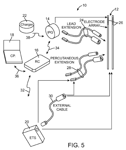
[0049] Turning first to Fig. 5, an exemplary DBS neurostimulation system 10
generally includes one or more (in this case, two) implantable stimulation
leads 12,
an implantable pulse generator (IPG) 14, an external remote controller RC 16,
a
clinician's programmer (CP) 18, an External Trial Stimulator (ETS) 20, and an
external charger 22.
[0050] The IPG 14 is physically connected via one or more percutaneous lead
extensions 24 to the stimulation leads 12, which carry a plurality of
electrodes 26
arranged in an array. In the illustrated embodiment, the stimulation leads 12
are
percutaneous leads, and to this end, the electrodes 26 may be arranged in-line
along
the stimulation leads 12. In alternative embodiments, the electrodes 26 may be
arranged in a two-dimensional pattern on a single paddle lead (e.g., if
cortical brain
stimulation is needed). As will be described in further detail below, the IPG
14
includes pulse generation circuitry that delivers electrical stimulation
energy in the
form of a pulsed electrical waveform (i.e., a temporal series of electrical
pulses) to
the electrode array 26 in accordance with a set of stimulation parameters.
[0051] The ETS 20 may also be physically connected via the percutaneous lead
extensions 28 and external cable 30 to the stimulation leads 12. The ETS 20,
which
has similar pulse generation circuitry as the IPG 14, also delivers electrical
CA 02785799 2012-06-26
WO 2011/082071 PCT/US2010/061839
stimulation energy in the form of a pulse electrical waveform to the electrode
array
26 accordance with a set of stimulation parameters. The major difference
between
the ETS 20 and the IPG 14 is that the ETS 20 is a non-implantable device that
is
used on a trial basis after the stimulation leads 12 have been implanted and
prior to
implantation of the IPG 14, to test the responsiveness of the stimulation that
is to be
provided.
[0052] The RC 16 may be used to telemetrically control the ETS 20 via a bi-
directional RF communications link 32. Once the IPG 14 and stimulation leads
12
are implanted, the RC 16 may be used to telemetrically control the IPG 14 via
a bi-
directional RF communications link 34. Such control allows the IPG 14 to be
turned
on or off and to be programmed with different stimulation parameter sets. The
IPG
14 may also be operated to modify the programmed stimulation parameters to
actively control the characteristics of the electrical stimulation energy
output by the
IPG 14. As will be described in further detail below, the CP 18 provides
clinician
detailed stimulation parameters for programming the IPG 14 and ETS 20 in the
operating room and in follow-up sessions.
[0053] The CP 18 may perform this function by indirectly communicating with
the IPG
14 or ETS 20, through the RC 16, via an IR communications link 36.
Alternatively,
the CP 18 may directly communicate with the IPG 14 or ETS 20 via an RF
communications link (not shown). The clinician detailed stimulation parameters
provided by the CP 18 are also used to program the RC 16, so that the
stimulation
parameters can be subsequently modified by operation of the RC 16 in a stand-
alone mode (i.e., without the assistance of the CP 18).
[0054] The external charger 22 is a portable device used to transcutaneously
charge
the IPG 14 via an inductive link 38. For purposes of brevity, the details of
the
16
CA 02785799 2012-06-26
WO 2011/082071 PCT/US2010/061839
external charger 22 will not be described herein. Once the IPG 14 has been
programmed, and its power source has been charged by the external charger 22
or
otherwise replenished, the IPG 14 may function as programmed without the RC 16
or CP 18 being present.
[0055] For purposes of brevity, the details of the RC 16, CP 18, ETS 20, and
external
charger 22 will not be described herein. Details of exemplary embodiments of
these
devices are disclosed in U.S. Patent No. 6,895,280.
[0056] Referring now to Fig. 6, the features of the stimulation leads 12 and
the IPG
14 will be briefly described. One of the stimulation leads 12(1) has eight
electrodes
26 (labeled E1-E8), and the other stimulation lead 12(2) has eight electrodes
26
(labeled E9-E1 6). The actual number and shape of leads and electrodes will,
of
course, vary according to the intended application. The IPG 14 comprises an
outer
case 40 for housing the electronic and other components (described in further
detail
below), and a connector 42 to which the proximal ends of the stimulation leads
12
mates in a manner that electrically couples the electrodes 26 to the
electronics within
the outer case 40. The outer case 40 is composed of an electrically
conductive,
biocompatible material, such as titanium, and forms a hermetically sealed
compartment wherein the internal electronics are protected from the body
tissue and
fluids. In some cases, the outer case 40 may serve as an electrode.
[0057] The IPG 14 includes a battery and pulse generation circuitry that
delivers the
electrical stimulation energy in the form of a pulsed electrical waveform to
the
electrode array 26 in accordance with a set of stimulation parameters
programmed
into the IPG 14. Such stimulation parameters may comprise electrode
combinations,
which define the electrodes that are activated as anodes (positive), cathodes
(negative), and turned off (zero), percentage of stimulation energy assigned
to each
17
CA 02785799 2012-06-26
WO 2011/082071 PCT/US2010/061839
electrode (fractionalized electrode configurations), and electrical pulse
parameters,
which define the pulse amplitude (measured in milliamps or volts depending on
whether the IPG 14 supplies constant current or constant voltage to the
electrode
array 26), pulse duration (measured in microseconds), pulse rate (measured in
pulses per second), and burst rate (measured as the stimulation on duration X
and
stimulation off duration Y).
[0058] Electrical stimulation will occur between two (or more) activated
electrodes,
one of which may be the IPG case. Simulation energy may be transmitted to the
tissue in a monopolar or multipolar (e.g., bipolar, tripolar, etc.) fashion.
Monopolar
stimulation occurs when a selected one of the lead electrodes 26 is activated
along
with the case of the IPG 14, so that stimulation energy is transmitted between
the
selected electrode 26 and case. Bipolar stimulation occurs when two of the
lead
electrodes 26 are activated as anode and cathode, so that stimulation energy
is
transmitted between the selected electrodes 26. For example, electrode E3 on
the
first lead 12(1) may be activated as an anode at the same time that electrode
El 1 on
the second lead 12(1) is activated as a cathode. Tripolar stimulation occurs
when
three of the lead electrodes 26 are activated, two as anodes and the remaining
one
as a cathode, or two as cathodes and the remaining one as an anode. For
example,
electrodes E4 and E5 on the first lead 12 may be activated as anodes at the
same
time that electrode E12 on the second lead 12 is activated as a cathode.
[0059] The stimulation energy may be delivered between electrodes as
monophasic
electrical energy or multiphasic electrical energy. Monophasic electrical
energy
includes a series of pulses that are either all positive (anodic) or all
negative
(cathodic). Multiphasic electrical energy includes a series of pulses that
alternate
between positive and negative. For example, multiphasic electrical energy may
18
CA 02785799 2012-06-26
WO 2011/082071 PCT/US2010/061839
include a series of biphasic pulses, with each biphasic pulse including a
cathodic
(negative) stimulation pulse and an anodic (positive) recharge pulse that is
generated after the stimulation pulse to prevent direct current charge
transfer
through the tissue, thereby avoiding electrode degradation and cell trauma.
That is,
charge is conveyed through the electrode-tissue interface via current at an
electrode
during a stimulation period (the length of the stimulation pulse), and then
pulled back
off the electrode-tissue interface via an oppositely polarized current at the
same
electrode during a recharge period (the length of the recharge pulse). The
recharge
pulse may be active, in which case, the electrical current is actively
conveyed
through the electrode via current or voltage sources, or the recharge pulse
may be
passive, in which case, the electrical current may be passively conveyed
through the
electrode via redistribution of the charge flowing from coupling capacitances
present
in the circuit.
[0060] As will be discussed in further detail below, the IPG 14 may be
programmed
by the CP 18 (or alternatively the RC 16) to generate four pulsed electrical
waveforms over four respective timing channels to provide treatment to the
patient in
which the IPG 14 is implanted. The electrode combinations assigned to the
respective timing channels will typically be those that result in the
treatment of four
different regions in the patient. Significantly, the IPG 14 allows overlap
between the
electrical pulses generated in the respective timing channels.
[0061] Referring to Fig. 7, one example of using four timing channels to
simultaneously deliver pulsed electrical waveforms to groups of the electrodes
El-
El 6, including the case electrode, will now be described. The horizontal axis
is time,
divided into increments of 1 millisecond (ms), while the vertical axis
represents the
amplitude of a current pulse, if any applied to one of the sixteen electrodes
and case
19
CA 02785799 2012-06-26
WO 2011/082071 PCT/US2010/061839
electrode. Although, for purposes of simplicity, the pulsed electrical
waveforms are
illustrated as being monophasic in nature, it should be appreciated that the
pulsed
electrical waveforms may be multiphasic in nature.
[0062] At time t=0, channel 1 is set to generate and supply a current pulse
having a
pulse amplitude of 4 (milliamps) (mA), a pulse duration of 300 microseconds
(ps),
and a pulse frequency of 200 pulses per second (pps) between electrode El
(which
appears as a 4mA anodic (positive) pulse) and E3 (which appears as a -4mA
cathodic (negative) pulse). At time t=1, channel 2 is set to generate and
supply a
current pulse having a pulse amplitude of 4mA, a pulse duration of 300ps, and
a
pulse frequency of 250pps between electrode El 4 (+4mA) and El 3 (-4mA). At
time
t=2, channel 3 is set to generate and supply a current pulse having a pulse
amplitude
6mA, a pulse duration of 300ps, and a pulse frequency of 200pps between
electrode
E8 (+6mA) and electrodes E6 and E7 (-4mA and -2mA, respectively). At t=3,
channel 4 is set to generate and supply a current pulse having a pulse
amplitude of
5mA, a pulse duration of 400ps, and a pulse frequency of 60pps between
electrodes
El 0 (+5mA) and electrode E8 (-5mA). At t=4, channel 1 is again set to
generate and
supply the current pulse between electrodes El and E3, and channel 2 is again
set
to generate and supply the current pulse between electrodes E14 and E13.
Notably,
although the pulsed electrical waveforms illustrated in Fig. 7 are monophasic
in
nature, the pulsed electrical waveforms delivered during a timing channel can
be
multiphasic in nature.
[0063] As shown in Fig. 8, the stimulation leads 12 are introduced through a
burr
hole 46 formed in the cranium 48 of a patient 44, and introduced into the
parenchyma of the brain 49 of the patient 44 in a conventional manner, such
that the
electrodes 26 are adjacent a target tissue region whose electrical activity is
the
CA 02785799 2012-06-26
WO 2011/082071 PCT/US2010/061839
source of the dysfunction (e.g., the ventrolateral thalamus, internal segment
of
globus pallidus, substantia nigra pars reticulate, subthalamic nucleus, or
external
segment of globus pallidus). Thus, stimulation energy can be conveyed from the
electrodes 26 to the target tissue region to change the status of the
dysfunction.
Due to the lack of space near the location where the stimulation leads 12 exit
the
burr hole 46, the IPG 14 is generally implanted in a surgically-made pocket
either in
the abdomen or above the buttocks. The IPG 14 may, of course, also be
implanted
in other locations of the patient's body. The lead extension(s) 24 facilitates
locating
the IPG 14 away from the exit point of the electrode leads 12.
[0064] Turning next to Fig. 9, the main internal components of the IPG 14 will
now be
described. The IPG 14 includes stimulation output circuitry 50 configured for
generating electrical stimulation energy in accordance with a defined pulsed
waveform having a specified pulse amplitude, pulse rate, pulse width, pulse
shape,
and burst rate under control of control circuitry 51 over data bus 54. The
control
circuitry 51 includes control logic 52, which controls the electrodes to be
activated,
polarity of the active electrodes, and amplitude of the current at the active
electrodes, and timer logic 56, which controls the pulse frequency and pulse
width of
the pulsed electrical waveform. The stimulation energy generated by the
stimulation
output circuitry 50 is output via capacitors C1-C16 to electrical terminals 55
corresponding to the lead electrodes 26, as well as the case electrode 40. As
will be
discussed in further detail below, the stimulation output circuitry 50
comprises anodic
current source circuitry and cathodic current source circuitry, each of which
includes
at least one non-dedicated source (i.e., a source that can be temporally
switched
between selected ones of the lead electrodes 26 and case electrode 40).
21
CA 02785799 2012-06-26
WO 2011/082071 PCT/US2010/061839
[0065] Any of the N electrodes may be assigned to up to k possible groups or
"channels." In one embodiment, k may equal four. The channel identifies which
electrodes are selected to simultaneously source or sink current to create an
electric
field in the tissue to be stimulated. Amplitudes and polarities of electrodes
on a
channel may vary, e.g., as controlled by the CP 18. External programming
software
in the CP 18 is typically used to set stimulation parameters including
electrode
polarity, amplitude, pulse rate and pulse duration for the electrodes of a
given
channel, among other possible programmable features.
[0066] The N programmable electrodes can be programmed to have a positive
(sourcing current), negative (sinking current), or off (no current) polarity
in any of the
k channels. Moreover, each of the N electrodes can operate in a multipolar
(e.g.,
bipolar) mode, e.g., where two or more electrode contacts are grouped to
source/sink current at the same time. Alternatively, each of the N electrodes
can
operate in a monopolar mode where, e.g., the electrode contacts associated
with a
channel are configured as cathodes (negative), and the case electrode (i.e.,
the IPG
case) is configured as an anode (positive).
[0067] Further, the amplitude of the current pulse being sourced or sunk to or
from a
given electrode may be programmed to one of several discrete current levels,
e.g.,
between 0 to 10 mA in steps of 0.1 mA. Also, the pulse duration of the current
pulses is preferably adjustable in convenient increments, e.g., from 0 to 1
milliseconds (ms) in increments of 10 microseconds (ps). Similarly, the pulse
rate is
preferably adjustable within acceptable limits, e.g., from 0 to 1000 pulses
per second
(pps). Other programmable features can include slow start/end ramping, burst
stimulation cycling (on for X time, off for Y time), interphase, and open or
closed loop
sensing modes.
22
CA 02785799 2012-06-26
WO 2011/082071 PCT/US2010/061839
[0068] Significantly, as will be described in further detail below, the
control logic 52
and timer logic 56 control the stimulation output circuitry 50 in such a
manner as to
allow overlap between pulses in the channels despite the fact that a current
source
of the same polarity (either anodic or cathodic) is shared by the electrodes
26.
[0069] The IPG 14 further comprises monitoring circuitry 58 for monitoring the
status
of various nodes or other points 60 throughout the IPG 14, e.g., power supply
voltages, temperature, battery voltage, and the like. The IPG 14 further
comprises
processing circuitry in the form of a microcontroller (pC) 62 that controls
the control
logic over data bus 64, and obtains status data from the monitoring circuitry
58 via
data bus 66. The IPG 14 additionally controls the timer logic 56. The IPG 14
further
comprises memory 68 and oscillator and clock circuitry 70 coupled to the
microcontroller 62. The microcontroller 62, in combination with the memory 68
and
oscillator and clock circuit 70, thus comprise a microprocessor system that
carries
out a program function in accordance with a suitable program stored in the
memory
68. Alternatively, for some applications, the function provided by the
microprocessor
system may be carried out by a suitable state machine.
[0070] Thus, the microcontroller 62 generates the necessary control and status
signals, which allow the microcontroller 62 to control the operation of the
IPG 14 in
accordance with a selected operating program and stimulation parameters. In
controlling the operation of the IPG 14, the microcontroller 62 is able to
individually
generate a train of stimulus pulses at the electrodes 26 using the stimulation
output
circuitry 50, in combination with the control logic 52 and timer logic 56,
thereby
allowing each electrode 26 to be paired or grouped with other electrodes 26,
including the monopolar case electrode. In accordance with stimulation
parameters
stored within the memory 68, the microcontroller 62 may control the polarity,
23
CA 02785799 2012-06-26
WO 2011/082071 PCT/US2010/061839
amplitude, rate, pulse duration and channel through which the current stimulus
pulses are provided. The microcontroller 62 also facilitates the storage of
electrical
parameter data (or other parameter data) measured by the monitoring circuitry
58
within memory 68, and also provides any computational capability needed to
analyze
the raw electrical parameter data obtained from the monitoring circuitry 58
and
compute numerical values from such raw electrical parameter data.
[0071] The IPG 14 further comprises an alternating current (AC) receiving coil
72 for
receiving programming data (e.g., the operating program and/or stimulation
parameters) from the RC 16 (shown in Fig. 5) in an appropriate modulated
carrier
signal, and charging and forward telemetry circuitry 74 for demodulating the
carrier
signal it receives through the AC receiving coil 72 to recover the programming
data,
which programming data is then stored within the memory 68, or within other
memory elements (not shown) distributed throughout the IPG 14.
[0072] The IPG 14 further comprises back telemetry circuitry 76 and an
alternating
current (AC) transmission coil 78 for sending informational data sensed
through the
monitoring circuitry 58 to the CP 18. The back telemetry features of the IPG
14 also
allow its status to be checked. For example, when the CP 18 initiates a
programming session with the IPG 14, the capacity of the battery is
telemetered, so
that the external programmer can calculate the estimated time to recharge. Any
changes made to the current stimulus parameters are confirmed through back
telemetry, thereby assuring that such changes have been correctly received and
implemented within the implant system. Moreover, upon interrogation by the CP
18,
all programmable settings stored within the IPG 14 may be uploaded to the CP
18.
[0073] The IPG 14 further comprises a rechargeable power source 80 and power
circuits 82 for providing the operating power to the IPG 14. The rechargeable
power
24
CA 02785799 2012-06-26
WO 2011/082071 PCT/US2010/061839
source 80 may, e.g., comprise a lithium-ion or lithium-ion polymer battery.
The
rechargeable battery 80 provides an unregulated voltage to the power circuits
82.
The power circuits 82, in turn, generate the various voltages 84, some of
which are
regulated and some of which are not, as needed by the various circuits located
within the IPG 14. The rechargeable power source 80 is recharged using
rectified
AC power (or DC power converted from AC power through other means, e.g.,
efficient AC-to-DC converter circuits, also known as "inverter circuits")
received by
the AC receiving coil 72. To recharge the power source 80, an external charger
(not
shown), which generates the AC magnetic field, is placed against, or otherwise
adjacent, to the patient's skin over the implanted IPG 14. The AC magnetic
field
emitted by the external charger induces AC currents in the AC receiving coil
72. The
charging and forward telemetry circuitry 74 rectifies the AC current to
produce DC
current, which is used to charge the power source 80. While the AC receiving
coil 72
is described as being used for both wirelessly receiving communications (e.g.,
programming and control data) and charging energy from the external device, it
should be appreciated that the AC receiving coil 72 can be arranged as a
dedicated
charging coil, while another coil, such as coil 78, can be used for bi-
directional
telemetry.
[0074] It should be noted that the diagram of Fig. 9 is functional only, and
is not
intended to be limiting. Those of skill in the art, given the descriptions
presented
herein, should be able to readily fashion numerous types of IPG circuits, or
equivalent circuits, that carry out the functions indicated and described,
which
functions include not only producing a stimulus current or voltage on selected
groups
of electrodes, but also the ability to measure electrical parameter data at an
activated or non-activated electrode.
CA 02785799 2012-06-26
WO 2011/082071 PCT/US2010/061839
[0075] Referring now to Fig. 10, the stimulation output circuitry 50 will now
be
described in further detail. The stimulation output circuitry 50 employs
programmable anodic current source circuitry 102, and programmable cathodic
current source circuitry (also known as "current sink circuitry") 104. The
cathodic
source circuitry 104 is similar in design and function the anodic source
circuitry 102,
although differing in polarity. For simplicity and to avoid redundancy, the
components of the anodic current source circuitry 102 and the cathodic current
source circuitry 104 are generically discussed below.
[0076] Each of the anodic and cathodic current source circuitries 102, 104 is
divided
into two parts: a coarse current source portion 106 and a fine current source
portion
108, each of which fractionalizes the current output by the respective current
source
circuitries 102, 104. As its name suggests, the coarse current source portion
106
allows a coarse amount of current to be provided to a particular electrode. In
other
words, the amount of current that can be programmed to be sourced or sunk at a
particular electrode can be adjusted in relatively large increments (e.g.,
5%). By
contrast, the amount of current that can be programmed to be sourced or sunk
at a
particular electrode by the fine current source portion 108 can be adjusted in
relatively small increments (e.g., 1 %).
[0077] Each of the anodic and cathodic current source circuitries 102, 104
also
comprises a master reference digital-to-analog converter (DAC) 110, which
generates a variable reference current lref that is supplied to the coarse
current
source portion 106 and fine current source portion 108 of the respective
current
source. The master DAC 110 of the anodic current source circuitry 102 is
referred to
as a PDAC, and the master DAC 110 of the cathodic current source circuitry 104
is
referred to as an NDAC, reflecting the fact that transistors used in anodic
current
26
CA 02785799 2012-06-26
WO 2011/082071 PCT/US2010/061839
sources are typically formed of P-type transistors that are biased to a high
voltage
(V+), whereas transistors used in cathodic current sources are typically
formed of N-
type transistors that are biased to a low voltage (V-).
[0078] Each master DAC 110 can comprise any structure known in the art for
programming the amplification of current on the basis of a digital control
signal. In
the illustrated embodiment, each master DAC 110 includes eight weighted banks
of
current sources (not shown), and the digital control signal comprises eight
bits that
are respectively inputted along eight lines to the weighted banks of the
master DAC
110, such that the master DAC 110 can be programmed to output 28=256 different
values for the reference current lref. In this way, the currents ultimately
supplied to
the coarse current source portion 106 and fine current source portion 108 can
be
further (and globally) varied by adjusting the gain of the master DAC 110.
[0079] The coarse current source portion 106 does not involve dedicating or
hard-
wiring source circuitry to each electrode. Instead, the coarse current source
portion
106 is shared or distributed amongst the various electrodes via an L number of
coarse current branches 114, each of which includes a current mirror 116 and
an
associated switch bank 118. In the exemplary case, L=1 9. In the illustrated
embodiment, each of the current mirrors 116 outputs the same current
amplitude,
and in particular, a scaled version of the reference current Iref, e.g.,
51ref= In
alternative embodiments, the current output by the current mirrors 116 can be
independently varied.
[0080] Notably, the current mirrors 116 are not individually adjustable in and
of
themselves (in contrast to the master DAC 110). Rather, the current mirrors
116
supply matched currents to the switch banks 118, with selection or not of a
particular
current mirror's 116 current occurring in its given switch bank 118. Each of
the
27
CA 02785799 2012-06-26
WO 2011/082071 PCT/US2010/061839
switch banks 118 contains an N number switches (not shown), which corresponds
to
the number of electrodes. In the exemplary case, N=1 7 (sixteen lead
electrodes 26
and the case electrode). Thus, each switch bank 118 is capable of routing the
current between its current mirror 116 and any of the lead electrodes E1-E16
or case
electrode (not shown in Fig. 10) in response to a digital control signal. In
the case of
the anodic current source circuitry 102, each switch routes the current from
its
current mirror to any of the electrodes, and in the case of the cathodic
current source
circuitry 104, each switch routes the current from any of the electrodes to
its current
mirror.
[0081] In the illustrated embodiment, the digital control signal input into
each switch
bank 118 comprises seventeen bits that are respectively input along seventeen
respective lines to the switches of the switch bank 118, with only one of the
seventeen bits being high, thereby designating the specific switch in the
respective
switch bank 118 to be closed, and thus, the corresponding electrode that
receives
the current from the respective switch bank 118 (in the case of the anodic
current
source circuitry 102) or delivers the current to the respective switch bank
118 (in the
case of the cathodic current source circuitry 104). Thus, only one switch per
coarse
current branch can be closed at one time.
[0082] It can be appreciated from this, that multiple switch banks 118 can
work
together to produce a current at a given electrode. For example, when
operating the
anodic current source circuitry 102, and assuming that each current mirror 116
supplies a current equal to 51ref to its respective switch bank 118, the
coarse current
source portion 106 can supply a maximum current of L*lref = 951ref. If a
current of
501ref was desired at electrode E2, the corresponding switches of any ten of
the
switch banks 118 can be closed, e.g., the first ten switch banks 118(1)-(10)
or the
28
CA 02785799 2012-06-26
WO 2011/082071 PCT/US2010/061839
last ten switch banks 118(10)-(19). Similarly, current can be supplied to
multiple
electrodes at the same time. For example, suppose that 501ref is desired at
electrode
E2; 10lref is desired at electrode E5; and 151ref is desired at electrode E8.
This could
be achieved by closing the switches corresponding to electrode E2 (i.e.,
switches of
ten of the switch banks (e.g., 118(1)-118(10)); closing the switches
corresponding to
electrode E5 of two of the switch banks (e.g., 118(11)-118(12)); and closing
the
switches corresponding to electrode E8 of three of the switch banks (e.g.,
118(13)-
118(15)).
[0083] Because each of the coarse current branches 110 outputs a current equal
to
51ref, the minimum resolution of the coarse current source portion 106 is
51ref.
Accordingly, the fine current source portion 108 additionally provides the
ability to
make fine adjustments to the current at the electrodes. Unlike the coarse
current
source portion 106, the fine current source portion 108 is preferably hard-
wired to
each of the electrodes 26. To the end, the fine current source portion 108
comprises
a fine current DAC 122 hardwired to each of the lead electrodes E1-E16 and
case
electrode (not shown in Fig. 10). The fine current DAC 122 may be similar in
design
and architecture to the master DAC 122 used to set the reference current Iref.
Again,
the fine current DAC 110 of the anodic current source circuitry 102 is
referred to as a
PDAC, and the fine current DAC 110 of the cathodic current source circuitry
104 is
referred to as an NDAC. Each of the fine current DACs 122 receives the
reference
current lref and outputs a variable current in increments of the reference
current lref in
response to a digital input.
[0084] In the exemplary embodiment, each of the DACs 122 has a number J of
fine
current stages that can be activated in response to a digital control signal
to output a
variable current in a defined range, in increments of Iref, to its respective
electrode.
29
CA 02785799 2012-06-26
WO 2011/082071 PCT/US2010/061839
For example, if J=5, each of the DACs 122 may supply a current ranging from
Olref to
51ref to its respective electrode. Thus, the fine current source portion 108
has a
current resolution (Iref) that is smaller than the current resolution (51ref)
of the coarse
current source portion 106. In the illustrated embodiment, the digital control
signal
input into each DAC 122 five bits that are respectively input along five lines
into the
five current stages of the respective DAC 122, such that the DAC 122 can be
programmed to output 6 different scaled values ranging from Olref to 51ref.
[0085] Because of this difference in resolution, both the coarse current
source portion
106 and the fine current source portion 108 can be used simultaneously to set
a
particular current at a given electrode. For example, assuming that it is
desired to
source a current of 531ref to electrode E2, any ten of the coarse current
branches 110
can be activated to deliver 501ref to or from electrode E2. The fine current
DAC 122
coupled to electrode E2 can be programmed to deliver an additional 31ref to or
from
electrode E2, resulting in the desired total current of 531ref at electrode
E2.
[0086] As one skilled in the art will appreciate, it is a matter of design
choice as to
how many coarse current stages L are used, and how many fine current stages J
are
used, and these values may be subject to optimization. However if it is
assumed
that J fine current stages are used, then the number of coarse current stages
L is
preferably equal to (100/J)-1. Thus, if the number of fine current stages J is
equal to
5, the number of coarse current stages L will be equal to 19, thereby allowing
the
coarse current source portion 106 to deliver approximately 95% of the current
range
to or from any electrode with a resolution of approximately 5%, and allowing
the fine
current source portion 108 to deliver approximately 5% of the remaining
current to or
from any electrode at the resolution of approximately 1 %. Although it is
preferred to
use the same reference current Iref as the input to the current mirrors 116 in
the
CA 02785799 2012-06-26
WO 2011/082071 PCT/US2010/061839
coarse current source portion 106 and the DACs 122 in the fine current source
portion 108, different reference currents can be used by the respective coarse
current source portion 106 and fine current source portion 108. In this case,
separate master DAC's may be programmed to generate different reference
currents
that are a scalar of each other.
[0087] In an optional embodiment, the stimulation output circuitry 50 further
comprises a bank of recovery switches (not shown) respectively coupled between
the electrodes and ground. In this case, a digital control signal comprising
seventeen bits can be respectively input to the switches to selectively switch
any of
the electrodes to ground, thereby passively recovering charge at the selected
electrode or electrodes.
[0088] Further disclosure discussing the details of the stimulation output
circuitry 50
can be found in U.S. Patent Publication No. 2007/0100399.
[0089] Referring now to Fig. 11, control circuitry 51 (briefly discussed above
with
respect to Fig. 9) will be described. In response to an input of stimulation
parameter
sets from the microcontroller 62, the control circuitry 51 is configured for
instructing
the stimulation output circuitry 50 to generate and convey a plurality of
pulsed
electrical waveforms between the electrodes in a plurality of timing channels
(e.g., as
shown in Fig. 7 described above), with each pulsed electrical waveform having
a
pulse amplitude, pulse duration, and pulse frequency, as specified by the
respective
stimulation parameter set defined by the microcontroller 62.
[0090] In the illustrated embodiment, up to four pulsed electrical waveforms
can be
respectively generated within four timing channels. However, it should be
appreciated that the number of timing channels may differ. As discussed above,
the
stimulation output circuitry 50 utilizes current source circuitry of different
polarities
31
CA 02785799 2012-06-26
WO 2011/082071 PCT/US2010/061839
(the anodic current source circuitry 102 and the cathodic current source
circuitry 104)
to generate each of the pulsed electrical waveforms. Although the use of both
anodic current source circuitry 102 and cathodic current source circuitry 104
maximizes control of both the anodic and cathodic current amplitudes assigned
to
the respective electrodes, it should be appreciated that only anodic current
source
circuitry or only cathodic current source circuitry may be utilized. It should
also be
appreciated that although the stimulation output circuitry 50 utilizes current
source
circuitry for purposes of current steering, the stimulation output circuitry
50 may
alternatively utilize voltage source circuitry.
[0091] Significantly, irrespective of whether the stimulation output circuitry
50 utilizes
one or both of an anodic electrical source circuitry or cathodic electrical
source
circuitry (whether current or voltage), the control circuitry 51 allows the
pulsed
electrical waveforms to be independently generated within the respective
timing
channels without concern that pulses between the timing channels may overlap,
and
thus, without the need to manipulate the pulsed electrical waveforms in a
manner
that would effectively change the pulse frequencies of the pulsed electrical
waveforms.
[0092] In particular, when the pulses of respective electrical waveforms
generated by
the stimulation output circuitry 50 will not temporally overlap each other,
the control
circuitry 51 instructs the stimulation output circuitry 50 to couple the
anodic source
circuitry 102 to different anodic sets of the electrodes and to couple the
cathodic
source circuitry 104 to different cathodic sets of the electrodes in a
conventional
manner to generate the non-overlapping pulses of the respective pulsed
electrical
waveforms.
32
CA 02785799 2012-06-26
WO 2011/082071 PCT/US2010/061839
[0093] For example, referring back to Fig. 7, timing channel 1 is the only
channel
operating at time t=0, and timing channel 2 is the only channel operating at
time t=1,
and therefore, the control circuitry 51 will instruct the stimulation output
circuitry 50 to
couple the anodic source circuitry 102 to different anodic electrode sets
respectively
during times t=0 and t=1 (i.e., an anodic electrode set comprising electrode
E3 at
t=0, and a different anodic electrode set comprising El 4 at t=1), and to
couple the
cathodic source circuitry 104 to different cathodic electrode sets
respectively during
times t=0 and t=1 (i.e., a cathodic electrode set comprising electrode El at
t=0, and
a different cathodic electrode set comprising El 3 at t=1). In contrast, both
timing
channels 1 and 2 are operated at time t=4, and therefore, the control
circuitry 51 will
instruct the stimulation output circuitry 50 to couple the anodic source
circuitry 102 to
a union of the different anodic electrode sets during time t=4 (i.e., an
anodic
electrode set comprising electrodes E3 and E14), and to couple the cathodic
source
circuitry 104 to a union of the different cathodic electrode sets during time
t=4 (i.e., a
cathodic electrode set comprising electrodes E1 and E13).
[0094] To this end, the control circuitry 51 generally comprises a plurality
of current
steering registers 152 and a plurality of timing registers 154 configured to
be
programmed by the microcontroller 62 in accordance with a respective plurality
of
stimulation parameter sets stored within the microcontroller 62. The control
circuitry
51 further comprises a plurality of timers 156, each of which includes an
input 166
coupled to an output 168 of a respective one of the timing registers 154. The
control
circuitry 51 further comprises a plurality of AND gates 158, each of which
includes a
first input 170 coupled to an output 172 of a respective one of the current
steering
registers 152, and a second input 174 coupled to an output 176 of a respective
one
of the timing timers 154. Because there are four timing channels, and thus,
four
33
CA 02785799 2012-06-26
WO 2011/082071 PCT/US2010/061839
stimulation parameter sets, the control circuitry 51 comprises four
corresponding
current steering registers 152, four corresponding timing registers 154, four
corresponding timers 156, and four corresponding AND gates 158. Notably,
although a single steering register and a single timing register may be used
for each
timing channel, in actuality, each register defined herein may comprise
several
discrete registers. For example, each electrode or a subset of electrodes may
be
associated with its own register. For the purposes of this specification, the
term
"register" may be defined as a set of discrete registers, whether such
register set
includes only one discrete register or a multitude of discrete registers.
[0095] For the corresponding pulsed electrical waveform to be transmitted in
the
corresponding timing channel, each of the current steering registers 152
stores
information related to the electrodes to be activated, as well as the
amplitude and
polarity of the current at the active electrodes, in accordance with the
corresponding
stimulation parameter set stored within the microcontroller 62. For example,
each
current steering register 152 stores a digital representation of the set of
electrodes to
be activated for the respective pulsed electrical waveform to be generated
during the
respective timing channel. In one embodiment, the stored digital
representation of
the active electrode set takes the form of a plurality of binary values
indicative of the
relative current amplitude values to be assigned to the electrodes.
[0096] In the illustrated embodiment, each binary value defines the polarity
and
number of coarse current source branches and fine current source branches of
the
stimulation output circuitry 50 assigned to the respective electrode. In the
exemplary
case, a zero binary value indicates that the corresponding electrode is not to
be
activated, whereas a non-zero binary value indicates that the corresponding
electrode is to be activated at a relative current value defined by the binary
value
34
CA 02785799 2012-06-26
WO 2011/082071 PCT/US2010/061839
(i.e., the number of coarse and fine current branches assigned to the
electrode). In
the illustrated embodiment, a polarity value of "1" indicates that the
electrode is
anodic, whereas a polarity value of "0" indicates that the electrode is
cathodic,
although it should be appreciated that a polarity binary value of "0" may
indicate that
the electrode is anodic, and a polarity value "1" may indicate that the
electrode is
anodic.
[0097] Each current steering register 152 also stores a digital global current
value to
be assigned to the active electrodes for the respective pulsed electrical
waveform to
be generated during the respective timing channel. In the illustrated
embodiment,
the digital global current value is indicative of the reference current lref
output by the
master DAC 110 of the anodic current source circuitry 102 and the cathodic
current
source circuitry 104, which is preferably the same.
[0098] With reference to Figs. 12a-12d, an example of the binary values stored
by
each of the current steering registers 152 will be described.
[0099] As there shown, for Timing Channel 1 (Fig. 12a), a coarse current
binary
value of 00100, a fine current binary value of 100, and a polarity binary
value of 0 are
assigned to electrode El (i.e., four coarse current branches and four fine
current
branches of the cathodic current source circuitry 104 are to be coupled to
electrode
E1), and a coarse current binary value of 00100, a fine current binary value
of 100,
and a polarity binary value of 1 are assigned to electrode El (i.e., four
coarse current
branches and four fine current branches of the anodic current source circuitry
102
are to be coupled to electrode E3).
[00100] For Timing Channel 2 (Fig. 12b), a coarse current binary value of
00100, a
fine current binary value of 100, and a polarity binary value of 0 are
assigned to
electrode E13 (i.e., four coarse current branches and four fine current
branches of
CA 02785799 2012-06-26
WO 2011/082071 PCT/US2010/061839
the cathodic current source circuitry 104 are to be coupled to electrode El
3), and a
coarse current binary value of 00100, a fine current binary value of 100, and
a
polarity binary value of 1 are assigned to electrode E14 (i.e., four coarse
current
branches and four fine current branches of the anodic current source circuitry
102
are to be coupled to electrode E14).
[00101] For Timing Channel 3 (Fig. 12c), a coarse current binary value of
00100, a
fine current binary value of 100, and a polarity binary value of 0 are
assigned to
electrode E6 (i.e., four coarse current branches and four fine current
branches of the
cathodic current source circuitry 104 are to be coupled to electrode E6), a
coarse
current binary value of 00010, a fine current binary value of 010, and a
polarity
binary value of 0 are assigned to electrode E7 (i.e., two coarse current
branches and
two fine current branches of the cathodic current source circuitry 104 are to
be
coupled to electrode E7), and a coarse current binary value of 00111, a fine
current
binary value of 001, and a polarity binary value of 1 are assigned to
electrode E8
(i.e., seven coarse current branches and one fine current branch of the anodic
current source circuitry 102 are to be coupled to electrode E8).
[00102] For Timing Channel 4 (Fig. 12d), a coarse current binary value of
00110, a
fine current binary value of 000, and a polarity binary value of 0 are
assigned to
electrode E8 (i.e., six coarse current branches and zero fine current branches
of the
cathodic current source circuitry 104 are to be coupled to electrode E8), and
a
coarse current binary value of 00110, a fine current binary value of 000, and
a
polarity binary value of 1 are assigned to electrode E10 (i.e., six coarse
current
branches and zero fine current branches of the anodic current source circuitry
102
are to be coupled to electrode El 0).
36
CA 02785799 2012-06-26
WO 2011/082071 PCT/US2010/061839
[00103] As can be seen in Figs. 12a-12d, a coarse current binary value of
00000 and
a fine current binary value of 000 are assigned to all inactive electrodes.
For all of
the timing channels, the digital global current value is set to be 10000000,
such that
half of the total anodic current and cathodic current is made available to the
active
electrodes by the master DAC's 110. Thus, the assignment of coarse current
branches and fine current branches defines the relative current amplitudes at
the
active electrodes, while the setting of the master DAC's 110 ultimately
defines the
global current amplitude at the active electrodes.
[00104] For the corresponding pulsed electrical waveform to be transmitted in
the
corresponding timing channel, each of the timing registers 154 stores
information
related to the pulse frequency and pulse duration in accordance with the
corresponding stimulation parameter set stored within the microcontroller 62.
[00105] Referring back to Fig. 11, each of the timers 156 outputs a phase
enabling
178 signal in accordance with a pulse duration and pulse frequency defined by
the
timing information stored in the respective timing registers 154. That is, the
phase
enabling signal 178 output by each timer 154 will be high (i.e., logical "1 ")
for a time
equal to the duration of the pulses to be generated and at a frequency equal
to the
frequency of the pulses to be generated. Thus, it can be appreciated that,
when the
phase enabling signal 178 is high (i.e., logical "'I"), the digital contents
stored in the
corresponding register 152 are gated to an output 180 of the AND gate 158 for
a
period of time equal to the pulse duration and at a frequency equal to the
pulse
frequency defined in the corresponding timing register 154.
[00106] The control circuitry 51 further comprises an OR gate 160 having
inputs 182-
188 coupled to the output 180 of each of the respective AND gates 158. Thus,
any
digital contents of the respective registers 152 (including the digital
representations
37
CA 02785799 2012-06-26
WO 2011/082071 PCT/US2010/061839
of the active electrode sets) that are gated to the respective outputs 180 of
the AND
gates 156 are combined at an output 190 of the OR gate 160 in a bit-wise
manner
(e.g., the first bit of a first set of gated digital contents is AND'd with
the first bit of a
second set of gated digital contents; the second bit of the first set of gated
digital
contents is AND'd with the second bit of the second set of gated digital
contents,
etc.) to create a union of the digital contents (effectively creating a union
of the active
electrodes sets in the respective timing channels). Notably, when the digital
contents of only one of the registers 152 are currently gated to its
respective AND
gate 158 (i.e., no pulses will overlap), the union of the digital contents at
the output
190 of the OR gate 160 will simply be the gated digital contents of that one
current
steering register 152. In contrast, when the digital contents of more than one
of the
current steering registers 152 are currently gated to their respective AND
gates 156
(i.e., the pulses overlap), the union of the digital contents at the output
190 of the OR
gate 160 will be the union of the multiple gated digital contents.
[00107] For example, referring back to Fig. 7, during time t=0, the union of
the gated
digital contents at the output 190 of the OR gate 160 will simply be the
digital
contents gated from the first register 152 (corresponding to timing channel
1); that is,
the coarse current branch values, fine current values, and polarity values
associated
with electrodes El and E3, and during time t=1, the union of the gated digital
contents at the output 190 of the OR gate 160 will simply be the digital
contents
gated from the second register 152 (corresponding to timing channel 2); that
is, the
coarse current branch values, fine current values, and polarity values
associated
with electrodes E13 and E14. In contrast, during time t=4, the union of the
gated
digital contents at the output 190 of the OR gate 160 will be the union of the
digital
contents gated both from the first register 152 and the second register 152,
as
38
CA 02785799 2012-06-26
WO 2011/082071 PCT/US2010/061839
illustrated in Fig. 13. Notably, because the global current values will
presumably be
the same for all of the timing channels, the union of the global current
values will be
identical to the global current value.
[00108] It should be noted that although only one AND gate 158 per timing
channel is
illustrated, there may be multiple AND gates per timing channel. For example,
certain portions of the digital contents within the current steering timing
registers may
be respectively gated to the outputs of the multiple AND gates 158 by the
phase
enabling signals 178. For example, for each timing channel, the global
amplitude
binary values may be gated to the output of a AND gate, the coarse branch
binary
values and polarity value may be gated to the output of another AND gate, and
the
fine branch binary values may be gated to the output of still another AND
gate.
[00109] By the same token, it should also be noted that although only one OR
gate
160 is illustrated for all timing channels, there may be multiple OR gates for
all timing
channels. For example, an OR gate can be provided for each portion of the
digital
contents within the current steering timing registers to be combined. For
example,
the global amplitude binary values gated to the respective outputs of AND
gates can
be combined at the output of an OR gate to create a union of the global
amplitude
binary values, the coarse branch binary values and polarity value gated to the
respective outputs of AND gates can be combined at the output of another OR
gate
to create a union of the coarse branch binary values and polarity values, and
the fine
branch binary values gated to the respective outputs of AND gates can be
combined
at the output of still another OR gate to create a union of the fine branch
binary
values.
39
CA 02785799 2012-06-26
WO 2011/082071 PCT/US2010/061839
[00110] In any event, the OR gate 160 outputs the union of the global current
values,
the union of the coarse branch binary values, and the union of the fine branch
binary
values.
[00111] The union of the global current values gated at the output 190 of the
OR gate
160 is routed as a digital control signal, which includes 8 bits, along eight
lines
directly to each of the master DACs 110 (see Fig. 10). For example, with
reference
to Fig. 13, the binary control signal 10000000 will be routed to each of the
master
DACs 110 to deliver half of available current to or from the anodic and
cathodic
current source circuitries 102, 104.
[00112] The control circuitry 51 further comprises a coarse branch decoder and
distribution circuit 162 that obtains the union of the coarse current branch
values and
polarity values gated at the output of the OR gate 160, and sends a digital
control
signal to the corresponding anodic and cathodic switch banks 118 . In the
illustrated
embodiment, the coarse branch decoder and distribution circuit 162 receives
102
bits (17 electrodes x 6 bits (five coarse branch bits and one polarity bit))
from the
output 190 of the OR gate 160, and outputs nineteen digital control signals,
each of
which comprises 17 bits, along 17 lines to the respective anodic switch banks
118
(see Fig. 10), and nineteen digital control signals, each of which comprises
17 bits,
along 17 lines to the respective cathodic switch banks 118 (see Fig. 10).
[00113] For example, with reference to Fig. 13, the coarse branch decoder and
distribution circuit 162 will , in accordance with the coarse current branch
binary
value "00100" and polarity value "0" associated with electrode El, make line 1
high
and the remaining lines low for four switch banks 118 of the cathodic current
source
circuitry 104 to deliver current from the electrode El to four of the coarse
current
branches 114 (20% of the cathodic current); in accordance with the coarse
current
CA 02785799 2012-06-26
WO 2011/082071 PCT/US2010/061839
branch binary value "00100" and polarity value "1" associated with electrode
E3,
make line 3 high and the remaining lines low for four switch banks 118 of the
anodic
current source circuitry 102 to deliver current from four of the coarse
current
branches 114 to electrode E3 (20% of the anodic current); in accordance with
the
coarse current branch binary value "00100" and polarity value "0" associated
with
electrode El 3, make line 13 high and the remaining lines low for four switch
banks
118 of the anodic current source circuitry 102 to deliver current from four of
the
coarse current branches 114 to electrode E13 (20% of the anodic current); in
accordance with the coarse current branch binary value "00100" and polarity
value
"1" associated with electrode E14, make line 14 high and the remaining lines
low for
four switch banks 118 of the cathodic current source circuitry 104 to deliver
current
from electrode E14 to four of the coarse current branches 114 (20% of the
cathodic
current).
[00114] The control circuitry 51 further comprises a fine branch decoder
circuit 164
that obtains the union of the fine current branch values and polarity values
gated at
the output of the OR gate 160, and sends a digital control signal to the
corresponding anodic and cathodic fine branch DACs 122 . In the illustrated
embodiment, the fine branch decoder circuit 164 receives 68 bits (17
electrodes x 4
bits (three fine branch bits and one polarity bit)) from the output 190 of the
OR gate
160, and outputs seventeen digital control signals, each of which comprises 5
bits, to
the fine PDACs 122 (see Fig. 10), and seventeen digital control signals, each
of
which comprises 5 bits, to the fine NDACs 122 (see Fig. 10).
[00115] For example, with reference to Fig. 13, the fine branch decoder
circuit 164
will, in accordance with the fine current branch binary value "100" and
polarity value
"0" associated with electrode El, make lines 1-4 high and line 5 low for the
fine
41
CA 02785799 2012-06-26
WO 2011/082071 PCT/US2010/061839
NDAC 122 associated with electrode El to deliver current from electrode El to
four
of the fine current branches (4% of the cathodic current); in accordance with
the fine
current branch binary value "100" and polarity value "1 " associated with
electrode
E3, make lines 1-4 high and line 5 low for the fine PDAC 122 associated with
electrode E3 to deliver current from four of the fine current branches to
electrode E3
(4% of the cathodic current); in accordance with the fine current branch
binary value
"100" and polarity value "0" associated with electrode E13, make lines 1-4
high and
line 5 low for the fine NDAC 122 associated with electrode E13 to deliver
current
from four of the fine current branches to electrode El 3 (4% of the cathodic
current);
and in accordance with the fine current branch binary value "100" and polarity
value
"1" associated with electrode E14, make lines 1-4 high and line 5 low for the
fine
PDAC 122associated with electrode El 4 to deliver current from electrode El 4
to four
of the fine current branches (4% of the cathodic current).
[00116] Notably, for each current source at any given time, each of the timing
channels can use any number of the coarse current branches as long as the
total
number does not exceed L (i.e., the total number of coarse current branches
for
each current source). Thus, as long as number of coarse current branches
required
by the timing channels at any given time does not exceed the total number of
coarse
current branches available, one timing channel will not affect another timing
channel.
Thus, because the timing channels can be operated to simultaneously deliver
pulses, the pulsed electrical waveforms can have independent frequencies.
[00117] It should also be noted that, when passive recharge pulses are
utilized, the
use of the currently activated electrodes in any particular timing channel can
be
stored in a charge recovery module (not shown) associated with the respective
timing channel. The timer associated with the timing channel can enable
passive
42
CA 02785799 2012-06-26
WO 2011/082071 PCT/US2010/061839
recovery in the activated electrodes by enabling passive recovery switches
(not
shown) coupled between these electrodes and ground. During passive recovery,
passive recovery signals for the electrodes can be gated on through an AND
gate
(not shown) by the timer and the output combined with the passive recovery
signals
of other timing channels through an OR gate (not shown). The passive recovery
signals at the output of the OR gate can then be sent to the recovery
switches.
When an active pulse coincides with a charge recovery pulse, the passive
recovery
signals may be automatically inhibited (gated off) until the end of the active
pulse. At
the end of the active pulse, recovery resumes until the end of the passive
recovery
phase.
[00118] Although particular embodiments of the present inventions have been
shown
and described, it will be understood that it is not intended to limit the
present
inventions to the preferred embodiments, and it will be obvious to those
skilled in the
art that various changes and modifications may be made without departing from
the
spirit and scope of the present inventions. Thus, the present inventions are
intended
to cover alternatives, modifications, and equivalents, which may be included
within
the spirit and scope of the present inventions as defined by the claims.
43