Note: Descriptions are shown in the official language in which they were submitted.
CA 02808490 2014-09-18
1
Power Conversion with Added Pseudo-Phase
BACKGROUND
[0001] The present application relates to power conversion
methods, systems, and devices, and more particularly to nonresonant
conversion architectures.
[0002] Note that the points discussed below may reflect the
hindsight gained from the disclosed inventions, and are not necessarily
admitted to be prior art.
[0003] Power conversion is one of the most important
applications of power semiconductors, and plays an important role in many
systems. Power conversion can be used to shift the voltage of a power
supply to match the operating requirements of a particular load, or to permit
use of a variable-voltage or variable current supply, or to compensate for the
variation expected in an unreliable power source, or to permit a unit to be
usable with a variety of power inputs, or to compensate for shift in "power
factor" when an AC supply is connected to a reactive load. In many cases
there are different terms for particular kinds of power conversion, e.g. a DC-
to-AC converter is often referred to as an inverter, and some types of AC-to-
AC converter are referred to as cydoconverters. Many kinds of motor drive
can be thought of as a kind of power conversion: for example, a variable-
frequency drive can be regarded as a species of power converter in which the
frequency of an AC output is adjustable. In the present application the term
"power conversion" will be used to refer generically to all of these types.
CA 02808490 2014-09-18
2
[0004] The present inventor has previously filed on a new class
of power converter device operation and device, which provides a nearly
universal power conversion architecture. In one version of this architecture,
each input line is connected to the middle of one phase leg having two
bidirectional switches, and the switches are operated so as to drive the
terminals of a link reactance from one input or the other. A corresponding
output switch array is used to transfer energy from the link reactance into
two or more output terminals as desired, to construct the output waveform
desired. Preferably the link reactance includes an inductor which is shunted
by a capacitor. This provides a nearly universal hardware architecture,
which is operated to implement a desired power-conversion function. This
architecture is suitable for DC-AC, AC-AC, and AC-DC conversion.
However, the present inventor now provides additional improvements,
which are applicable to these as well as other topologies.
[0005] Many DC-DC, DC-AC, and AC-AC Buck-Boost
converters are shown in the patent and academic literature. The classic
Buck-Boost converter operates the inductor with continuous current, and the
inductor may have an input and output winding to form a transfer for
isolation and/or voltage/current translation, in which case it is referred to
as
a Flyback Converter. There are many examples of this basic converter, all of
which are necessarily hard switched and therefore do not have the soft-
switched attribute, which leads to reduced converter efficiency and higher
costs.
[0006] In a chain of patent applications dating back to 2006, the
present inventor has disclosed a revolutionary new power conversion
architecture, known as the "UPC" (or "Universal Power Conversion")
CA 02808490 2014-09-18
3
architecture. The present application describes further improvements which
are particularly advantageous in connection with UPC architectures, and
may also be applicable to other architectures.
SUMMARY
[0007] The present application discloses new approaches to
power conversion and related applications. An energy storage leg, including
a capacitor plus switching which connects the capacitor reversibly across a
primary link reactance, is added to at least one port of a power converter.
Preferably the power converter has an architecture, such as that of the
"Universal Power Converter," which would be functional even without the
energy storage leg.
[0008] The disclosed innovations, in various embodiments,
provide one or more of at least the following advantages. However, not all
of these advantages result from every one of the innovations disclosed, and
this list of advantages does not limit the various claimed inventions.
= Increased ability to harvest available energy from "green" sources,
including wind and solar power;
= Increased lifetime for microinverters;
= Compact size for variable frequency drive units;
= Increased availability of variable frequency drive in residential
applications;
= Increased ability to generate pulsed waveforms from DC or low-
frequency power inputs.
CA 02808490 2014-09-18
4
BRIEF DESCRIPTION OF THE DRAWINGS
[0009] The disclosed inventions will be described with reference
to the accompanying drawings, which show important sample embodiments
of the invention:
[00010] Figure 1A schematically shows a modified Universal
Power Converter circuit configuration, which includes an energy storage
capacitor with a bridge circuit to provide a "pseudo-phase".
[00011] Figure 1B schematically shows another modified
Universal Power Converter circuit configuration, which includes an energy
storage capacitor with a full-bridge configuration.
[00012] Figure 1C schematically shows yet another modified
Universal Power Converter circuit configuration.
[00013] Figure 1D schematically shows a system in which a
pseudo-phase power converter provides a Variable Frequency Drive output
to an appliance (in this example the compressor motor of an air conditioner),
in an environment where three-phase power is not available.
[00014] Figure 1E schematically shows a system in which a
pseudo-phase power converter converts power from a wind-driven alternator
to provide residential (or other) power supply at standard voltage and
frequency.
[00015] Figure 1F schematically shows a solar energy system in
which a pseudo-phase power converter provides a microinverter which
efficiently converts the photovoltaic power to provide residential (or other)
power supply at standard voltage and frequency.
[00016] Figure 1G shows a sample embodiment in a Full-Bridge
Buck-Boost Converter.
CA 02808490 2014-09-18
[00017] Figures 2a-2d show four alternative versions of the basic
Bi-directional Conducting and Blocking Switch (BCBS) used in the circuit
of Figure 1.
[00018] Figure 3 shows a conventional "Standard Drive".
[00019] Figure 4 shows a conventional hard-switched three phase
to three phase AC buck-boost converter.
[00020] Figure 5 shows a conventional soft-switched "partial
resonant" three phase to three phase AC buck-boost converter, and Figure 6
shows the inductor current and voltage waveforms for the converter of
Figure 5.
[00021] Figures 7 and 8 show other conventional converters.
[00022] Figure 9 shows the input line voltages, and Figure 10
shows the output line voltages, for the current switching example of Figures
11, 12a-12j, and 13.
[00023] Figure 11 summarizes the line and inductor current
waveforms for several inductor cycles.
[00024] Figures 12a-12j show voltage and current waveforms on
the inductor during a typical cycle.
[00025] Figure 13 shows voltage and current waveforms
corresponding to the full power condition of Figure 12, and Figure 14 shows
inductor voltage and current for an output voltage of about half the full
output voltage.
[00026] Figure 15 shows another embodiment, which includes
Controls and I/O Filtering.
CA 02808490 2014-09-18
6
[00027] Figure 16 illustrates current and timing relationships in
yet other embodiments, and Figure 17 shows these relationships when the
output voltage is half of the input voltage.
[00028] Figure 18 is a spreadsheet which calculates the average
output current for a given set of conditions, as the current discharge time is
varied, and Figure 19 shows the results of this calculation under various
conditions.
[00029] Figure 20 is a version of Figures 16 and 17 which shows
inductor current and timing for a regeneration condition where the output
voltage is 1/2 of the input.
[00030] Figure 21 shows yet another embodiment, with DC or
single Phase portals.
[00031] Figure 22 shows yet another embodiment, with a
transformer.
[00032] Figure 23 shows yet another embodiment, in a four
portal configuration.
[00033] Figure 24 shows yet another embodiment, in a three
portal application mixing three phase AC portals and a DC portal, as may be
used to advantage in a Hybrid Electric Vehicle application.
[00034] Figures 25 and 26 show two more classes of
implementations using half-bridge topologies.
[00035] Figure 27 shows yet another embodiment, which
provides a single phase to three phase synchronous motor drive.
[00036] Figure 28 shows yet another embodiment, with dual
power modules.
CA 02808490 2014-09-18
7
[00037] Figure 29 shows yet another embodiment, which
provides a three phase Power Line Conditioner.
DETAILED DESCRIPTION OF SAMPLE EMBODIMENTS
[00038] The numerous innovative teachings of the present
application will be described with particular reference to presently preferred
embodiments (by way of example, and not of limitation). The present
application describes several inventions, and none of the statements below
should be taken as limiting the claims generally.
[00039] This application describes implementations and/or
improvements on the concepts described in US Application no. 11/759006
filed 6/6/2007 and now published as US2008/0013351, and in US
Application no. 11/7580970, now published as US2008/0031019. These
applications describe many key concepts, and many other implementations,
of the Universal Power Converter. Each of these applications has
copendency, common inventorship, and common ownership with the present
application.
[00040] Figure 1A shows a first example 100A of the innovative
pseudo-phase UPC circuit topology. The two lines of a single-phase input
are connected into respective phase legs PL2 and PL2, both of which are
connected to a common pair of lines 113/114.
[00041] Note that an energy storage section 101 has been added
to the UPC in order to buffer energy transfers involving a single phase AC
power source or sink. In this example, the energy storage section 101
includes four AC (bi-directional) switches which allow power transfer to or
from a connected energy storage capacitor ESC. This power transfer may
CA 02808490 2014-09-18
8
occur in either direction between the capacitor ESC and the link inductor LI,
or in either direction between the capacitor ESC and an external port.
[00042] The link inductor LI (with its shunt capacitor Cs) is
directly connected to the lines 113/114, but all other components are
connected only through switches. Thus the link inductor can be completely
isolated by disconnected all the other components from the common lines
113/114.
[00043] Passive components are used for filtering on the input
and output connections, but other configurations besides that shown can be
used.
[00044] The common lines 113/114 connect the link inductor LI
to the input port and to the energy storage section 101, but also to an output
port. In this example three phase legs PA, PB, and Pc are used to drive three
output lines as described below.
[00045] Thus, when the single phase AC input (on the two
terminals at the left side of this drawing) is at or near maximum voltage,
power is transferred on each cycle of the link inductor (or link reactance)
LI,
from the AC input to both the three phase output and the energy storage
capacitor. When the single phase AC input is at or near zero voltage, all
output power comes from the energy storage capacitor ESC. At some
intermediate AC input voltage, power transfer is only between the input and
the three phase output.
[00046] The disclosed inventions take advantage of the multi-port
capability of the UPC to avoid the use of electrolytic capacitors in single
phase power converters, and also allows a single UPC to accomplish low
harmonic single phase to three phase operations.
CA 02808490 2014-09-18
9
[00047] The disclosed inventions may also be used to accomplish
DC to single phase conversion, single phase to DC conversion, or single
phase to single phase conversion with or without frequency conversion, all
without the use of electrolytic capacitors.
[00048] To minimize the size of the film capacitor used for the
energy storage capacitor, the voltage on the energy storage capacitor is made
to vary over an almost 2 to 1 voltage range, taking advantage of the buck-
boost capability of the UPC.
Single Phase to Multi-Phase
[00049] Single phase to three phase conversion is of particular
value in residential variable speed AC applications, in which the single
phase input is transferred, with unity power factor and low harmonics, to a
variable voltage and frequency output to drive an induction motor at variable
speeds, as may be used to minimize the power consumption of an AC unit.
[00050] Charging: When the Single Phase line is at maximum
voltage, we can charge the energy storage capacitor (ESC) while providing
full three phase power to the motor, as follows:
[00051] 1. The link inductor LI (LI) charges to full current from
the single phase input line (at max voltage).
[00052] 2. The link inductor LI disconnects from the input and
undergoes voltage reversal.
[00053] 3. The link inductor LI discharges some energy into the
lowest voltage phase pair of the motor (and therefore the current on the Link
Inductor LI drops).
CA 02808490 2014-09-18
[00054] 4. The link inductor LI disconnects from that lowest
voltage phase pair, and then (as an isolated inductor with stored energy) its
voltage ramps up.
[00055] 5. When the Link Inductor's voltage exceeds that of the
highest voltage phase pair of the motor, the the link inductor LI LI is
connected to discharge more energy into the highest voltage phase pair.
[00056] 6. The link inductor LI is then disconnected from the
highest voltage phase pair, and then (as an isolated inductor with stored
energy) its voltage ramps up again.
[00057] 7. When the voltage on the link inductor LI ramps up to
the voltage on the energy storage capacitor ESC, the link inductor LI is
connected to discharge its remaining energy into the energy storage
capacitor ESC.
[00058] 8. The above cycle 1-7 is repeated, but with reversed
current on the link inductor LI.
[00059] Discharging: When the Single Phase line is at zero or
low voltage, we discharge the energy storage capacitor (ESC) while
providing full three phase power to motor, as follows:
[00060] 1. The link inductor LI charges to a suitable current from
the energy storage capacitor ESC.
[00061] 2. The link inductor LI is disconnected from The Energy
Storage Capacitor, and its voltage ramps down to that of the single phase
line.
[00062] 3. The link inductor LI is then connected to be chargee to
higher current from the single phase line input.
CA 02808490 2014-09-18
11
[00063] 4. The link inductor LI is then disconnected from the
input, and undergoes voltage reversal.
[00064] 5. The link inductor LI discharges some energy into
lowest voltage phase pair of the output motor, and hence the current on link
inductor LI drops.
[00065] 6. The link inductor LI is then disconnected from the
lowest voltage phase pair, and its voltage then ramps up to highest voltage
phase pair of motor.
[00066] 7. The link inductor LI is then connected to discharge its
remaining energy into the highest voltage phase pair.
[00067] 8. The above cycle 1-7 is repeated, but with reversed
current through the link inductor LI.
[00068] This use of the energy storage section shows why the
converters using it are referred to as "pseudo-phase" converters. In general,
the energy storage section provides energy storage with a flexibility of
timing which provides great synergistic advantages in combination with the
Universal Power Converter topology.
[00069] Figure 1D shows an example of a system incorporating
conversion of this type. In this sample embodiment, a residential air
conditioning unit is driven with variable frequency, by use of a pseudo-
phase converter to generate a variable-frequency three-phase output. In the
example show, the compressor motor M1 is driven with three-phase, and the
blower motor M2 is driven with the normal 120/240V single phase (or split-
phase line); alternatively, two modules 100 can be used to provide
independently controlled variable-speed outputs.
CA 02808490 2014-09-18
12
[00070] Figure 1B schematically
shows another modified
Universal Power Converter circuit configuration, which includes an energy
storage capacitor with a full-bridge configuration.
Multiphase to Single-Phase
[00071] Figure 1B schematically
shows another modified
Universal Power Converter circuit configuration 100B, which includes an
energy storage capacitor with a full-bridge configuration. Note that the
energy storage section 101 is located on the output side here, which is where
the single-phase port is.
[00072] Figure 1E shows an
example of a system configuration
in which this configuration can be particularly useful. With wind-powered
electricity generation the available power is inherently variable, and
(depending on the electrical configuration used) may result in an AC power
output which has variable frequency and/or variable voltage. In the
example shown in this Figure, the power from the wind power source is
three-phase, with an unpredictable frequency which is typically in the range
of 20-80Hz (depending on conditions). The pseudo-phase converter 100 is
used to translate this power into standard voltage and frequency, and (if
desired) to lock the phase precisely to the local power grid.
DC to AC
[00073] Another possibly
significant application of this invention
is for Solar PV micro-inverters, which convert the steady DC power of a PV
array into the pulsating power of residential single phase AC. All other
micro-inverters require using electrolytic capacitors, which have a limited
life span.
CA 02808490 2014-09-18
13
[00074] Figure IC schematically shows yet another modified
Universal Power Converter circuit configuration 100C. In this example a
DC input is connected to two input phase legs PL1 and PL2, which drive the
link inductance as described above. Here, however, the link inductance LI'
is a transformer. Operation is generally as described above, except that the
transformer provides some voltage translation and phase shift between the
common rails on the left side and those on the right side. Here the energy
storage unit 101 is on the output side, and provides better efficiency by
buffering input power when the AC output is near a zero-crossing. The
efficient use of the capacitor ESC helps to provide efficient and compact
realizations.
[00075] The configuration of Figure 1C provides a
microconverter, which is useful for solar power systems as described below.
In a sample embodiment, for a microinverter rated at 200 watts for
conversion of 40 VDC to 125 VAC single phase, the ESC is about 40 F,
and is operated (on the high voltage side of the circuit) at a voltage which
varies cyclically from about 100 to 200 VDC, cycling at 120 Hz.
[00076] Figure IF provides an example of a solar energy system
using a pseudo-phase power converter 100, which can optionally be the
same as converter 100C of Figure 1C. Here a photovoltaic stack provides a
DC voltage to the converter 100, which converts the DC input into a single-
phase AC output. Optionally a grid connection is provided, so that power
can be fed back into the mains, or at least kept in phase with mains power.
[00077] Many features and modifications of the basic UPC
architecture will now be described, to help show other advantages and
modifications of the pseudo-phase versions of the UPC.
CA 02808490 2014-09-18
14
[00078] The present application discloses power converters which
are generally of the Buck-Boost family, but which use capacitance, either
parasitic alone or with added discrete device(s), in parallel with the Buck-
Boost inductor to achieve low turn-off switching stresses (i.e. "soft
switching") on the semiconductor switches, allowing relatively slow and
inexpensive switches to be used. In alternative disclosed embodiments, as
discussed below, operation without such added capacitance is possible, at
the expense of higher forward turn-off switching losses.
[00079] In Figure 1G, and various other disclosed embodiments,
even if little or no parallel capacitance is used, switch turn on always
occurs
as the switch transitions from reverse to forward bias, allowing for low turn-
on losses. Reverse recovery of the switches is accomplished with low rates
of current decrease, and with low reverse recovery voltage, leading to near
zero loss reverse recovery switching.
[00080] The embodiments described below are improvements on
the "Full Cycle" mode of the parent applications, which results in two power
transfers per inductor cycle. Buck-Boost converters, including those of the
Ngo and Kim references cited above, have a DC bias in the inductor current,
and only one power transfer per inductor cycle.
[00081] The disclosed inventions can also be used for DC-AC,
AC-DC, AC-AC, or DC-DC conversion, with no limitation on the relative
magnitudes of the voltages involved as long as the voltage rating of the
switches is not exceeded. However, if the implementation is such that one
portal is always a higher voltage than the other portal, then the switches
connected to said higher portal need only be able to block voltage in one
direction.
CA 02808490 2014-09-18
[00082] Full electrical isolation and/or greater voltage and current
conversion may be achieved by using an inductor/transformer instead of the
simple inductor. Note that the inductor/transformer will typically not have
current in both sides at the same time, so its operation is more like a split
inductor (as in a flyback converter) than like a simple transformer (as in a
push-pull converter. Another significant different between buck-boost and
push-pull is that the push-pull output voltage is fixed as a multiple or
fraction of the input voltage, as given by the turns ratio, while the buck-
boost has no such limitation. Push-pull topologies are described at
http://en.wikipedia.org/wild/Push-Pull_Converter (in its state as of the
filling
date). A push-pull is quite unlike a buck-boost or flyback converter, in that
the transformer is not operated as an energy-transfer inductor. In a buck-
boost or flyback, input current pumps energy into a magnetic field, which is
then drained to drive output current; thus the input and output currents flow
at different times.
[00083] Inductor/transformer leakage inductance is typically a
significant concern of buck-boost designs. This is typically dealt with by
minimizing the leakage, and sometimes by adding circuit elements to deal
with it. By contrast, many of the embodiments described below can tolerate
large parasitic capacitance, and thus inductors or transformers with very
close windings can be specified, to minimize the leakage inductance. The
standard hard switched buck-boost cannot tolerate parasitic capacitance,
which makes it very difficult to minimize the leakage inductance for those
configurations.
[00084] The innovative converter circuits, in various elements are
constructed of semiconductor switches, an inductor, advantageously a
CA 02808490 2014-09-18
16
capacitor in parallel with the inductor, and input and output filter
capacitances. A control means, controlling the input switches, first connects
the inductor, initially at zero current, to the input voltage, which may be DC
or the highest line-to-line voltage AC pair in a three phase input, except at
startup, in which case a near zero-voltage line pair is used. The control then
turns off those switches when the current reaches a point determined by the
control to result in the desired rate of power transfer. The current then
circulates between the inductor and capacitor, which results in a relatively
low rate of voltage increase, such that the switches are substantially off
before the voltage across them has risen significantly, resulting in low turn-
off losses.
[00085] With DC or single phase
AC input, no further current is
drawn from the input. With three phase AC input, the control will again
connect the inductor to the input lines, but this time to the line-to-line
pair
which has a lower voltage then the first pair. Turn on is accomplished as the
relevant switches transition from reverse to forward bias. After drawings the
appropriate amount of charge (which may be zero if the control determines
that no current is to be drawn from the pair, as for example that the pair is
at
zero volts and input unity power factor is desired), the relevant switches are
again turned off. Under most conditions, the voltage on the inductor will
then reverse (with relatively low rates of voltage change due to the parallel
capacitance). With three phase AC output, the control will turn on switches
to allow current to flow from the inductor to the lowest voltage pair of lines
which need current, after the relevant switches become forward biased, with
the control turning off the switches after the appropriate amount of charge
has been transferred. The inductor voltage then ramps up to the highest
CA 02808490 2014-09-18
17
output line-to-line pair for three phase AC, or to the output voltage for
single
phase AC or DC. Again, switches are turned on to transfer energy (charge)
to the output, transitioning from reverse to forward bias as the voltage ramps
up. If the output voltage is larger then the highest input voltage, the
current
is allowed to drop to zero, which turns off the switch with a low rate of
current reduction, which allows for the use of relatively slow reverse
recovery characteristics. If the output voltage is less then the highest input
voltage, the switches are turned off before current stops, so that the
inductor
voltage ramps up to the input voltage, such that zero-voltage turn on is
maintained. Alternatively, the switches may be turned off before the point
cited in the previous sentence, so as to limit the amount of current into the
output. In this case, the excess energy due to current in the inductor is
directed back into the input by turning on switches to direct current flow
from the inductor into either the highest voltage pair in three phase, or the
single phase AC or DC input.
[00086] In a three phase AC
converter, the relative charge per
cycle allocated to each input and output line pair is controlled to match the
relative current levels on each line (phase). After the above scenario, when
zero current is reached the inductor is reconnected to the input, but with a
polarity reversed from the first connection, using switches that are
complimentary to the switches used in the first half of the cycle. This
connection can occur immediately after zero current (or shortly after zero
current if the input voltage is less than the output voltage, to allow the
capacitor voltage time to ramp back down), giving full utilization of the
power transfer capability of the inductor. No resonant reversal is required as
in the time period M4 of the Kim converter shown in Figures 5 and 6.
CA 02808490 2014-09-18
18
[00087] The disclosed embodiments are inherently capable of
regeneration at any condition of output voltage, power factor, or frequency,
so in motor drive or wind power applications, the motor may act as a
generator, returning power to the utility lines.
[00088] In an AC motor drive implementation, input and output
filtering may be as little as line-to-neutral connected capacitors. Since
switches losses are very low due to soft switching, the Buck-Boost inductor
can be operated at a high inductor frequency (typically 5 to 20 kHz for low
voltage drives), allowing for a single, relatively small, and low loss,
magnetic device. The current pulse frequency is twice the inductor
frequency. This high frequency also allows the input and output filter
capacitors to be relatively small with low, high frequency ripple voltage,
which in turns allows for small, low loss line reactors.
[00089] Input voltage "sags", as are common when other motors
are connected across the line, are accommodated by temporarily drawing
more current from the input to maintain a constant power draw and output
voltage, utilizing the boost capability of this invention, avoiding expensive
shutdowns or even loss of toque to the application.
[00090] The full filter between the converter and an attached
voltage source (utility) or sink (motor, another utility, or load) includes
the
line capacitance (line-to-line or line-to-neutral, as in Y or Delta), and a
series
line inductance (or "line reactor"). When driving a motor, the line reactance
is just the inductance of the motor. This provides a power filter, AND does
important conditioning for the converter.
[00091] The preferred converter benefits from having very low
impedance voltage sources and sinks at the inputs and outputs. (This is a
CA 02808490 2014-09-18
19
significant difference from the converter of Figure 7, which has inductive
line reactance at the I/O, not capacitive.) The link inductor current must be
able to be very rapidly switched between the link capacitor and the I/O
capacitors, and line reactance would prevent that from incurring, and in fact
would likely destroy the switches. The physical construction of the
converter should preferably be carefully done to minimize all such
inductance which may impair link reactance switching.
[00092] The line capacitance
itself does not have to have any
particular value, but for proper operation the change in voltage on the line
capacitance while charging or discharging the link inductance should only
be a small fraction of the initial voltage, e.g. less than 10%. There are
other
restraints as well. For a 20 hp, 460 VAC prototype, 80 F of line-to-neutral
capacitance results in only a 1 to 2% ripple voltage. (This large capacitance
was chosen in order to get the ripple current within the capacitor's current
rating.) Capacitors could be made with lower uF for the same current
rating, resulting in smaller, cheaper capacitors, and higher voltage ripple,
but
this is all that is available right now.
[00093] Another important consideration is the resonant
frequency formed by the L-C of the line reactance and the line capacitance
(the I/O power filter). This frequency must be lower than the link power
cycle frequency in order to not have that filter resonant with the voltage
ripple on the line capacitance. For the 20 hp 460 VAC prototype example,
the link frequency was 10 kHz, so the link power cycle frequency is 20 kHz
(2 power cycles per link voltage cycle). Since the resonant frequency of the
L-C I/O is lower than 2 kHz, that works well.
CA 02808490 2014-09-18
[00094] So, to summarize, the capacitance needs to be large
enough to reasonably stabilize the I/O voltage to allow the link inductor
charge/discharge to occur properly, and the L-C resonant frequency needs to
be less than twice the link voltage frequency, and generally at least 4 to 10
times lower.
[00095] It should also be noted that too much capacitance on a
line filter can lead to excess reactive power on the utility connection.
[00096] Referring initially to Figure 1, illustrated is a schematic
of a three phase converter 100 as taught by the present application. The
converter 100 is connected to first and second power portals 122 and 123.
Each of these portals can source or sink power, and each has a port for each
phase of the portal. Converter 100 serves to transfer electric power between
the portals, and can accommodate a wide range of voltages, current levels,
power factors, and frequencies. The first portal can be, for example, a 460
VAC 60Hz three phase utility connection, while the second portal can be
e.g. a three phase induction motor which is to be operated at variable
frequency and voltage so as to achieve variable speed operation of said
motor. This configuration can also accommodate additional portals on the
same inductor, as may be desired to accommodate power transfer to and
from other power sources and/or sinks. Some examples of these alternatives
are shown in Figures 23 and 24, but many others are possible.
[00097] The converter 100 includes a first set of electronic
switches (SW, S2u, S3W S4119 S5u, and S66) which are connected between a first
port 113 of a link inductor 120 and each respective phase (124 through 129)
of the input portal. A second set of electronic switches (S11, S21, S31, S41,
S51,
and S61) are similarly connected between a second port 114 of link inductor
CA 02808490 2014-09-18
21
120 and each phase of the output portal. A link capacitor 121 is connected
in parallel with the link inductor, forming the link reactance. In this
example, each of the switches in the switching array is capable of
conducting current and blocking current in both directions, and may be
composed of the bi-directional IGBT 201 of Figure 2b, as shown in U.S.
Pat. No. 5,977,569. Many other such hi-directional switch combinations are
possible, such as anti-parallel reverse blocking IGBTs 200 of Figure 2a, or
the device configurations of Figures 2c and 2d.
[00098] Most of these switch combinations contain two
independently controlled gates, as shown with all the switches for Figures
2a-2d, with each gate controlling current flow in one direction. In the
following description, it is assumed that two gate switches are used in each
switch, and that the only gate enable in a switch is the gate which controls
current in the direction which is desired in the subsequent operation of the
switch. Thus, when each switch mentioned below is said to be enabled, said
enabling occurs before conduction occurs, since that portion of the switch is
reverse biased at the instant of being enabled, and does not conduct until it
becomes forward biased as a result of the changing voltage on the parallel
pair of inductor and capacitor.
[00099] For illustration purposes, assume that power is to be
transferred in a full cycle of the inductor/capacitor from the first to the
second portal, as is illustrated in Figure 13. Also assume that, at the
instant
the power cycle begins as shown in Figure 9, phases A, and B, have the
highest line to line voltage of the first (input) portal, link inductor 120
has no
current, and link capacitor 121 is charged to the same voltage as exists
between phase A, and B. The controller FPGA 1500, shown in Figure 15,
CA 02808490 2014-09-18
22
now turns on switches S1õ and S21, whereupon current begins to flow from
phases A, and B, into link inductor 120, shown as Mode 1 of Figure 12a.
Figure 13 shows the inductor current and voltage during the power cycle of
Figure 12a-12j, with the Conduction Mode sequence 1300 corresponding to
the Conduction Modes of Figures 12a-12j. The voltage on the link reactance
remains almost constant during each mode interval, varying only by the
small amount the phase voltage changes during that interval. After an
appropriate current level has been reached, as determined by controller 1500
to achieve the desired level of power transfer and current distribution among
the input phases, switch S21 is turned off.
[000100] Current now circulates,
as shown in Figure 12b, between
link inductor 120 and link capacitor 121, which is included in the circuit to
slow the rate of voltage change, which in turn greatly reduces the energy
dissipated in each switch as it turns off. In very high frequency
embodiments of this invention, the capacitor 121 may consist solely of the
parasitic capacitance of the inductor and/or other circuit elements.
[000101] To continue with the cycle, as shown as Mode 2 of
Figure 12c and Figure 13, switch S31 is next enabled, along with the
previously enabled switch S1õ. As soon as the link reactance voltage drops
to just less than the voltage across phases A, and Cõ which are assumed for
this example to be at a lower line-to-line voltage than phases A, and Bõ as
shown in Figure 9, switches Sh, and S31 become forward biased and start to
further increase the current flow into the link inductor, and the current into
link capacitor temporarily stops. The two "on" switches, S1õ and S31, are
turned off when the desired peak link inductor current is reached, said peak
link inductor current determining the maximum energy per cycle that may be
CA 02808490 2014-09-18
23
transferred to the output. The link inductor and link capacitor then again
exchange current, as shown in Figure 12b, with the result that the voltage on
the link reactance changes sign, as shown in graph 1301, between modes 2
and 3 of Figure 13.
[000102] Now as shown in Figure
12d, output switches S5õ and S6I
are enabled, and start conducting inductor current into the motor phases A,
and Bo, which are assumed in this example to have the lowest line-to-line
voltages at the present instance on the motor, as shown in Figure 10. After a
portion of the inductor's energy has been transferred to the load, as
determined by the controller, switch S5u is turned off, and S4õ is enabled,
causing current to flow again into the link capacitor, which increases the
link
inductor voltage until it becomes slightly greater than the line-to-line
voltage
of phases A, and Co, which are assumed in this example to have the highest
line-to-line voltages on the motor, as shown in Figure 10.
[000103] As shown in Figure 12e, most of the remaining link
inductor energy is then transferred to this phase pair (into the motor),
bringing the link inductor current down to a low level. Switches S4u and S6I
are then turned off, causing the link inductor current again to be shunted
into
the link capacitor, raising the link reactance voltage to the slightly higher
input line-to-line voltage on phases A, and B,. Any excess link inductor
energy is returned to the input. The link inductor current then reverses, and
the above described link reactance current/voltage half-cycle repeats, but
with switches that are complimentary to the first half-cycle, as is shown in
Figures 12f to 12j, and in Conduction Mode sequence 1300, and graphs
1301 and 1302. Figure 12g shows the link reactance current exchange
during the inductor's negative current half-cycle, between conduction modes.
CA 02808490 2014-09-18
24
[000104] Figure 11 summarizes the line and inductor current
waveforms for a few link reactance cycles at and around the cycle of Figures
12 and 13.
[000105] Note that TWO power cycles occur during each link
reactance cycle. In Figures 12a-12j, power is pumped IN during modes 1
and 2, extracted OUT during modes 3 and 4, IN again during modes 5 and 6,
and OUT again during modes 7 and 8. The use of multi-leg drive produces
eight modes rather than four, but even if polyphase input and/or output is not
used, the presence of TWO successive in and out cycles during one cycle of
the inductor current is notable.
[000106] As shown in Figures 12a-12j and Figure 13, Conduction
Mode sequence 1300, and in graphs 1301 and 1302, the link reactance
continues to alternate between being connected to appropriate phase pairs
and not connected at all, with current and power transfer occurring while
connected, and voltage ramping between phases while disconnected (as
occurs between the closely spaced dashed vertical lines of which 1303 in
Figure 13 is one example).
[000107] In general, when the controller 1500 deems it necessary,
each switch is enabled, as is known in the art, by raising the voltage of the
gate 204 on switch 200 (shown in Figure 2a) above the corresponding
terminal 205, as an example. Furthermore, each switch is enabled (in the
preferred two gate version of the switch) while the portion of the switch that
is being enabled is zero or reverse biased, such that the switch does not
start
conduction until the changing link reactance voltage causes the switch to
become forward biased. Single gate AC switches may be used, as with a
CA 02808490 2014-09-18
one-way switch embedded in a four diode bridge rectifier, but achieving
zero-voltage turn on is difficult, and conduction losses are higher.
[000108] In Figure 15, current through the inductor is sensed by
sensor 1510, and the FPGA 1500 integrates current flows to determine the
current flowing in each phase (port) of the input and output portals. Phase
voltage sensing circuits 1511 and 1512 allow the FPGA 1500 to control
which switches to enable next, and when.
[000109] By contrast, note that the prior art structure of Figure 8
has four hi-directional switches on the input, and two on the output, with a
link inductor (no parallel capacitor) in between. That configuration is a hard
switched buck-boost, and, like all prior buck-boost converters, it has only 1
power transfer per link inductor cycle. Moreover, the link inductor has a DC
current component, unlike the converter of Figure 1 (which has NO average
DC current, only AC).
[000110] Figure 14 illustrates inductor current and voltage
waveforms when the converter of Figure 1 is operating with reduced output
voltage. Link inductor 120 current from the input increases during modes 1
and 2 to a maximum level as for the full output voltage case of Figure 13,
but since the output voltage is half as high as for the full output voltage
case,
link inductor current decreases only half as quickly while discharging to the
output phases in modes 3 and 4. This will generally supply the required
output current before the link inductor current has fallen to zero or even
near
zero, such that there is a significant amount of energy left in the link
inductor at the end of mode 4 in Figure 14. This excess energy is returned to
the input in mode 5 and 1. Mode 1 in Figure 14 begins prior to the vertical
axis. It can be seen that with zero output voltage, the current during modes 3
CA 02808490 2014-09-18
26
and 4 (and 7 and 8) will not decrease at all, so that all link inductor energy
is
returned to the input, allowing for the delivery of output current but with no
power transfer, as is required for current delivered at zero volts.
[000111] The Kim converter cannot return this excessive inductor
energy back to the input, as this requires bidirectional switches. Thus the
Kim converter must wait until the inductor energy drops to a sufficiently low
value, with the result that the link reactance frequency drops to a very low
value as the output voltage approaches zero. This in turn can cause
resonances with input and/or output filters. With zero voltage output, the
Kim converter cannot function at all.
[000112] Note that the modes cited in Kim et al. differ somewhat
from the modes cited here. This is due to two reasons. The first is that, for
brevity, the "capacitor ramping", or "partial resonant" periods in this
invention are not all numbered, as there are 8 of those periods. As indicated
in Figures 12b and 12g, voltage ramping periods preferably occur between
each successive pair of conduction modes. The second reason is that Kim et
al. operate their converter such that it draws current from one input phase
pair per power cycle, and likewise delivers current to one phase pair per
power cycle. This results in only two conduction modes per link reactance
cycle, since their converter only has one power cycle per link reactance
cycle. By contrast, Figure 12 shows current being drawn and delivered to
both pairs of input and output phases, resulting in 4 modes for each direction
of link inductor current during a power cycle, for a total of 8 conduction
modes since there are two power cycles per link reactance cycle in the
preferred embodiment. This distinction is not dependent on the topology, as
either three phase converter may be operated in either 2 modes or 4
CA 02808490 2014-09-18
27
conduction modes per power cycle, but the preferred method of operation is
with 4 conduction modes per power cycle, as that minimizes input and
output harmonics. For single phase AC or DC, it is preferred to have only
two conduction modes per power cycle, or four modes per link reactance
cycle, as there is only one input and output pair in that case. For mixed
situations, as in the embodiment of Figure 24 which converts between DC or
single phase AC and three phase AC, there may be 1 conduction mode for
the DC interface, and 2 for the three phase AC, for 3 conduction modes per
power cycle, or 6 modes per link reactance cycle. In any case, however, the
two conduction modes per power half-cycle for three phase operation
together give a similar power transfer effect as the singe conduction mode
for single phase AC or DC.
[000113] Control algorithms may
use this ability of recycling
inductor energy to advantage in order to control current transfers, as is
required by many converter control algorithms for vector or volts/Hz
control. One such possible algorithm is explained in Figures 16 through 20.
Figures 16, 17, and 20 show possible current profiles for the link inductor
during a power cycle of positive current. This is for the case of only two
conduction modes per power cycle, as this invention uses for single phase
AC or DC. The power cycle for negative inductor current is the mirror
image of the cycles shown, as there are two power cycles per inductor cycle.
Timing intervals Ti, T2, T3, Tr1, and Tr2 are shown. Ti is the time for the
first conduction mode, when current is increasing from the input. T2 is the
second conduction mode, in which the inductor is connected to the output,
either decreasing in current for power transfer to the output (positive power)
as in Figures 16 and 17, or increasing in current for power transfer from the
CA 02808490 2014-09-18
28
output (negative power) as in Figure 20. T3 is the actually the first part of
conduction mode 1 in which excess link inductor energy is either returned to
the input during positive power or delivered from output to input during
negative power. Tr1 and Tr2 are the "partial resonant", or "capacitor
ramping" times during which all switches are off and the voltage on the link
reactance is ramping. For three phase operation, intervals Ti and T2 are sub-
divided, with Ti consisting of two conduction modes for the two input phase
pairs from which current is drawn, and likewise for T2 for delivery of
current to the output phases. The relative times and inductor current levels
determine the charge and therefore the relative current levels among the
phases. For three phase operation with zero or near-zero power factor, T2
may subdivided into negative and positive energy transfer periods. Note that
similar durations are used for ramping the converter in BOTH directions.
However, the ramping durations can be different between input and output
phases, as load draw varies due to extrinsic circumstances. The charge time
from the input can be held constant, with the discharge time to the output
varied to vary average output current (see Figure 19). Excess link inductor
energy (current) is returned to the input in T3. But all charge times and
transitions on the link reactance are perfectly symmetric about the zero
points of voltage and current (see Figure 13).
[000114] For the single phase AC
and DC operation of Figures 16
through 20, the average output current is given by the equation at the bottom
of Figures 16, 17, and 20, with the "Charge over T2" given by the integral of
the link inductor current over the time interval of T2. For positive power,
the
peak link inductor current I1 may be held constant, while T2 is varied to
control average output current (Iavg-out). An algorithm to calculate Iavg-out
CA 02808490 2014-09-18
29
is shown in Figure 18. For a given set of circuit parameters and input and
output voltages, T2 (first column in Figure 18) may be varied to control
Iavg-out (6th column). Resulting other time intervals and power levels
are also calculated. AN input voltage of 650 volts and an output voltage of
600 volts is used in Figure 19. Figure 19 shows the results of the algorithm
for other output voltages, with the 650 volts input, as a function of T2, in
micro-seconds (uS). An average (filtered) output current level of 26 amps is
shown for the 650 volt output curve with a T2 of 27 uS, for a power output
of 16.8 kW. Note that the link reactance frequency remains constant at 10
kHz for the 650 volt output curve, regardless of T2 and Iavg-out. For the
other curves, with lower output voltage, frequency drops for lower output
voltage, but never drops below 5 kHz even for zero output volts. Also note
that Iavg-out for 0 volts goes to 55 amps for T2 of 50 [IS, which is more than
double Iavg-out at maximum power, even though maximum inductor current
remains constant at 110 amps. For lower converter losses when lower output
currents are commanded, the controller 1500 may be programmed to reduce
Ti, thereby reducing the peak inductor current.
[000115] Figure 19 also shows
some specific drive parameters for
the example 460 VAC, 20 hp drive. The link inductor is 140 uH, and may be
constructed as an air core copper wound inductor, with thin, flat, ribbon wire
so as to have a low ratio of AC to DC resistance from the skin effect, and
wound like a roll of tape. This configuration optimizes the inductance to
resistance ratio of the inductor, and results in relatively high parasitic
capacitance. Such a design cannot be used by hard switched converters, as
this high parasitic capacitance causes high losses, but with this invention
the
high parasitic capacitance is a benefit. The ramp, or parallel, link
CA 02808490 2014-09-18
capacitance is comprised of two parallel AVX (FSV26B0104K--) 0.1 j_IF
film capacitors capable of handling the RMS current load of about 25 amps.
Peak inductor current is 110 amps. Commercially available reverse-
blocking IGBT switches, IXYS part 40N120 55 A, 1200 V, arranged in anti-
parallel pairs may be used. In a standard hard switched application, such as
a current source drive, this switch has relatively high turn-on and reverse
recovery losses caused by the slow reverse recovery time of the device, but
when used in this invention, both turn-on and reverse recovery losses are
negligible even at a per device maximum switching frequency of 10 kHz and
110 amps peak current. High RMS current capacitors from AVX
(FFV3410406K), totaling 80 tiF line-to-neutral, may be used for the input
and output capacitors. The Altera Cyclone III FPGA may be used for the
controller, implementing the algorithms described above to control current
flow, and using either vector or Volts/Hz to control a 20 HP motor. Isolated
power supplies, gate drivers, and digital isolators allow the FPGA to control
the on-off states of the IGBTs. Voltage and current sensing circuits, with
analog-digital interfaces to the FPGA, allow for precise switch timing to
control current flow.
[000116] As may be surmised by
those skilled in the art, the
current resulting from the above described operation of the converter is, in
many applications, controlled by controller 1500 to result in a sinusoidal
varying current from the input, normally in phase with the input voltage so
as to produce a unity power factor on the input, and sinusoidally varying
voltage and current on the motor, so as to operate the motor at the highest
possible efficiency and/or performance.
CA 02808490 2014-09-18
31
[000117] In those cases where the motor is acting as a generator, as
may occur when the frequency applied to the motor via the converter is
rapidly decreased, the above described operating cycle is reversed, with
current being drawn from the motor phases and injected into the input
phases.
[000118] In general, the input and output frequencies are
substantially less than the frequency at which the link reactance is operated.
For 60 Hz input, a typical operating frequency of the link reactance may be
kHz for low voltage (230 to 690 VAC) drives and converters, and 1.5
kHz for medium voltage (2300 on up) drives and converters, with current
pulse frequencies twice those frequencies, or higher if multiple,
synchronized power modules are used, as shown in Figure 28. Input and
Output frequencies may vary from zero (DC) to over well over 60 Hz, and
may even be up to 20 kHz in audio amplifier applications.
[000119] Another embodiment is shown in Figure 21, which
shows a single phase AC or DC to single phase AC to DC converter. Either
or both input and output may be AC or DC, with no restrictions on the
relative voltages. If a portal is DC and may only have power flow either into
or out of said portal, the switches applied to said portal may be uni-
directional. An example of this is shown with the photovoltaic array of
Figure 23, which can only source power.
[000120] Figure 22 shows another inventive embodiment, in a
Flyback Converter. Here the circuit of Figure 21 has been modified, in that
the link inductor is replaced with a transformer 2200 that has a magnetizing
inductance that functions as the link inductor. Any embodiment of this
invention may use such a transformer, which may be useful to provide full
CA 02808490 2014-09-18
32
electrical isolation between portals, and/or to provide voltage and current
translation between portals, as is advantageous, for example, when a first
portal is a low voltage DC battery bank, and a second portal is 120 volts AC,
or when the converter is used as an active transformer.
[000121] In the embodiments of this invention shown in Figures
23 and 24, the number of portals attached to the link reactance is more than
two, simply by using more switches to connect in additional portals to the
inductor. As applied in the solar power system of Figure 23, this allows a
single converter to direct power flow as needed between the portals,
regardless of their polarity or magnitude. Thus, the solar photovoltaic array
may be at full power, 400 volts output, and delivering 50% of its power to
the battery bank at 320 volts, and the 50% to the house AC at 230 VAC.
Prior art requires at least two converters to handle this situation, such as a
DC-DC converter to transfer power from the solar PV array to the batteries,
and a separate DC-AC converter (inverter) to transfer power from the battery
bank to the house, with consequential higher cost and electrical losses. The
switches shown attached to the photovoltaic power source need be only one-
way since the source is DC and power can only flow out of the source, not in
and out as with the battery.
[000122] In the power converter
of Figure 24, as could be used for
a hybrid electric vehicle, a first portal is the vehicle's battery bank, a
second
portal is a variable voltage, variable speed generator run by the vehicle's
engine, and a third portal is a motor for driving the wheels of the vehicle. A
fourth portal, not shown, could be external single phase 230 VAC to charge
the battery. Using this single converter, power may be exchanged in any
direction among the various portals. For example, the motor/generator may
CA 02808490 2014-09-18
33
be at full output power, with 50% of its power going to the battery, and 50%
going to the wheel motor. Then the driver may depress the accelerator, at
which time all of the generator power may be instantly applied to the wheel
motor. Conversely, if the vehicle is braking, the full wheel motor power
may be injected into the battery bank, with all of these modes using a single
converter.
[000123] Figures 25 and 26 show half-bridge converter
embodiments of this invention for single phase/DC and three phase AC
applications, respectively. The half-bridge embodiment requires only 50% as
many switches, but results in 50% of the power transfer capability, and gives
a ripple current in the input and output filters which is about double that of
the full bridge implementations for a given power level.
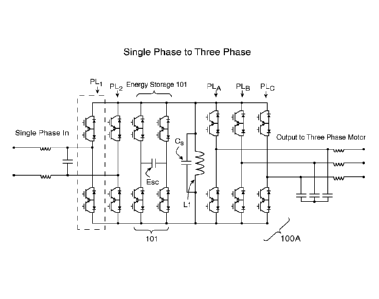
[000124] Figure 27 shows a sample embodiment as a single phase
to three phase synchronous motor drive, as may be used for driving a
household air-conditioner compressor at variable speed, with unity power
factor and low harmonics input. Delivered power is pulsating at twice the
input power frequency.
[000125] Figure 28 shows a sample embodiment with dual,
parallel power modules, with each module constructed as per the converter
of Figure 1, excluding the I/O filtering. This arrangement may be
advantageously used whenever the converter drive requirements exceed that
obtainable from a singe power module and/or when redundancy is desired
for reliability reasons and/or to reduce I/O filter size, so as to reduce
costs,
losses, and to increase available bandwidth. The power modules are best
operated in a manner similar to multi-phase DC power supplies such that the
link reactance frequencies are identical and the current pulses drawn and
CA 02808490 2014-09-18
34
supplied to the input/output filters from each module are uniformly spaced in
time. This provides for a more uniform current draw and supply, which may
greatly reduce the per unit filtering requirement for the converter. For
example, going from one to two power modules, operated with a phase
difference of 90 degrees referenced to each of the modules
inductor/capacitor, produces a similar RMS current in the I/O filter
capacitors, while doubling the ripple frequency on those capacitors. This
allows the same I/O filter capacitors to be used, but for twice the total
power, so the per unit I/O filter capacitance is reduced by a factor 2. More
importantly, since the ripple voltage is reduced by a factor of 2, and the
frequency doubled, the input line reactance requirement is reduced by 4,
allowing the total line reactor mass to drop by 2, thereby reducing per unit
line reactance requirement by a factor of 4.
[000126] Figure 29 shows an embodiment as a three phase Power
Line Conditioner, in which role it may act as an Active Filter and/or supply
or absorb reactive power to control the power factor on the utility lines. If
a
battery, with series inductor to smooth current flow, is placed in parallel
with the output capacitor 2901, the converter may then operate as an
Uninterruptible Power Supply (UPS).
[000127] According to some (but
not necessarily all) disclosed
embodiments, there is provided: A Buck-Boost Converter, comprising: an
energy-transfer reactance; first and second power portals, each with two or
more ports by which electrical power is input from or output to said portals;
first and second bridge switch arrays interposed between said reactance and
respective ones of said portals, and each comprising one bidirectional
switching device for each said port of each said power portal; an an energy
CA 02808490 2014-09-18
storage capacitor, reversibly connected across said reactance through a
bridge configuration.
[000128] According to some (but
not necessarily all) disclosed
embodiments, there is provided: A Buck-Boost Converter, comprising: an
energy-transfer reactance; a first bridge switch array comprising at least two
bidirectional switching devices which are jointly connected to operatively
connect at least one terminal of said reactance to a power input, with
reversible polarity of connection; a second bridge switch array comprising at
least two bidirectional switching devices which are jointly connected to
operatively connect at least one terminal of said reactance to a power output,
with reversible polarity of connection; and an energy storage capacitor,
reversibly connected across said reactance through a full-bridge
configuration; wherein said first switch array drives said reactance with a
nonsinusoidal voltage waveform.
[000129] According to some (but
not necessarily all) disclosed
embodiments, there is provided: A Full-Bridge Buck-Boost Converter,
comprising: first and second full bridge switch arrays, each comprising at
least four bidirectional switching devices; a substantially parallel inductor-
capacitor combination symmetrically connected to be driven separately by
either said switch array; and an energy storage capacitor, reversibly
connected across said reactance through a full-bridge configuration; one of
said switch arrays being operatively connected to a power input, and the
other thereof being operatively connected to supply a power output.
[000130] According to some (but
not necessarily all) disclosed
embodiments, there is provided: A Buck-Boost Converter, comprising: first
and second switch arrays, each comprising at least two bidirectional
CA 02808490 2014-09-18
36
switching devices; a substantially parallel inductor-capacitor combination
connected to each said switch array; and an energy storage capacitor,
reversibly connected across said reactance through a full-bridge
configuration; wherein a first one of said switch arrays is operatively
connected to a power input, and is operated to drive power into said
inductor- capacitor combination with a non-sinusoidal waveform; and
wherein a second one of said switch arrays is operated to extract power from
said inductor-capacitor combination to an output.
[000131] According to some (but not necessarily all) disclosed
embodiments, there is provided: A power conversion circuit, comprising: an
input stage which repeatedly, at various times, drives current into the
parallel
combination of an inductor and a capacitor, and immediately thereafter
temporarily disconnects said parallel combination from external
connections, to thereby transfer some energy from said inductor to said
capacitor; wherein said action of driving current is performed in opposite
senses at various times, and wherein said disconnecting operation is
performed substantially identically for both directions of said step of
driving
current; an energy storage capacitor, reversibly connected across said
reactance through a full-bridge configuration; and an output stage which
extracts energy from said parallel combination, to thereby perform power
conversion.
[000132] According to some (but not necessarily all) disclosed
embodiments, there is provided: A method for operating a Buck-Boost
Converter, comprising the actions of: (a) operating a first bridge switch
array, comprising bidirectional switching devices, to operatively connect at
least one terminal of a reactance to a power input, with polarity which
CA 02808490 2014-09-18
37
reverses at different times; (b) operating a second bridge switch array,
comprising bidirectional switching devices, to operatively connect at least
one terminal of said reactance to a power output, with polarity which
reverses at different times; (c) operating an H-bridge switch subarray to
operatively connect an energy storage capacitor to said reactance at various
times, with polarity which reverses at various times, to provide net energy
transfer into and out of said energy storage capacitor; and wherein said
actions (a) and (b) are not performed simultaneously.
[000133] According to some (but
not necessarily all) disclosed
embodiments, there are provided: Methods and systems for power
conversion. An energy storage capacitor is contained within an H-bridge
subcircuit which allows the capacitor to be connected to the link inductor of
a Universal Power Converter with reversible polarity. This provides a
"pseudo-phase" drive capability which expands the capabilities of the
converter to compensate for zero-crossings in a single-phase power supply.
Modifications and Variations
[000134] As will be recognized
by those skilled in the art, the
innovative concepts described in the present application can be modified and
varied over a tremendous range of applications, and accordingly the scope of
patented subject matter is not limited by any of the specific exemplary
teachings given. It is intended to
embrace all such alternatives,
modifications and variations that fall within the spirit and broad scope of
the
appended claims.
CA 02808490 2014-09-18
38
[000135] The sizing of ESC is independent of the sizing of the link
inductor. Typically 25% to about 50% of total energy transferred goes
through the ESC, but this percentage can vary significantly depending on the
application.
[000136] In general it is only necessary to have one energy storage
capacitor in the circuit. However, it is also possible (less preferably) to
have
more than one energy storage capacitor.
[000137] In a multiport system, it is usually most efficient to locate
the energy-storage capacitor on the highest-voltage port of the system.
However, this can be varied.
[000138] None of the description in the present application should
be read as implying that any particular element, step, or function is an
essential element which must be included in the claim scope: THE SCOPE
OF PATENTED SUBJECT MATTER IS DEFINED ONLY BY THE
ALLOWED CLAIMS.
[000139] The claims as filed are intended to be as comprehensive
as possible, and NO subject matter is intentionally relinquished, dedicated,
or abandoned.