Note: Descriptions are shown in the official language in which they were submitted.
81779663
SPECIFICATION
Title of the Invention: Eyeglass lens
CROSS-REFERENCE TO RELATED APPLICATIONS
[0001] This application claims priority to Japanese Patent Application No.
2012-217200 filed on September 28, 2012 and Japanese Patent Application No.
2012-217204 filed on September 28, 2012.
TECHNICAL FIELD
[0002] The present invention relates to an eyeglass lens, and more
particularly, to an
eyeglass lens having a vapor-deposited film that can exhibit good heat
resistance (crack
resistance) and scratch resistance.
BACKGROUND ART
[0003] Generally, eyeglass lenses are imparted with various properties by
forming
various functional films on the lens substrate while achieving a desired
refractive index
by means of the lens substrate. Antireflective films imparting an
antireflective property
to the lens surface are widely employed as such functional films. Among these,
vapor-deposited films of zirconium (Zr) oxide are inexpensive among the high
refractive index layers constituting multilayer antireflective films, and are
thus
considered advantageous in terms of cost (for example, see Japanese Unexamined
Patent Publication (KOKAI) No. 2009-193022).
Vapor-deposited films of tantalum (Ta) oxide can also
function as high refractive index layers in the same way as vapor-deposited
films of
zirconium oxide.
[0004] Eyeglass lenses are required to have good durability that does not
deteriorate
1
CA 2889741 2018-09-28
CA 02889741 2015-04-27
even when placed in various environments. For example, eyeglass lenses are
sometimes
worn in the bath, left in automobiles in summer, and worn by wearers who are
active for
extended periods outdoors. There is a need for them to maintain good quality
without
developing cracks even when exposed to such elevated temperatures. In eyeglass
lenses
having vapor-deposited films of zirconium oxide and tantalum oxide, cracks may
develop in the vapor-deposited films at elevated temperatures, resulting in
phenomena
such as a drop in optical characteristics and decreased adhesion between
layers
constituting the multilayer antireflective film.
[0005] Eyeglass lenses are also required to have good resistance to scratching
without
developing scratches or cracks with the application of external forces.
Eyeglass lenses
are subjected to various external forces in the course of removing
fingerprints, debris,
and other grime adhering to the lens surface. The scratches and cracks that
develop due
to such external forces cause phenomena such as decreased optical
characteristics in the
eyeglass lens and diminished adhesion between layers constituting multilayer
antireflective films.
SUMMARY OF THE INVENTION
[0006] An aspect of the present invention provides for an eyeglass lens having
a
zirconium oxide or tantalum oxide vapor-deposited film and having good heat
resistance (crack resistance) and scratch resistance.
[0007] The present inventors discovered the following previously unknown
matters in
the course of conducting extensive research into achieving the above eyeglass
lens:
(1) The greater the uniformity in the planar TEM image of the above metal
oxide
vapor-deposited film, the better the heat resistance and the fewer cracks
generated at
elevated temperatures;
2
CA 02889741 2015-04-27
(2) The greater the uniformity in the planar TEM image of the above metal
oxide
vapor-deposited film, the greater the compressive stress, such that even when
external
forces were applied, forces counteracting them were produced, resulting in
good scratch
resistance and the generation of few scratches or cracks due to external
forces.
(3) For the grains determined in the planar TEM image, since the presence of
numerous
small grains reduces uniformity, the larger the size (grain size) the higher
the uniformity
of the film.
NOON The fact that the uniformity of the above planar TEM image is high and
the
grain size is large is an indicator of low anisotropy and high uniformity in
the planar
direction of the above vapor-deposited film. That is, the fact that decreasing
the
anisotropy and increasing the uniformity in the planar direction made it
possible to
increase the heat resistance and scratch resistance of the above vapor-
deposited film was
discovered by the present inventors.
Based on the above discoveries, the present inventors adopted the grain size
and uniformity of the planar TEM image as new indicators and conducted
repeated
research by trial and error, varying the manufacturing conditions of the vapor-
deposited
film of the above metal oxide and the like. This resulted in the discovery
that an oxide
film of metal selected from the group consisting of zirconium and tantalum,
having an
average grain size of equal to or greater than 3.5 mu in a planar TEM image
thereof and
having a proportion accounted for by grain boundaries, which are boundaries
separating
grains from regions outside of the grains, of less than 15%, will have a high
heat
resistance and will not develop cracks (or develop few cracks) even when
placed under
high temperature, and will have good scratching resis ance. The present
invention was
developed on that basis.
3
81779663
[0009] An aspect of the present invention relates to an eyeglass lens
comprising a lens
substrate and a vapor-deposited film either directly or indirectly on the lens
substrate, wherein
the vapor-deposited film is an oxide film of metal selected from the group
consisting of zirconium and tantalum, with an average grain size observed in a
planar image
obtained by a transmission electron microscope of equal to or greater than 3.5
nm and a
proportion accounted for by grain boundaries, which are boundaries separating
grains from
regions outside of the grains, in a planar image obtained by a transmission
electron
microscope of less than 15%.
[0009a] A further aspect of the present invention relates to an eyeglass lens
comprising a lens
substrate and a vapor-deposited film either directly or indirectly on the lens
substrate, wherein
the vapor-deposited film is an oxide film of zirconium, with an average grain
size observed in a planar image obtained by a transmission electron microscope
ranging from
3.5 nm to 20 nm and a proportion accounted for by grain boundaries, which are
boundaries
separating grains from regions outside of the grains, in a planar image
obtained by a
transmission electron microscope of equal to or greater than 1% and less than
15% based on
the entire area of the observed field, which is set to 100 nm square (100 nm x
100 nm) to
150 nm square (150 nm x 150 nm) at a magnification of 100,000 to 200,000-fold,
or 50 nm
square (50 nm x 50 nm) to 100 nm square (100 nm x 100 nm) at a magnification
of exceeding
200,000-fold.
[0010] In an embodiment, the proportion accounted for by regions observed in a
streaky
shape, in a columnar shape, or in a lump shape in a cross-sectional image of
the vapor-
deposited film obtained by a transmission electron microscope is less than
55%.
[0011] In an embodiment, the above vapor-deposited film is a zirconium oxide
film.
4
CA 2889741 2018-09-28
81779663
[0012] In an embodiment, the above eyeglass lens comprises the above vapor-
deposited film
as at least one layer in a multilayer vapor-deposited film.
[0013] A further aspect of the present invention relates to a method of
determining a
manufacturing condition of an eyeglass lens comprising a vapor-deposited film
that is an
oxide film of metal selected from the group consisting of zirconium and
tantalum, which
comprises:
determining a candidate vapor deposition condition to be employed in vapor
deposition of the vapor-deposited film in actual manufacturing;
forming a test vapor-deposited film by conducting vapor deposition under the
candidate vapor deposition condition that has been determined; and
taking at least one TEM image selected from the group consisting of a planar
4a
CA 2889741 2018-09-28
CA 02889741 2015-04-27
TEM image or a cross-sectional TEM image the test vapor-deposited film that
has been
formed and determining a vapor deposition condition of the vapor-deposited
film in
actual manufacturing, with a determination standard that the higher the
uniformity of
the TEM image, the more likely the candidate condition is to be a vapor
deposition
condition capable of forming a vapor-deposited film exhibiting good heat
resistance or
good scratch resistance, or good heat resistance and good scratch resistlance.
[0014] In an embodiment, the uniformity is determined according to at least
one
determination standard selected from the group consisting of standards 1 to 4
below:
standard 1: in a cross-sectional TEM image, the lower the proportion accounted
for by
regions observed in a streaky shape, in a columnar shape, or in a lump shape,
or the
smaller the regions, the higher the uniformity is determined to be;
standard 2: the greater the area of dark portions obtained by binary
processing of a
cross-sectional TEM image obtained as a bright-field image, or the greater the
area of
the bright portions obtained by binary processing of a cross-sectional IBM
image
obtained as a dark-field image, the higher the uniformity is determined to be;
standard 3: the lower the proportion accounted for by grain boundaries in a
planar TEM
image, the higher the uniformity is determined to be; and
standard 4: the greater the grain size observed in a planar TEM image, the
higher the
uniformity is determined to be.
[0015] A further aspect of the present invention relates to a method of
manufacturing
an eyeglass lens, which comprises:
determining a manufacturing condition by the method set forth above; and
conducting vapor deposition under the manufacturing condition that has been
determined to form a vapor-deposited film in the form of an oxide film of
metal selected
CA 02889741 2015-04-27
=
from the group consisting of zirconium and tantalum.
[0016] In an embodiment, the above vapor-deposited film is formed as a layer
constituting a multilayer antirefiective film.
[0017] An aspect of the present invention can provide an eyeglass lens having
good
durability in which the generation of cracks in the vapor-deposited film ¨
which is an
oxide film of metal selected from the group consisting of zirconium and
tantalum ¨ at
high temperature and the occurrence of scratches and cracks due to external
forces are
inhibited.
Brief Description of Drawings
[0018] [Figure 1] A descriptive drawing of a method of measuring film stress.
[Figure 2] A descriptive drawing of a method of measuring film stress.
[Figure 3] Figure 3 is a cross-sectional TEM image obtained for Example 1.
[Figure 4] Figure 4 is a planar TEM image obtained for Example 1.
[Figure 5] Figure 5 is a cross-sectional TEM image obtained for Example 2.
[Figure 6] Figure 6 is a planar 1EM image obtained for Example 2.
[Figure 7] Figure 7 is a cross-sectional TEM image obtained for Example 3.
[Figure 8] Figure 8 is a planar TEM image obtained for Example 3.
[Figure 9] Figure 9 is a planar TEM image obtained for Example 4.
[Figure 10] Figure 10 is a cross-sectional TEM image obtained for Comparative
Example 1.
[Figure 111 Figure 11 is a planar FEM image obtained for Comparative Example
2.
[Figure 12] Figure 12 is a partial enlargement within a frame of the grain of
the planar
IEM image shown in Figure 11.
MODES FOR CARRYING OUT THE INVENTION
6
CA 02889741 2015-04-27
[0019] An aspect of the present invention relates to an eyeglass lens
comprising a lens
substrate and a vapor-deposited film either directly or indirectly on the lens
substrate,
wherein the vapor-deposited film is an oxide film of metal selected from the
group
consisting of zirconium and tantalum, with an average grain size (referred to
as the
"average grain size", hereinafter) observed in a planar image obtained by a
transmission
electron microscope (planar TEM image) of equal to or greater than 3.5 nm and
a
proportion (referred to as the "grain boundary occupancy rate", hereinafter)
accounted
for by grain boundaries, which are boundaries separating grains from regions
outside of
the grains, in a planar image obtained by a transmission electron microscope
of less than
15%. Eyeglass lenses in which no grains are observed, that is, with the oxide
film of
metal selected from the group consisting of zirconium and tantalum having a
proportion
accounted for by grain boundaries of 0%, are also included in the eyeglass
lens
according to an aspect of the present invention.
The eyeglass lens according to an aspect of the present invention will be
described in greater detail below.
[0020] The eyeglass lens has a vapor-deposited film in the form of an oxide
film of
metal selected from the group consisting of zirconium and tantalum, either
directly or
indirectly on the lens substrate. The zirconium oxide film will be denoted as
a "Zr oxide
film" and the tantalum oxide film as a "Ta oxide film" hereinafter. The lens
substrate is
not specifically limited. Materials that are commonly employed as the lens
substrates of
eyeglass lenses, such as materials selected from among polyurethane,
polythiourethane,
polycarbonate, diethyleneglycol bisallylcarbonate, other plastics, and
inorganic glass,
can be employed. The thickness and diameter of the lens substrate are normally
a
thickness of about 1 to 30 mm and a diameter of about 50 to 100 mm, but there
is no
7
CA 02889741 2015-04-27
specific limitation.
[0021] As set forth above, Zr oxide films and Ta oxide films can function as
high
refractive index layers. They can be used to form a single layer on the lens
substrate, or
combined with layers of different refractive indexes, such as a low refractive
index layer
formed primarily of SiO2 to form multilayer vapor-deposited films provided in
the lens
substrate. Such multilayer vapor-deposited films can further contain single-
layer or two
or more vapor-deposited films (also called "electrically conductive oxide
layers")
formed by vapor deposition using vapor deposition sources primarily comprised
of an
electrically conductive oxide. Providing such an electrically conductive oxide
layer can
prevent the adhesion of dust and debris on the lens surface. The electrically
conductive
oxide is desirably in the form of a known indium oxide, tin oxide, or zinc
oxide, or
some compound oxide thereof, that is known as a transparent electrically
conductive
oxide so as not to reduce the transparence of the eyeglass lens. From the
perspective of
transparence and electrical conductivity, a preferred example of an
electrically
conductive oxide is an indium-tin oxide (ITO). An embodiment of the multilayer
vapor-deposited film is an antireflective film. However, there is no
limitation to
antireflective films. Any such layer that functions as a reflecting layer
(cutting layer)
performing the function of reducing the amount of light entering the eye of
the eyeglass
wearer by selectively reflecting light of a prescribed wavelength range will
do. An
example of light that is desirably reflected is ultraviolet light. The short
wavelength
light known as blue light that is emitted by the liquid crystal monitors that
have become
widespread in recent years, particularly the light emitted at a wavelength of
roughly 400
rim to 500 nm by LED liquid-crystal monitors, is another example.
[0022] The thickness of the Zr oxide or Ta oxide film can be a physical film
thickness
8
CA 02889741 2015-04-27
of about 10 to 100 nm, for example. It suffices to determine the film
thickness based on
the function (antireflective property or the like) that is required of the
film; there is no
specific limitation. The film thicknesses given below refer to physical film
thicknesses.
[0023] The eyeglass lens according to an aspect of the present invention
comprises
one or more layers of Zr oxide film or Ta oxide film on a lens substrate.
These oxide
films can be optionally combined into two or more layers. At least one layer
of Zr oxide
film or Ta oxide film is a vapor-deposited film with an average grain size
observed in a
planar TEM image of equal to or greater than 3.5 nm and a proportion (grain
boundary
occupancy rate) accounted for by grain boundaries, which are boundaries
separating
grains from regions outside of the grains, in a planar image obtained by a
transmission
electron microscope of less than 15%. The planar TEM image is obtained by
observing the vapor-deposited film that is the subject of observation by a
transmission
electron microscope (TEM) in a direction that is perpendicular to, or
approximately
perpendicular to, the direction of thickness. By contrast, the method of
observation in
a direction that is parallel or approximately parallel to the direction of
thickness is
cross-sectional TEM observation. This point will be described further below.
Through
research, the present inventors discovered that the higher the uniformity of
the planar
TEM image, the greater the heat resistance (crack resistance) and scratch
resistance. The
grain boundary occupancy rate and the average grain size observed in the
planar TEM
image is adopted as an indicator of uniformity in an aspect of the present
invention.
Based on investigation conducted by the present inventors, in elemental
analysis
conducted by TEM-EDS, for example, no clear difference was observed between
films
with different heat resistance (crack resistance) and scratch resistance for
Zr oxide films
and Ta oxide films. Thus, the specific correlation between the heat resistance
(crack
9
CA 02889741 2015-04-27
resistance) and scratch resistance of Zr oxide films and Ta oxide films of
different
uniformity in their plann TEM images was discovered by the present inventors.
The
planar TEM image is obtained in the present invention by known methods in
which a
transmission electron microscope is employed.
[0024] In the above Zr oxide film and Ta oxide film, the average grain size
observed
in the planar image (planar TEM image) obtained by a transmission electron
microscope
is equal to or greater than 3.5 nm as stated above, desirably equal to or
greater than 5
nm, preferably equal to or greater than 5.5 nm, and yet more preferably, equal
to or
greater than 5.8 nm. The average size is, for example, equal to or less than
20 nm, but
the larger the grain size the better, since the presence of multiple minute
grains
decreases the uniformity of the film. The proportion accounted for in the
planar TEM
image by grain boundaries separating grains from regions outside of the grains
is less
than 15% as set forth above, desirably equal to or less than 10%, preferably
equal to or
less than 5%, and more preferably, equal to or less than 3%. The smaller, the
better.
[0025] The grains that are observed in the planar TEM image are observed as
regions
that are enclosed by grain boundaries and thus separated from other regions in
a planar
TEM image obtained at a magnification of 50,000 to 400,000-fold. The grain
boundaries can be identified by differences in shading in the TEM image. The
proportion of the entire area of the observed field that is accounted for by
grain
boundaries falls within the range stated above. The observed field can be set
to permit
clear determination of the separation of the grains from the regions outside
of the grains
by means of grain boundaries, based on the size of grains observed in the
planar TEM
image. The observed field can be set to a range, for example, of 50 nm square
(50 urn x
50 nin) to 150 nm square (150 nm x 150 nm). For example, an observed field at
a
CA 02889741 2015-04-27
=
magnification of 100,000 to 200,000-fold can be set to 100 nm square (100 tun
x 100
nm) to 150 nm square (150 nm x 150 nm), and an observed field exceeding a
magnification of 200,000-fold can be set to 50 nm square (50 nm x 50 nm) to
100 nm
square (100 nm x 100 nm). The observation position is desirably changed to
obtain
TEM images at five or more spots (for example, 5 to 10 spots), and grain
boundary
occupancy rates are desirably obtained as the arithmetic average value of the
measurement values obtained from the various TEM images.
[0026] The planar TEM image can be obtained as a bright-field image or as a
dark-field image. From the perspective of ease of analysis, it is desirable to
obtain a
planar TEM image in the form of a dark-field image when microcrystals are
contained.
Conversely, it is desirable to obtain the planar TEM image in the form of a
bright-field
image when considerable amorphous materials are present.
[0027] The grains that are observed in the planar TEM image are distinguished
from
other regions by the grain boundaries, and are primarily regions determined to
be
granular or in a cluster shape, but can also be of indeterminate shape.
Examples of the
specific structures of the grains are structures within which crystalline
grains are present
in the grains. The grains can contain one or both of crystals and amorphous
materials.
The presence of crystals can be determined by observing the crystal lattice.
The average
grain size in the planar TEM image that is referred to can be either a value
that is
calculated by measuring the major axis and minor axis of each region
distinguished as
another region by the grain boundaries in the observed field, calculating the
average
value of the major axes and the average value of the minor axes of the lump
regions
contained in the observed field, and adopting the value obtained by
calculating (major
axis average value + minor axis average value)/2. Alternatively, the diameter
of a circle
11
CA 02889741 2015-04-27
having the same area as each of the regions, that is, the equivalent circle
diameter, is
calculated for the grains that are contained in the observed field, and the
average value
is adopted as the average grain size. Grains with portions that protrude from
the image
are not measured. The average value is the arithmetic average. When numerous
grains
are observed, the area of the observed field can be changed to contain 50 or
more
(desirably 100 or more) grains, for example. When indeterminate grains are
contained,
in cases where their shapes are small or their crystallinity is high, the
observation region
can be expanded (for example, a 100,000-fold field can be expanded to a 200%
image)
and compared with results obtained from an observation image that has been
separately
observed at high magnification (for example, 200,000-fold, 250,000-fold, or
400,000-fold). When the value of the results of comparison differs by 1 nm or
more, the
average value is desirably adopted. The average grain size is desirably
measured at
five or more spots (for example, 5 to 10 spots) by changing the observation
position and
obtaining an average value, as set forth above for the gain boundary occupancy
rate.
Reference can be made to JIS R 1670: 2006 for measurement of the average
grain size set forth above.
[0028] In a desirable embodiment, in the Zr oxide film and Ta oxide film, the
proportion accounted for by regions observed in a streaky shape, in a columnar
shape,
or in a lump shape in a cross-sectional image (cross-sectional TEM image)
obtained by
a transmission electron microscope is less than 55%, preferably equal to or
less than
40%, more preferably equal to or less than 30%, still more preferably equal to
or less
than 15%, yet more preferably equal to or less than 10%, and yet still more
preferably
equal to or less than 5%. The proportion accounted for by regions in a lump
shape is
desirably small.
12
CA 02889741 2015-04-27
[0029] The above regions observed in the cross-sectional TEM image are
observed as
regions distinguished from the other regions by different shades in a cross-
sectional
TEM image obtained at a magnification of 50,000 to 400,000-fold. Normally,
these
regions are observed with a nonuniform, marbled structure in a cross-sectional
TEM
image. The proportion accounted for by these regions is desirably obtained by
changing the observation position and calculating the arithmetic average
values of five
or more spots (for example, 5 to 10 spots), as set forth above for the
observation of the
planar TEM image. The details of obtaining and analyzing cross-sectional TEM
images
are identical to those set forth regarding the planar TEM images above.
[0030] The cross-sectional TEM image can be obtained as a bright-field image
or as a
dark-field image. From the perspective of facilitating analysis, the cross-
sectional TEM
image is desirably obtained in the form of a dark-field image for those
containing
microcrystals. On the other hand, when considerable amorphous materials are
present,
the cross-sectional FBM image is desirably obtained as a bright-field image.
[0031] The above regions observed in the cross-sectional TEM image are, as set
forth
above, observed in a streaky shape, in a columnar shape, or in a lump shape,
and may be
indeterminate forms. Examples of specific structures that can be contained in
these
regions are columnar structures and crystalline grains. Columnar structures
are mainly
determined in a direction normal to, or approximately normal to, the surface
of the lens
substrate (base material). Crystalline grains are mainly determined as grains
or in a state
in which they are arranged in columns in a direction normal to, or
approximately normal
to, the lens substrate. The term "in a direction approximately normal to" is
used to mean
including directions inclined by about 20 when the normal direction is
denoted as 0 .
Columnar structures and crystalline grains may include amorphous materials in
addition
13
CA 02889741 2015-04-27
to crystals. The incorporation of crystals can be determined by the
observation of the
crystal lattice in the LW image.
[0032] Desirably, the above-described Zr oxide film can be formed by vapor
deposition of a vapor deposition source the primary component of which is ZrO2
and
the Ta oxide film can be formed by vapor deposition of a vapor deposition
source the
primary component of which is Ta205. In an aspect of the present invention,
the
"primary component" refers to the component accounting for the greatest
portion of the
vapor deposition source or the vapor deposition layer. This component normally
accounts for about 50 mass percent to 100 mass percent of the total, even
about 90 mass
percent to 100 mass percent. Impurities that inevitably mix in in trace
amounts will
sometimes be contained in the vapor deposition source. Other components can be
contained in ranges that do not compromise functioning of the primary
component, such
as other inorganic substances and known additive components that play
assisting roles
in vapor deposition. Vapor deposition can be conducted by vacuum vapor
deposition,
ion plating, plasma CVD, the ion-assisted method, reactive sputtering, or the
like. The
ion-assisted method is desirable for obtaining good adhesion.
[0033] For example, in the ion-assisted method, it is possible to control the
physical
properties of the vapor-deposited film that is formed by means of the vapor
deposition
conditions, such as the degree of vacuum, acceleration voltage, acceleration
current,
assist gas (ionized gas) flow rate and blending ratio during vapor deposition,
as well as
the composition and the like of the vapor deposition source employed. In an
embodiment of the present invention, the vapor deposition conditions can be
determined
by conducting preliminary testing as needed to form the above Zr oxide film
and Ta
oxide film.
14
CA 02889741 2015-04-27
[0034] In the field of manufacturing eyeglass lenses, to stably provide
eyeglass lenses
of a quality that does not decrease over time, prior to determining the
conditions used in
actual manufacturing, it is common practice to conduct accelerated durability
testing on
test sample eyeglass lenses that have been fabricated using candidate
manufacturing
conditions and adopt, in actual manufacturing, manufacturing conditions that
are
identical to the manufacturing conditions of the test sample eyeglass lenses
that have
exhibited good test results. For example, by forming vapor-deposited films in
actual
manufacturing under manufacturing conditions that have yielded test sample
eyeglass
lenses with few cracks in accelerated durability testing by oven heating, it
is possible to
obtain eyeglass lenses exhibiting good durability without undergoing
deterioration of
the vapor-deposited film over extended periods of actual use.
Further, to stably provide high-quality eyeglass lenses, prior to determining
conditions for actual manufacturing, it is common practice to conduct
performance
evaluation tests on test sample eyeglass lenses fabricated under candidate
manufacturing
conditions and adopt manufacturing conditions identical to the manufacturing
conditions of test sample eyeglass lenses exhibiting good test results in
actual
manufacturing. For scratch resistance, by forming vapor-deposited films in
actual
manufacturing by manufacturing conditions that have yielded test sample
eyeglass
lenses producing few cracks in scratch tests in which loads are placed on
steel wool or a
sand eraser, for example, it is possible to obtain eyeglass lenses exhibiting
good
durability with little scratch or crack generation in actual use.
[0035] Although the above accelerated durability test has become indispensable
to
providing eyeglass lenses exhibiting good durability for extended periods and
with high
reliability, in order to manufacture eyeglass lenses that currently pass
accelerated
CA 02889741 2015-04-27
durability tests, candidate vapor deposition conditions are determined for
manufacturing
product eyeglass lenses, eyeglass lenses are fabricated by forming vapor
deposition
films under the vapor deposition conditions that have been determined, and the
eyeglass
lenses that have been fabricated are subjected to accelerated durability
testing. When the
evaluation standards are not satisfied, new candidate vapor deposition
conditions are
selected and the series of steps are repeated in a process of trial and error.
Even though
the scratch resistance test employing test sample eyeglass lenses set forth
above has
become indispensable for providing eyeglass lenses exhibiting good scratch
resistance
over extended periods with high reliability, in order to manufacture eyeglass
lenses that
currently pass scratch resistance tests, candidate vapor deposition conditions
are
determined for manufacturing product eyeglass lenses, eyeglass lenses are
fabricated by
forming vapor deposition films under the vapor deposition conditions that have
been
determined, and the eyeglass lenses that have been fabricated are subjected to
scratch
resistance testing. When the evaluation standards are not satisfied, new
candidate vapor
deposition conditions are selected and the series of steps are repeated in a
process of
trial and error.
By contrast, by conducting evaluation based on a TEM image selected from the
group consisting of the planar TEM image and the cross-sectional 11,M image in
the
manner discovered by the present inventors, manufacturing conditions for Zr
oxide
films and Ta oxide films, in which the generation under high temperatures can
be
inhibited and good scratch resistance can be achieved, can be readily
discovered.
[0036] In an embodiment, candidate vapor deposition conditions for a vapor-
deposited
film are first determined for the manufacturing of a product lens. For
example, when
using the ion-assisted method in actual manufacturing, the above various
conditions are
16
CA 02889741 2015-04-27
=
determined. When using some other vapor deposition method, the various
conditions
relating to that vapor deposition method are determined.
[0037] Next, vapor deposition is conducted under the vapor deposition
conditions that
have been determined as set forth above and a test vapor deposition film is
fabricated.
The test vapor deposition film can be formed on the lens substrate or on the
surface of a
functional film on the lens substrate in the same manner as in actual
manufacturing, or
formed on a test substrate of glass or the like. From the perspective of ease
of IEM
observation, it is desirable to fabricate the test vapor deposition film on a
glass
substrate.
[0038] The test vapor deposition film fabricated as set forth above is
observed by
TEM selected from the group consisting of planar 11M observation and cross-
sectional
TEM observation. The details of the TEM observation are as set forth above.
[0039] In determining the uniformity of a cross-sectional TEM image, for
example,
cross-sectional TEM images are visually compared. Images in which marbled
nonuniform structures are found are determined to poor uniformity and images
in which
such structures are not found are determined to be highly uniform.
Uniformity can be determined based on standard 1, standard 2, or standards 1
and 2 below.
Standard 1: in a cross-sectional TEM image, the lower the proportion accounted
for by
regions observed in a streaky shape, in a columnar shape, or in a lump shape,
or the
smaller the regions, the higher the uniformity is determined to be.
Standard 2: the greater the area of dark portions obtained by binary
processing of a
cross-sectional TEM image obtained as a bright-field image, or the greater the
area of
the bright portions obtained by binary processing of a cross-sectional TEM
image
17
CA 02889741 2015-04-27
=
obtained as a dark-field image, the higher the uniformity is determined to be.
[0040] As an example of the regions observed in a streaky shape, in a columnar
shape,
or in a lump shape in evaluation by standard 1, in a cross-sectional TEM image
obtained
at a magnification of 150,000-fold, the region the major diameter (major axis
length) of
which based on differences in shading is equal to or greater than 1 nm as an
actual size
is identified as the above region, and the presence of such regions can be
determined.
The size of the above regions can be determined manually by a person or
determined
automatically by software analysis. For example, the determination of standard
1 can be
conducted based on the major axis length and minor axis length of one or more
such
regions (with a columnar structure, for example) in a cross-sectional TEM
image, or
based on the average value of the size of multiple such regions.
[0041] The binary processing of standard 2 can be conducted in the manner
below, for
example.
The brightness of each pixel (picture element) of a cross-sectional TEM image
that has been obtained and the average brightness of the entire image are
obtained. The
ratio of the number of pixels that are brighter than the average relative to
the entire
number of pixels is adopted as the area fraction of the bright portion, and
the ratio of the
number of pixels that are darker than the average relative to the entire
number of pixels
is adopted as the area fraction of the dark portion, and the area of the
bright portion and
the dark portion can be obtained. More specifically, the gradation of each
pixel is
obtained for a common digital image file (gray scale, for example, 256
gradations), a
histogram is prepared from the number of pixels and the gradation, and the
average
gradation of the image as a whole is obtained. Binary processing is conducted
with the
average gradation as a threshold, with pixels with gradations (bright) greater
than or
18
CA 02889741 2015-04-27
=
equal to the threshold being assigned the value 1 and pixels with gradations
(dark)
below the threshold being assigned the value 0. For the entire number of
pixels, the
number of pixels with a value of 1 is calculated, and this number is adopted
as the
bright area fraction.
Such binary processing can be automatically carried out with known analysis
software.
[0042] The uniformity of a planar TEM image can be determined by, for example,
comparing the analysis results of planar TEM images visually or with analysis
software,
determining that those images in which the proportion accounted for by grain
boundaries is large are of poor uniformity, and determining that those images
in which
this proportion is small are of high uniformity (standard 3). The larger the
grain size
observed in a planar TEM image, the higher the uniformity is determined to be
(standard 4). The grain size used in making the determination can be measured
manually by a person or automatically with analysis software.
[0043] As set forth further below, the difference in uniformity of TEM images
determined as set forth above correlates with the heat resistance (crack
resistance) of the
vapor-deposited film. The present inventors have confirmed that the higher the
uniformity, the less cracking occurs at elevated temperatures. Accordingly, in
an
embodiment, the vapor deposition conditions of the vapor-deposited film in
actual
manufacturing are determined based on a standard of determining that candidate
conditions of high uniformity in a TEM image are vapor deposition conditions
permitting the formation of a vapor-deposited film exhibiting good heat
resistance.
As set forth further below, the present inventors have confirmed that the
difference in uniformity of TEM images determined as set forth above
correlates with
19
CA 02889741 2015-04-27
=
the magnitude of compressive stress on the vapor-deposited film. The highter
the
uniformity, the greater the compressive stress, such that even when external
forces are
applied, a force counteracting them is generated, resulting in good scratch
resistance.
Accordingly, in an embodiment, the vapor deposition conditions for the vapor-
deposited
film in actual manufacturing are determined based on a standard of determining
that
candidate conditions of high uniformity in a TEM image are vapor deposition
conditions that permit the formation of a vapor-deposited film exhibiting good
scratch
resistance.
For example, in a specific implementation mode, it is possible to determine
actual manufacturing conditions based on a relative determination of adopting
vapor
deposition conditions for a vapor-deposited film in actual manufacturing in
the form of
the conditions with the highest uniformity in their TEM images among two or
more sets
of candidate conditions.
Further, in another specific implementation mode, preliminary testing is
conducted, and a data base is created of correlations between vapor deposition
conditions of vapor-deposited films and the tendency for cracks to develop at
high
temperature and the tendency for scratches and cracks to develop due to
external forces.
Based on the data base, a uniformity threshold (critical value) permitting the
formation
of vapor-deposited films with good heat resistance and scratch resistance is
set. Films
having uniformity higher than or equal to the threshold can then be used to
determine
the vapor deposition conditions of vapor-deposited films in actual
manufacturing. The
grain size or grain boundary occupancy rate in a planar TEM image, the bright
portion
or dark portion area fraction obtained by binary processing in a cross-
sectional TEM
image, the major axis length or minor axis length of the above regions, or the
like can
CA 02889741 2015-04-27
=
be employed as the threshold.
For example, for a cross-sectional TEM image, the area fraction of the dark
portion in a bright-field image, or the area fraction of the bright portion in
a dark-field
image, can be set to equal to or greater than 90%, even equal to or greater
than 95%, of
the entire analysis region as a uniformity determination standard permitting
the
formation of vapor-deposited films with good heat resistance. A major axis
length of
equal to or less than 5 nm and a minor axis length of equal to or less than 1
nm as the
actual size of the above region observed in a cross-sectional TEM image
obtained at a
magnification of 150,000-fold can be made a uniformity determination standard
permitting the formation of vapor-deposited films of good heat resistance.
In yet another specific implementation mode, vapor deposition conditions, that
have been changed (by changing the degree of vacuum, for example) so as not to
affect
the heat resistance or to increase the heat resistance from candidate vapor
deposition
conditions determined to permit the formation of a vapor-deposited film of
good heat
resistance and scratch resistance based on the above relative determination
results or the
determination results based on the threshold, can be adopted as the vapor
deposition
conditions in actual manufacturing.
[0044] It is possible to obtain an eyeglass lens having a Zr oxide film or a
Ta oxide
film exhibiting good heat resistance and scratch resistance without having to
go through
the trial and error of accelerated durability testing or scratch resistance
testing using test
sample eyeglass lenses by determining the vapor deposition conditions of the
vapor-deposited film in actual manufacturing based on the uniformity observed
in a
l'E,M image.
[0045] A further aspect of the present invention provides a method of
manufacturing
21
CA 02889741 2015-04-27
an eyeglass lens comprising determining the manufacturing condition by the
above
manufacturing condition determination method, and conducting vapor deposition
based
on the manufacturing condition that have been determined to form a vapor-
deposited
film in the form of an oxide film of metal selected from the group consisting
of
zirconium and tantalum.
As set forth above, it is possible to determine vapor deposition conditions
permitting the forming of a Zr oxide film or Ta oxide film having good heat
resistance
(crack resistance) and scratch resistance by the above method of determining
the
manufacturing condition. Thus, it is possible to manufacture an eyeglass lens
having a
Zr oxide film or a Ta oxide film exhibiting good durability in which the
generation of
cracks at elevated temperature as well as the generation of scratches and
cracks due to
external forces have been inhibited by forming the vapor-deposited film based
on the
manufacturing condition determined by this method.
[0046] The above vapor-deposited film or a multilayer vapor-deposited film
containing it can be formed directly on a lens substrate or can be formed over
a
functional film such as a hard coat layer provided on the lens substrate. With
the
exception of conducting vapor deposition under the film-forming condition
permitting
the formation of the above-described Zr oxide film or Ta oxide film, known
techniques
can be applied without limitation to manufacture the eyeglass lens according
to an
aspect of the present invention.
EXAMPLES
[0047] The present invention will be described below based on Examples.
However,
the present invention is not limited to the embodiments given in Examples. The
vapor
deposition sources consisting of, without consideration of impurities that
might be
22
CA 02889741 2015-04-27
potentially, or inevitably, mixed in, oxides that have been described were
used below.
[0048] [Examples 1 to 4]
A ZrO2 vapor-deposited film was formed on one side of a lens substrate (HL
made by IIOYA Corp., refractive index 1.50) in a vapor deposition device at a
vacuum
of 4.3E-3Pa using ZrO2 as the vapor deposition source by an ion-assisted
method while
introducing a 20 seem quantity of 02 or a mixed gas of 02/Ar as the assist
gas. In each
of Examples and Comparative Examples, the ion gun conditions were varied
between
electric currents of 100 to 300 mA and voltages of 100 to 500 V. The film
thickness
calculated based on the film formation conditions was about 70 nm. The current
and
voltage of the ion gun were set in the following sequence, in decreasing
order: Example
1 > Example 2> Example 3 > Example 4.
[0049] [Comparative Example 1]
With the exception that vapor deposition was conducted without an ion assist,
a
Zr02 vapor-deposited film was formed in the same manner as that set forth
above.
[0050] In the various Examples and Comparative Example, multiple eyeglass
lenses
were fabricated as samples for the following evaluation.
[0051] < Evaluation methods >
1. Proportion accounted for by grain boundaries observed in planar TEM images
A portion of the lens substrate was shaved down by etching by ion milling from
the rear side relative to the side on which the Zr02 vapor-deposited film had
been
formed. The etching was halted when the Zr02 vapor-deposited film had been
shaved
down to a thickness of about 20 urn. The sample thus fabricated was introduced
into a
transmission electron microscope and a planar TEM image (dark-field image) was
obtained at a magnification of 100,000-fold. Planar TEM images were obtained
in five
23
CA 02889741 2015-04-27
spots by varying the position with an observed field of 150 nm x 150 nm. For
each
Example and Comparative Example, the proportion of the total area of the
observed
field accounted for by grain boundaries was calculated with commercial
analysis
software, and the arithmetic average of the values calculated for the five
spots was
calculated as the proportion accounted for by grain bound Aries.
[0052] 2. Average grain size observed in planar TEM image
The average grain size in the planar l'EM images obtained in 1. above was
obtained by the method set forth above.
[0053] 3. Proportion accounted for by regions observed in a streaky shape, in
a
columnar shape, or in a lump shape in cross-sectional TEM image
A sample was cut out of the ZrO2 vapor-deposited film in a sectional direction
for each of the ZrO2 vapor-deposited films fabricated in Examples and
Comparative
Example, etching by ion milling was used to shave down the ZrO2 vapor-
deposited film
in the sectional direction, and the etching was ended when the thickness of
the ZrO2
vapor-deposited film had been shaved down to about 100 nm. The sample thus
fabricated was introduced into a transmission electron microscope and a cross-
sectional
TEM image (bright-field image) was obtained at a magnification of 150,000-
fold.
Cross-sectional TEM images were obtained in five spots by changing the
position with
an observed field of 100 nm x 100 nm. For each Example and Comparative
Example,
the proportion of the total area of the observed field accounted for by
regions observed
in a streaky shape, in a columnar shape, or in a lump shape (regions
distinguished from
other regions by differences in shading, primarily in which marbling was
observed) was
calculated by commercial analysis software. The arithmetic average of the
values
calculated for five spots were adopted as the proportion accounted for by the
above
24
CA 02889741 2015-04-27
regions.
[0054] 4. Evaluation of heat resistance
The eyeglass lenses fabricated in Examples and Comparative Examples were
placed for two hours in a heating furnace at internal furnace temperatures of
75 C, 80 C,
90 C, and 100 C, observed under fluorescent lamps for the presence of cracks
of
several cm or more in length in the vapor-deposited film, and evaluated for
heat
resistance on the following scale:
A: No cracks observed at any temperature;
B: Cracks observed at 100 C, but no cracks observed at 75 C, 80 C or 90 C;
C: Cracks observed at 90 C and 100 C, but no cracks observed at 75 C or 80 C;
D: Cracks observed at 80 C, but no cracks observed at 75 C;
E: Cracks observed at all temperatures.
[0055] 5. Evaluation of scratch resistance
A water-repellent layer in the form of a fluorine-substituted alkyl
group-comprising organic silicon compound made by Shin-Etsu Chemical Co.,
Ltd.,
KY130, was employed as vapor deposition source and vapor deposition was
conducted
by halogen heating on each of the vapor-deposited films of the eyeglass lenses
fabricated in Examples and Comparative Examples to fabricate samples.
The samples that had been fabricated were subjected to a scratch resistance
test
in which steel wool was run back and forth 20 times under a load of 1 kg, 2 kg
or 3 kg.
The vapor-deposited film was observed under a fluorescent lamp following the
scratch
resistance test, the presence of scratches and cracks 5 mm or greater in
length was
checked for, and the scratch resistance was evaluated on the following scale:
A: No scratches or cracks found at loads of 1 kg, 2 kg or 3 kg;
= CA 02889741 2015-04-27
B: Scratches or cracks found at a load of 3 kg but no scratches or cracks
found at a load
of 1 kg or 2 kg;
C: Scratches or cracks found at a load of 2kg and 3 kg but no scratches or
cracks found
at a load of 1 kg;
D: Scratches and cracks observed at loads of lkg, 2 kg and 3 kg, with the
number of
scratches and cracks being equal to less than 5 but equal to or more than 2;
D: Scratches and cracks observed at loads of lkg, 2 kg and 3 kg, with the
number of
scratches and cracks being equal to or more than 6.
[0056] 6. Evaluation of film stress
Heat resistance tape measuring 5 to 8 mm x 30 to 40 mm in size was adhered to
the surface of a piece of round platelike monitor glass (70 mm in diameter)
that had
been cleaned in a cleaning apparatus. As indicated in the schematic of Figure
1, a
platelike cover glass (also referred to as the "substrate" hereinafter) was
placed on the
surface of the monitor glass. To prevent adhesion to the monitor glass, one
edge was
disposed on the above heat-resistant tape, after which the edge portion of the
cover glass
was secured with heat resistant tape. The monitor glass with cover glass was
placed in a
vapor deposition device, and under the same conditions as in the various
Examples and
Comparative Examples, a ZrO2 vapor-deposited film was formed on the surface of
the
cover glass.
Following film formation, the cover glass was removed from the monitor glass,
and with one edge secured as shown in Figure 2, the amount of displacement
from the
horizontal surface was measured. The Stoney equation, indicated below, was
used to
obtain the film stress a. Negative values indicate compressive stress while
positive
values indicate tensile stress.
26
CA 02889741 2015-04-27
=
[0057]
Es-ts2" d
3(1¨vs)-L2-tf
[0058] In the equation, Es: Young's modulus of substrate; ts: thickness of
substrate;
vs: Poisson ratio of substrate; L: length of substrate; tf: thickness of vapor-
deposited
film; d: amount of displacement
[0059] Table 1 gives the results of the above.
[0060] [Table 1]
Cross-sectional Planar TEM image Evaluation
results Film
TEM image stress
Proportion Proportion , Average Heat Scratch
(MPa)
accounted for accounted grain size resistance resistance
by regions for by (nm)
observed in a grain
streaky shape, boundaries
in a columnar
shape, or in a
lump shape
Ex. 1 2 1 11.5 A A -200
Ex. 2 10 3 8.2 B A -100
Ex. 3 15 5 5.8 C B 50
Ex. 4 30 10 3.5 D C 100
Comp.
55 15 3.1 E E 150
Ex. 1
27
CA 02889741 2015-04-27
[0061] Based on the results shown in Table 1, an aspect of the present
invention can
be determined to provide eyeglass lenses having a Zr oxide film with high heat
resistance withstanding high temperatures and good scratch resistance.
[0062] In the above Examples, embodiments are shown in which zirconium has
been
adopted as the metal constituting the oxide. However, tantalum is metal that
is known to
permit the formation of oxide films of identical or similar film properties to
those of
zirconium oxide films. Accordingly, an aspect of the present invention can
provide
eyeglass lenses with Ta oxide films having high heat resistance and good
scratch
resistance.
[0063] No crystal lattices were found in the planar TEM images obtained at
magnifications of 400,000-fold of the vapor-deposited films prepared in
Examples 1 to
3. By contrast, a slight crystal lattice was found in Example 4 and an
extensive crystal
lattice was found in Comparative Example 1.
[0064] Figure 3 is a cross-sectional TEM image obtained in the evaluation of
Example
1. Figure 4 is a planar TEM image obtained for Example 1.
Figure 5 is a cross-sectional TEM image obtained in the evaluation of Example
2. Figure 6 is a planar TEM image obtained for Example 2.
Figure 7 is a cross-sectional TEM image obtained in the evaluation of Example
3. Figure 8 is a planar TEM image obtained for Example 3.
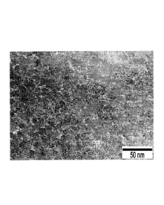
Figure 9 is a planar TEM image obtained in the evaluation of Example 4.
Figure 10 is a cross-sectional planar fEM image obtained in the evaluation of
Comparative Example 1. Figure 11 is a planar TEM image obtained for
Comparative
Example 1.
28
CA 02889741 2015-04-27
Figure 12 is an enlarged view of the planar [EM image shown in Figure 11
with some of the grains in a frame.
A comparison of the drawings clearly reveals that the vapor-deposited films
fabricated in Comparative Example was less uniform than the vapor-deposited
films
fabricated in Examples.
[0065] [Specific embodiments relating to determining manufacturing conditions]
1. Determining candidate vapor deposition conditions
Using ZrO2 as a vapor deposition source, ZrO2 vapor-deposited films were
formed to film thicknesses of about 70 mu by an ion-assisted method under
varying
ion-assisted conditions (condition 1, condition 2) on glass substrates. The
current and =
voltage of the ion gun were set higher in condition 2 than in condition 1.
[0066] 2. Evaluation of uniformity of TEM image
For each of the ZrO2 vapor-deposited films fabricated by vapor deposition
under condition 1 in 1. above and the ZrO2 vapor-deposited films fabricated by
vapor
deposition under condition 2, a piece of dummy glass was adhered with an
adhesive to
the ZrO2 vapor-deposited film from above and a sample was cut in the sectional
direction of the ZrO2 vapor-deposited film. Etching by ion milling was used to
shave
down the ZrO2 vapor-deposited film in the sectional direction. The etching was
stopped
when the thickness of the ZrO2 vapor-deposited film reached about 100 nm. The
sample
thus fabricated was placed in a transmission electron microscope and a cross-
sectional
image (bright-field image) was obtained at a magnification of 150,000-fold.
For each cross-sectional TEM image, commercial analysis software was used
to binary process the shade of a region 130 nm x 130 nm in area and the area
fractions
of the dark portions and bright portions were obtained. As a result, the value
of the ZrO2
29
CA 02889741 2015-04-27
vapor-deposited film fabricated by vapor deposition under condition 2 was
greater than
the value of the ZrO2 vapor-deposited film fabricated by vapor deposition
under
condition 1.
The absence or presence of the region the major axis length of which as an
actual size was equal to or more than 1 nm was determined in an area measuring
130
nm x 130 nm. As a result, the cross-sectional TEM image of the ZrO2 vapor-
deposited
film fabricated by vapor deposition under condition 2 was determined not to
have such
a region.
By contrast, columnar structures with a major axis length of equal to or more
than 1 nm as an actual size were found in the cross-sectional TEM image of the
ZrO2
vapor-deposited film fabricated by vapor deposition under condition 1. In the
ZrO2
vapor-deposited film fabricated by vapor deposition under condition 1,
multiple
columnar structures with major axis lengths of 2 nm to 40 nm and minor axis
lengths of
0.5 nm to 2 nm as an actual size were observed.
[0067] 3. Evaluation of heat resistance
A ZrO2 vapor-deposited film formed on a plastic lens substrate (product name
Eyas, made by 140YA Corp., refractive index 1.6, colorless lens) by the same
method as
in 1. above was placed for two hours in a heating furnace at the internal
furnace
temperature shown in Table 4, after which the presence of cracks several cm or
more in
length in the ZrO2 vapor-deposited film was evaluated under a fluorescent
lamp. The
presence of cracks was denoted by X and the absence of cracks was denoted by
0. The
results are given in Table 2.
CA 02889741 2015-04-27
[0068] [Table 2]
Internal temperature of Presence of cracks in ZrO2 Presence of cracks in
ZrO2
heating furnace vapor-deposited film vapor-deposited film
formed under condition 1 formed under
condition 2
80 C x 0
85 C x 0
90 C x 0
95 C
100 C x 0
[0069] Based on the above results, it was determined that the greater the
uniformity of
the cross-sectional LEM image, the better the heat resistance of the vapor-
deposited
film.
[0070] 4. Measurement of film stress
By the same method as set forth above, ZrO2 vapor-deposited films were
formed on the surface of cover glasses under condition identical to conditions
1 and 2.
When the film stress was measured, tensile stress was present under condition
1 and
compressive stress under condition 2.
[0071] 5. Evaluation of scratch resistance
A water-repellent film in the form of a fluorine-substituted alkyl
group-comprising organic silicon compound made by Shin-Etsu Chemical Co.,
Ltd.,
KY130, was vapor deposited by halogen heating on a ZrO2 vapor-deposited film
formed
on a plastic lens substrate (product name Eyas, made by HOYA Corp., refractive
index
1.6, colorless lens) by the same method as in 1. above and samples were
prepared.
31
CA 02889741 2015-04-27
The samples thus prepared were subjected to a scratch resistance test by
running steel wool back and forth 20 times with a load of 1 kg, and a scratch
resistance
test by running a sand eraser back and forth 5 times with a load of 3 kg.
Following the
scratch tests, the ZrO2 vapor-deposited film was observed under a fluorescent
lamp and
the presence or absence of scratches and cracks 5 mm or greater in length was
determined. For six or more scratches or cracks, the scratch resistance was
evaluated as
X, five or fewer but equal to or more than 2 as A, and one or none as 0.
[0072] 6. Measurement of film hardness (indentation hardness)
ZrO2 vapor-deposited films were formed on plastic lens substrates (product
name Eyas, made by HOYA Corp., refractive index 1.6, colorless lens) under
conditions
1 and 2 by the same method as in 1. above.
The indentation hardness of the ZrO2 vapor-deposited film that was formed
was measured by the following method with a measuring apparatus (Elionix ultra-
micro
indentation hardness tester ENT-2100).
In measurement, a triangular pyramid diamond indenter with an edge interval
of 115 degrees was employed. Measurement conditions were set in the form of an
indenter load rate of 0.2 mgf/sec, a maximum load of 0.98 mN maintained for 1
sec,
followed by unloading at the same load rate. The indentation depth at maximum
load
was read from an indenter indentation depth ¨ load curve obtained by this
measurement.
The indentation hardness H was calculated from the following equation.
1-1.---Pma,JA(hA) .. (1)
In the above equation, Pm ax denotes the maximum load, A(hA) denotes the
projected contact area of the indenter. A (hA) was obtained by first obtaining
hA from the
maximum indentation depth hm,õ and the intersection h, of the unloading curve
gradient
32
CA 02889741 2015-04-27
and the displacement axis, and then from the geometric shape (vertical angle
65.03 ) of
the regular triangular pyramide (Berkovich type) indenter comprised of
diamond. The
equations for hA and A (hA) are both given below:
hA=4õaõ-0.75(hr,,,õ-hs) .. (2)
A(hA)=3r3tan2(65.03 )hA2- - = (3)
(In this context, 0.75 in equation (2) is a constant of a Berkovieh type
indenter.)
[0073] In the measurement results, the indentation hardness of the ZrO2
vapor-deposited film formed under condition 2 achieved a higher value than the
indentation hardness of the ZrO2 vapor-deposited film formed under condition
1.
[0074] The above results are given in Table 3.
[0075] [Table 3]
Presence of cracks in Presence of cracks in
ZrO2 vapor-deposited film ZrO2 vapor-deposited
formed under condition 1 film formed under
condition 2
Scratch resistance test by
running steel wool back and
forth 20 times at a load of 1 kg
Scratch resistance test by
running sand eraser back and
forth 5 times at a load of 3 kg
Indentation hardness low high
[0076] From the above results, it was determined that the higher the
uniformity of the
33
CA 02889741 2015-04-27
cross-sectional 1EM image, the better the scratch resistance of the vapor-
deposited film.
The fact that vapor deposition condition permitting the fabrication of vapor-
deposited
films with good scratch resistance can be determined by the simple method of
image
analysis without requiring stress or hardness measurement in this manner is
one of the
advantages afforded by an aspect of the present invention.
[0077] When the average grain size and the grain boundary occupancy rate
observed
in the planar TEM images were obtained by the methods set forth above for the
ZrO2
vapor-deposited film prepared under condition 1 and the ZrO2 vapor-deposited
film
prepared under condition 2, the ZrO2 vapor-deposited film prepared under
condition 2
exhibited an average grain size of equal to or greater than 3.5 ntn and a
grain boundary
occupancy rate of less than 15%. By contrast, the ZrO2 vapor-deposited film
prepared
under condition 1 exhibited a grain boundary occupancy rate exceeding 15% and
an
average grain size of less than 3.5 nm.
[0078] 7. Preparation of eyeglass lenses
A total of 8 layers of vapor-deposited films, shown in Table 4 below, were
sequentially formed by an ion-assisted method using an assist gas in the form
of oxygen
gas or a mixed gas of oxygen and argon on the surface of a hard coat on the
convex side
of a plastic lens substrate (product name Eyas, made by HOYA Corp., refractive
index
1.6, colorless lens) having a convex surface on the object side and a concave
surface on
the eyeball side, with both sides having been optically finished and coated
with hard
coats in advance. After forming the 8th vapor-deposited film, a 9th layer film
in the
form of a water-repellent layer was formed over it by vapor deposition by
halogen
heating using a vapor deposition source in the form of KY130, which is a
fluorine-substituted alkyl group-comprising organic silicon compound made by
34
CA 02889741 2015-04-27
=
Shin-Etsu Chemical Co., Ltd. Two types (eyeglass lenses 1 and 2) were
prepared.
During the fabrication of eyeglass lens 1, above condition 1 was employed as
the vapor
deposition condition of the ZrO2 vapor-deposited film. During the fabrication
of
eyeglass lens 2, above condition 2 was employed as the vapor deposition
condition of
the ZrO2 vapor-deposited film. The other manufacturing conditions were
identical.
[0079] [Table 4]
Vapor deposition source Film thickness
(urn)
1st layer SiO2 30
2"d layer ZrO2 10
3rd layer SiO2 200
4th layer ITO 10
5th layer ZrO2 30
6t11 layer SiO2 20
7th layer ZrO2 60
8th layer SiO2 90
[0080] 8. Heat resistance test of eyeglass lens samples
The eyeglass lenses fabricated in 7. above were placed for 1 hour in a 100 C
oven, held up to a fluorescent lamp, and visually evaluated for the presence
of cracks.
As a result, the eyeglass lens 1 that had been fabricated with the ZrO2 vapor-
deposited
film under condition 1 exhibited many cracks running several cm in length in
the ZrO2
vapor-deposited film, but the eyeglass lens 2 that had been fabricated with
the ZrO2
vapor-deposited film under condition 2 afforded a high degree of transparence
and did
not exhibit cracks.
[0081] 9. Scratch resistance test of eyeglass lens samples
The eyeglass lenses fabricated in 7. above were subjected to a scratch
CA 02889741 2015-04-27
resistance test by running steel wool back and forth 20 times with a load of 1
kg, and a
scratch resistance test by running a sand eraser back and forth 5 times with a
load of 3
kg. As a result, the eyeglass lens that had been fabricated with the ZrO2
vapor-deposited
film under condition 1 exhibited several scratches and cracks, but the
eyeglass lens
fabricated with the ZrO2 vapor-deposited film under condition 2 afforded a
high degree
of transparence and did not develop scratches or cracks.
[0082] Based on the results of 8. and 9., the fabrication of ZrO2 vapor-
deposited films
under vapor deposition conditions determined to be good for heat resistance
and scratch
resistance based on the uniformity of the TEM image was confirmed to yield
eyeglass
lenses having good durability and scratch resistance. Conventionally, the
discovery of
vapor deposition conditions permitting the forming of vapor-deposited films
with good
heat resistance and scratch resistance would require repeatedly implementing
an
accelerated durability test such as the oven heating implemented in 8. above,
implementing the scratch resistance tests on eyeglass lens samples that was
implemented in 9 above, and selecting candidate conditions. By contrast, an
aspect of
the invention makes it possible to determine manufacturing conditions
permitting the
manufacturing of eyeglass lenses having good durability by the simple method
of
fabricating test vapor-deposited films as well as obtaining the TEM images
thereof and
evaluating the imiformity.
INDUSTRIAL APPLICABILITY
[0083] The present invention is useful in the field of manufacturing eyeglass
lenses.
36