Note: Descriptions are shown in the official language in which they were submitted.
CA 03051255 2019-07-22
WO 2018/144939
PCT/US2018/016733
INDEPENDENT BAND DETECTION FOR
NETWORK PROTECTION
BACKGROUND
[0001] Signal boosters and repeaters can be used to increase the quality of
wireless
communication between a wireless device and a wireless communication access
point,
such as a cell tower. Signal boosters can improve the quality of the wireless
communication by amplifying, filtering, and/or applying other processing
techniques to
uplink and downlink signals communicated between the wireless device and the
wireless
communication access point.
[0002] As an example, the signal booster can receive, via an antenna, downlink
signals
from the wireless communication access point. The signal booster can amplify
the
downlink signal and then provide an amplified downlink signal to the wireless
device. In
other words, the signal booster can act as a relay between the wireless device
and the
wireless communication access point. As a result, the wireless device can
receive a
stronger signal from the wireless communication access point. Similarly,
uplink signals
from the wireless device (e.g., telephone calls and other data) can be
directed to the signal
booster. The signal booster can amplify the uplink signals before
communicating, via an
antenna, the uplink signals to the wireless communication access point.
BRIEF DESCRIPTION OF THE DRAWINGS
[0003] Features and advantages of the disclosure will be apparent from the
detailed
description which follows, taken in conjunction with the accompanying
drawings, which
together illustrate, by way of example, features of the disclosure; and,
wherein:
[0004] FIG. 1 illustrates a signal booster in communication with a wireless
device and a
base station in accordance with an example;
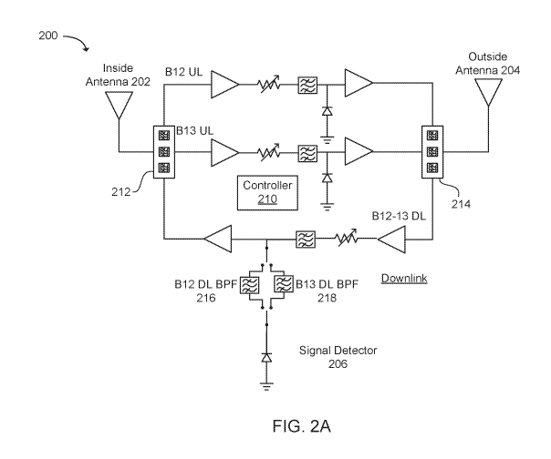
[0005] FIG. 2A illustrates a signal booster operable to independently control
uplink gains
or noise powers for multiple bands in uplink signal paths based on control
information
detected from a downlink signal path that combines multiple bands in
accordance with an
example;
1
CA 03051255 2019-07-22
WO 2018/144939
PCT/US2018/016733
[0006] FIG. 2B illustrates a signal booster in accordance with an example;
[0007] FIG. 2C illustrates a signal booster in accordance with an example;
[0008] FIGS. 3 to 5 illustrate a signal booster in accordance with an example;
and
[0009] FIG 6 illustrates a wireless device in accordance with an example.
[0010] Reference will now be made to the exemplary embodiments illustrated,
and
specific language will be used herein to describe the same. It will
nevertheless be
understood that no limitation of the scope of the invention is thereby
intended.
DETAILED DESCRIPTION
[0011] Before the present invention is disclosed and described, it is to be
understood that
this invention is not limited to the particular structures, process steps, or
materials
disclosed herein, but is extended to equivalents thereof as would be
recognized by those
ordinarily skilled in the relevant arts. It should also be understood that
terminology
employed herein is used for the purpose of describing particular examples only
and is not
intended to be limiting. The same reference numerals in different drawings
represent the
same element. Numbers provided in flow charts and processes are provided for
clarity in
illustrating steps and operations and do not necessarily indicate a particular
order or
sequence.
EXAMPLE EMBODIMENTS
[0012] An initial overview of technology embodiments is provided below and
then
specific technology embodiments are described in further detail later. This
initial
summary is intended to aid readers in understanding the technology more
quickly but is
not intended to identify key features or essential features of the technology
nor is it
intended to limit the scope of the claimed subject matter.
[0013] FIG. 1 illustrates an exemplary signal booster 120 in communication
with a
wireless device 110 and a base station 130. The signal booster 120 can be
referred to as a
repeater. A repeater can be an electronic device used to amplify (or boost)
signals. The
signal booster 120 (also referred to as a cellular signal amplifier) can
improve the quality
of wireless communication by amplifying, filtering, and/or applying other
processing
2
CA 03051255 2019-07-22
WO 2018/144939
PCT/US2018/016733
techniques via a signal amplifier 122 to uplink signals communicated from the
wireless
device 110 to the base station 130 and/or downlink signals communicated from
the base
station 130 to the wireless device 110. In other words, the signal booster 120
can amplify
or boost uplink signals and/or downlink signals bi-directionally. In one
example, the
signal booster 120 can be at a fixed location, such as in a home or office.
Alternatively,
the signal booster 120 can be attached to a mobile object, such as a vehicle
or a wireless
device 110.
[0014] In one configuration, the signal booster 120 can include an integrated
device
antenna 124 (e.g., an inside antenna or a coupling antenna) and an integrated
node
antenna 126 (e.g., an outside antenna). The integrated node antenna 126 can
receive the
downlink signal from the base station 130. The downlink signal can be provided
to the
signal amplifier 122 via a second coaxial cable 127 or other type of radio
frequency
connection operable to communicate radio frequency signals. The signal
amplifier 122
can include one or more cellular signal amplifiers for amplification and
filtering. The
downlink signal that has been amplified and filtered can be provided to the
integrated
device antenna 124 via a first coaxial cable 125 or other type of radio
frequency
connection operable to communicate radio frequency signals. The integrated
device
antenna 124 can wirelessly communicate the downlink signal that has been
amplified and
filtered to the wireless device 110.
[0015] Similarly, the integrated device antenna 124 can receive an uplink
signal from the
wireless device 110. The uplink signal can be provided to the signal amplifier
122 via the
first coaxial cable 125 or other type of radio frequency connection operable
to
communicate radio frequency signals. The signal amplifier 122 can include one
or more
cellular signal amplifiers for amplification and filtering. The uplink signal
that has been
amplified and filtered can be provided to the integrated node antenna 126 via
the second
coaxial cable 127 or other type of radio frequency connection operable to
communicate
radio frequency signals. The integrated device antenna 126 can communicate the
uplink
signal that has been amplified and filtered to the base station 130.
[0016] In one example, the signal booster 120 can filter the uplink and
downlink signals
.. using any suitable analog or digital filtering technology including, but
not limited to,
surface acoustic wave (SAW) filters, bulk acoustic wave (BAW) filters, film
bulk acoustic
3
CA 03051255 2019-07-22
WO 2018/144939
PCT/US2018/016733
resonator (FBAR) filters, ceramic filters, waveguide filters or low-
temperature co-fired
ceramic (LTCC) filters.
[0017] In one example, the signal booster 120 can send uplink signals to a
node and/or
receive downlink signals from the node. The node can comprise a wireless wide
area
network (WWAN) access point (AP), a base station (BS), an evolved Node B
(eNB), a
baseband unit (BBU), a remote radio head (RRH), a remote radio equipment
(RRE), a
relay station (RS), a radio equipment (RE), a remote radio unit (RRU), a
central
processing module (CPM), or another type of WWAN access point.
[0018] In one configuration, the signal booster 120 used to amplify the uplink
and/or a
downlink signal is a handheld booster. The handheld booster can be implemented
in a
sleeve of the wireless device 110. The wireless device sleeve can be attached
to the
wireless device 110, but can be removed as needed. In this configuration, the
signal
booster 120 can automatically power down or cease amplification when the
wireless
device 110 approaches a particular base station. In other words, the signal
booster 120 can
determine to stop performing signal amplification when the quality of uplink
and/or
downlink signals is above a defined threshold based on a location of the
wireless device
110 in relation to the base station 130.
[0019] In one example, the signal booster 120 can include a battery to provide
power to
various components, such as the signal amplifier 122, the integrated device
antenna 124
and the integrated node antenna 126. The battery can also power the wireless
device 110
(e.g., phone or tablet). Alternatively, the signal booster 120 can receive
power from the
wireless device 110.
[0020] In one configuration, the signal booster 120 can be a Federal
Communications
Commission (FCC)-compatible consumer signal booster. As a non-limiting
example, the
signal booster 120 can be compatible with FCC Part 20 or 47 Code of Federal
Regulations (C.F.R.) Part 20.21 (March 21, 2013). In addition, the signal
booster 120 can
operate on the frequencies used for the provision of subscriber-based services
under parts
22 (Cellular), 24 (Broadband PCS), 27 (AWS-1, 700 MHz Lower A-E Blocks, and
700
MHz Upper C Block), and 90 (Specialized Mobile Radio) of 47 C.F.R. The signal
booster
120 can be configured to automatically self-monitor its operation to ensure
compliance
with applicable noise and gain limits. The signal booster 120 can either self-
correct or
4
CA 03051255 2019-07-22
WO 2018/144939
PCT/US2018/016733
shut down automatically if the signal booster's operations violate the
regulations defined
in FCC Part 20.21.
[0021] In one configuration, the signal booster 120 can improve the wireless
connection
between the wireless device 110 and the base station 130 (e.g., cell tower) or
another type
of wireless wide area network (WWAN) access point (AP). The signal booster 120
can
boost signals for cellular standards, such as the Third Generation Partnership
Project
(3GPP) Long Term Evolution (LTE) Release 8, 9, 10, 11, 12, or 13 standards or
Institute
of Electronics and Electrical Engineers (IEEE) 802.16. In one configuration,
the signal
booster 120 can boost signals for 3GPP LTE Release 13Ø0 (March 2016) or
other
desired releases. The signal booster 120 can boost signals from the 3GPP
Technical
Specification 36.101 (Release 12 Jun 2015) bands or LTE frequency bands. For
example,
the signal booster 120 can boost signals from the LTE frequency bands: 2, 4,
5, 12, 13,
17, and 25. In addition, the signal booster 120 can boost selected frequency
bands based
on the country or region in which the signal booster is used, including any of
bands 1-70
or other bands, as disclosed in ETSI T5136 104 V13.5.0 (2016-10).
[0022] The number of LTE frequency bands and the level of signal improvement
can vary
based on a particular wireless device, cellular node, or location. Additional
domestic and
international frequencies can also be included to offer increased
functionality. Selected
models of the signal booster 120 can be configured to operate with selected
frequency
bands based on the location of use. In another example, the signal booster 120
can
automatically sense from the wireless device 110 or base station 130 (or GPS,
etc.) which
frequencies are used, which can be a benefit for international travelers.
[0023] In one example, the integrated device antenna 124 and the integrated
node antenna
126 can be comprised of a single antenna, an antenna array, or have a
telescoping form-
factor. In another example, the integrated device antenna 124 and the
integrated node
antenna 126 can be a microchip antenna. An example of a microchip antenna is
AMMAL001. In yet another example, the integrated device antenna 124 and the
integrated node antenna 126 can be a printed circuit board (PCB) antenna. An
example of
a PCB antenna is TE 2118310-1.
.. [0024] In one example, the integrated device antenna 124 can receive uplink
(UL) signals
from the wireless device 110 and transmit DL signals to the wireless device
110 using a
5
CA 03051255 2019-07-22
WO 2018/144939
PCT/US2018/016733
single antenna. Alternatively, the integrated device antenna 124 can receive
UL signals
from the wireless device 110 using a dedicated UL antenna, and the integrated
device
antenna 124 can transmit DL signals to the wireless device 110 using a
dedicated DL
antenna.
[0025] In one example, the integrated device antenna 124 can communicate with
the
wireless device 110 using near field communication. Alternatively, the
integrated device
antenna 124 can communicate with the wireless device 110 using far field
communication.
[0026] In one example, the integrated node antenna 126 can receive downlink
(DL)
signals from the base station 130 and transmit uplink (UL) signals to the base
station 130
via a single antenna. Alternatively, the integrated node antenna 126 can
receive DL
signals from the base station 130 using a dedicated DL antenna, and the
integrated node
antenna 126 can transmit UL signals to the base station 130 using a dedicated
UL
antenna.
[0027] In one configuration, multiple signal boosters can be used to amplify
UL and DL
signals. For example, a first signal booster can be used to amplify UL signals
and a
second signal booster can be used to amplify DL signals. In addition,
different signal
boosters can be used to amplify different frequency ranges.
[0028] In one configuration, the signal booster 120 can be configured to
identify when
the wireless device 110 receives a relatively strong downlink signal. An
example of a
strong downlink signal can be a downlink signal with a signal strength greater
than
approximately -80dBm. The signal booster 120 can be configured to
automatically turn
off selected features, such as amplification, to conserve battery life. When
the signal
booster 120 senses that the wireless device 110 is receiving a relatively weak
downlink
signal, the integrated booster can be configured to provide amplification of
the downlink
signal. An example of a weak downlink signal can be a downlink signal with a
signal
strength less than -80dBm.
[0029] In one example, the signal booster 120 can also include one or more of:
a
waterproof casing, a shock absorbent casing, a flip-cover, a wallet, or extra
memory
storage for the wireless device. In one example, extra memory storage can be
achieved
with a direct connection between the signal booster 120 and the wireless
device 110. In
6
CA 03051255 2019-07-22
WO 2018/144939
PCT/US2018/016733
another example, Near-Field Communications (NFC), Bluetooth v4.0, Bluetooth
Low
Energy, Bluetooth v4.1, Bluetooth v4.2, Bluetooth 5, Ultra High Frequency
(UHF), 3GPP
LTE, Institute of Electronics and Electrical Engineers (IEEE) 802.11a, IEEE
802.11b,
IEEE 802.11g, IEEE 802.11n, IEEE 802.11ac, or IEEE 802.11ad can be used to
couple
the signal booster 120 with the wireless device 110 to enable data from the
wireless
device 110 to be communicated to and stored in the extra memory storage that
is
integrated in the signal booster 120. Alternatively, a connector can be used
to connect the
wireless device 110 to the extra memory storage.
[0030] In one example, the signal booster 120 can include photovoltaic cells
or solar
panels as a technique of charging the integrated battery and/or a battery of
the wireless
device 110. In another example, the signal booster 120 can be configured to
communicate
directly with other wireless devices with signal boosters. In one example, the
integrated
node antenna 126 can communicate over Very High Frequency (VHF) communications
directly with integrated node antennas of other signal boosters. The signal
booster 120
can be configured to communicate with the wireless device 110 through a direct
connection, Near-Field Communications (NFC), Bluetooth v4.0, Bluetooth Low
Energy,
Bluetooth v4.1, Bluetooth v4.2, Ultra High Frequency (UHF), 3GPP LTE,
Institute of
Electronics and Electrical Engineers (IEEE) 802.11a, IEEE 802.11b, IEEE
802.11g, IEEE
802.11n, IEEE 802.11ac, IEEE 802.11ad, a TV White Space Band (TVWS), or any
other
industrial, scientific and medical (ISM) radio band. Examples of such ISM
bands include
2.4 GHz, 3.6 GHz, 4.9 GHz, 5 GHz, or 5.9 GHz. This configuration can allow
data to
pass at high rates between multiple wireless devices with signal boosters.
This
configuration can also allow users to send text messages, initiate phone
calls, and engage
in video communications between wireless devices with signal boosters. In one
example,
the integrated node antenna 126 can be configured to couple to the wireless
device 110. In
other words, communications between the integrated node antenna 126 and the
wireless
device 110 can bypass the integrated booster.
[0031] In another example, a separate VHF node antenna can be configured to
communicate over VHF communications directly with separate VHF node antennas
of
other signal boosters. This configuration can allow the integrated node
antenna 126 to be
used for simultaneous cellular communications. The separate VHF node antenna
can be
configured to communicate with the wireless device 110 through a direct
connection,
7
CA 03051255 2019-07-22
WO 2018/144939
PCT/US2018/016733
Near-Field Communications (NFC), Bluetooth v4.0, Bluetooth Low Energy,
Bluetooth
v4.1, Bluetooth v4.2, Ultra High Frequency (UHF), 3GPP LTE, Institute of
Electronics
and Electrical Engineers (IEEE) 802.11a, IEEE 802.11b, IEEE 802.11g, IEEE
802.11n,
IEEE 802.11ac, IEEE 802.11ad, a TV White Space Band (TVWS), or any other
industrial,
scientific and medical (ISM) radio band.
[0032] In one configuration, the signal booster 120 can be configured for
satellite
communication. In one example, the integrated node antenna 126 can be
configured to act
as a satellite communication antenna. In another example, a separate node
antenna can be
used for satellite communications. The signal booster 120 can extend the range
of
coverage of the wireless device 110 configured for satellite communication.
The
integrated node antenna 126 can receive downlink signals from satellite
communications
for the wireless device 110. The signal booster 120 can filter and amplify the
downlink
signals from the satellite communication. In another example, during satellite
communications, the wireless device 110 can be configured to couple to the
signal
booster 120 via a direct connection or an ISM radio band. Examples of such ISM
bands
include 2.4 GHz, 3.6 GHz, 4.9 GHz, 5 GHz, or 5.9 GHz.
[0033] FIG. 2A illustrates an exemplary signal booster 200. The signal booster
200 can
include one or more uplink signal paths for selected bands, and the signal
booster 200 can
include one or more downlink signal paths for selected bands. The uplink
signal paths can
include one or more amplifiers and band pass filters to amplify uplink
signals. Similarly,
the downlink signal paths can include one or more amplifiers and band pass
filters to
amplify downlink signals.
[0034] In the example shown in FIG. 2A, the signal booster 200 can have a
first uplink
signal path for band 12 (B12) and a second uplink signal path for B13. In
uplink, B12
corresponds to a frequency range of 699 megahertz (MHz) to 716 MHz, and B13
corresponds to a frequency range of 777 MHz to 787 MHz. In addition, in this
example,
the signal booster 200 can have a downlink signal path for both B12 and B13.
In other
words, the downlink signal path can be a combined downlink signal path for
both B12
and B13. In downlink, B12 corresponds to a frequency range of 729 MHz to 746
MHz,
and B13 corresponds to a frequency range of 746 MHz to 756 MHz. In the
downlink, B12
and B13 are spectrally adjacent to each other.
8
CA 03051255 2019-07-22
WO 2018/144939
PCT/US2018/016733
[0035] In one example, the signal booster 200 can receive uplink signals from
a mobile
device (not shown) via an inside antenna 202 coupled to the signal booster
200. An uplink
signal can pass through a first multiband filter 212, and then the uplink
signal can be
provided to the first uplink signal path for B12 or the second uplink signal
path for B13.
The first and second uplink signal paths can perform amplification and
filtering of the
uplink signal. The uplink signal can be provided to a second multiband filter
214, and
then the uplink signal can be provided to a base station (not shown) via an
outside
antenna 204 coupled to the signal booster 200.
[0036] In another example, the signal booster 200 can receive downlink signals
from the
base station via the outside antenna 204. A downlink signal can pass through
the second
multiband filter 214, and then the downlink signal can be provided to the
combined
downlink signal path for both B12 and B13. The combined downlink signal path
can
perform amplification and filtering of the downlink signal. The downlink
signal can be
provided to the first multiband filter 212, and then the downlink signal can
be provided to
the mobile device via the inside antenna 202.
[0037] In one configuration, the signal booster 200 can include a controller
210.
Generally speaking, the controller 210 can be configured to perform network
protection
for the signal booster 200. The controller 210 can perform network protection
in
accordance with Part 20 of the Federal Communications Commission (FCC)
Consumer
Booster Rules. The FCC Consumer Booster Rules necessitate that uplink signal
paths and
downlink signal are to work together for network protection. Network
protection can be
performed in order to protect a cellular network from overload or noise floor
increase.
The controller 210 can perform network protection by adjusting a gain or noise
power for
each band in the uplink transmission paths based on control information from
each band
in the downlink transmission paths. The control information from each band in
the
downlink transmission paths can include a received signal strength indication
(RSSI)
associated with downlink received signals. In other words, based on the RSSI
of the
downlink received signals traveling on the downlink transmission paths, the
controller
210 can adjust (i.e., increase or decrease) the gain or noise power for the
uplink
transmission paths. By adjusting the gain or noise floor when performing the
network
protection, the signal booster 200 can prevent the network (e.g., base
stations) from
becoming overloaded with uplink signals from the signal booster 200 that
exceed a
9
CA 03051255 2019-07-22
WO 2018/144939
PCT/US2018/016733
defined threshold.
[0038] In traditional signal boosters, uplink signal paths can be separate for
B12 and B13,
while a combined downlink signal path can exist for B12 and B13. In other
words, all the
power from B12 and B13 in downlink can move through the combined downlink
signal
path. Since B12 and B13 are combined in the downlink, in traditional signal
boosters, the
network is protected based on an extra strong downlink signal since the uplink
gain or
noise floor is adjusted based on the combined power of downlink received
signals for B12
and B13. In traditional signal boosters, the uplink gain or noise floor for
B12 can be
adjusted based on the combined power of downlink received signals for B12 and
B13,
and similarly, the uplink gain or noise floor for B13 can be adjusted based on
the
combined power of downlink received signals for B12 and B13. As a result, the
adjustment to the uplink gain or noise floor for B12 and B13 may not actually
be
reflective of the power associated with the downlink received signals.
[0039] In the example shown in FIG. 2A, the controller 210 can separately
detect the
control information (e.g., RSSI) for downlink received signals with respect to
B12 and
B13. In other words, the signal booster 200 can detect control information
that pertains
only to downlink received signals for B12. Similarly, the signal booster 200
can detect
control information that pertains only to downlink received signals for B13.
The
controller 210 can adjust the uplink gain or noise floor for B12 based only on
the control
information for the downlink received signals on B12. Similarly, the
controller 210 can
adjust the uplink gain or noise floor for B13 based only on the control
information for the
downlink received signals on B13. In other words, the uplink gain or noise
power for B12
can be controlled independent of the uplink gain or noise power for B13.
[0040] More specifically, as shown in FIG 2A, the signal booster 200 can
include a
switchable B12 downlink band pass filter 216, a switchable B13 downlink
bandpass filter
218, and a signal detector 206. The switchable B12 downlink bandpass filter
216 and the
switchable B13 downlink bandpass filter 218 can be switched in and out, such
that
downlink received signals for B12 can be provided to the signal detector 206
or downlink
received signals for B13 can be provided to the signal detector 206. The
signal detector
206 can be a log detector (e.g., a diode), and the signal detector 206 can
detect the control
information (e.g., RSSI) associated with the downlink received signals for B12
or the
CA 03051255 2019-07-22
WO 2018/144939
PCT/US2018/016733
downlink received signals for B13. In other words, the switchable B12 downlink
band
pass filter 216 and the switchable B13 downlink bandpass filter 218 can enable
the signal
detector 206 to separately detect the control information for downlink
received signals for
B12 and B13. The signal detector 206 can provide the control information to
the
controller 210. Based only on the control information for downlink received
signals for
B12, the controller 210 can adjust the uplink gain or noise floor for B12.
Similarly, based
only on the control information for downlink received signals for B13, the
controller 210
can adjust the uplink gain or noise floor for B13.
[0041] In general, using the signal detector 206, the controller 210 can
detect single
downlink bands while multiple downlink bands are passing through a common
downlink
signal path. With respect to the specific example shown in FIG 2A, the
controller 210 can
perform independent detection of control information for B12 and B13, even
though the
signal booster 200 has a combined downlink signal path for B12 and B13.
[0042] In an alternative configuration, the signal booster 200 can include a
first signal
detector and a second signal detector. The first signal detector can detect
control
information (e.g., RSSI) associated with a received downlink signal for B12.
The second
signal detector can detect control information (e.g., RSSI) associated with a
received
downlink signal for B13. Therefore, in this configuration, separate signal
detectors can be
utilized to detect the control information for the multiple bands.
[0043] FIG 2B illustrates an exemplary signal booster 200. The signal booster
200 can
include one or more uplink signal paths for selected bands, and the signal
booster 200 can
include one or more downlink signal paths for selected bands. The uplink
signal paths can
include one or more amplifiers and band pass filters to amplify uplink
signals. Similarly,
the downlink signal paths can include one or more amplifiers and band pass
filters to
amplify downlink signals. In addition, the signal booster 200 can include a
controller 210
that is configured to perform network protection for the signal booster 200.
[0044] In one configuration, a downlink signal path can include a signal
detector 220.
The signal detector 220 can be positioned after an amplifier in the downlink
signal path,
but prior to switchable B12 or B13 downlink band pass filters 216, 218 in the
downlink
signal path. The signal detector 220 can measure a power level of a downlink
signal that
is traveling on the downlink signal path. The power level of the signal can be
utilized to
11
CA 03051255 2019-07-22
WO 2018/144939
PCT/US2018/016733
perform automatic gain control (AGC) and to maintain linearity for downlink
signals.
[0045] In one configuration, the signal booster 200 can include a downlink
signal path
that directs a downlink signal in a first band to a switchable bandpass filter
associated
with a second band when a power level of the downlink signal is greater than a
defined
threshold. The switchable bandpass filter can cause a reduction in the power
level of the
downlink signal, which can avoid a performance of automatic gain control (AGC)
for the
first band. As an example, the signal booster 200 can include a downlink
signal path that
directs a downlink signal in B12 to a switchable bandpass filter 218
associated with B13
when a power level associated with the downlink signal in B12 is greater than
the defined
threshold. The switchable bandpass filter 218 associated with B13 can reduce
the power
level of the downlink signal, and as a result, the signal booster 200 may not
perform AGC
for B12.
[0046] FIG 2C illustrates an exemplary signal booster 200. The signal booster
200 can
include one or more uplink signal paths for selected bands, and the signal
booster 200 can
include one or more downlink signal paths for selected bands. The uplink
signal paths can
include one or more amplifiers and band pass filters to amplify uplink
signals. Similarly,
the downlink signal paths can include one or more amplifiers and band pass
filters to
amplify downlink signals. In addition, the signal booster 200 can include a
controller 210
that is configured to perform network protection for the signal booster 200.
[0047] In one configuration, a downlink signal path can include a signal
detector 206.
More specifically, the downlink signal path can include a pass through signal
path 222 to
the signal detector 206. The pass through signal path 222 can bypass
switchable B12 and
B13 downlink band pass filters 216, 218 in the downlink signal path. The
signal detector
206 can measure a signal power level for the pass through signal path 222. The
signal
power level can be utilized to perform automatic gain control (AGC) and to
maintain
linearity for downlink signals.
[0048] In one example, a downlink signal for B12 can be directed to the signal
detector
206 via the switchable B12 bandpass filter 216. The signal detector 206 can
measure a
power level of the downlink signal for B12. Depending on the power level in
relation to a
defined threshold, the controller 210 can perform network protection for an
uplink signal
path for B12. In another example, a downlink signal for B13 can be directed to
the signal
12
CA 03051255 2019-07-22
WO 2018/144939
PCT/US2018/016733
detector 206 via the switchable B13 bandpass filter 218. The signal detector
206 can
measure a power level of the downlink signal for B13. Depending on the power
level in
relation to a defined threshold, the controller 210 can perform network
protection for an
uplink signal path for B13. In some cases, the downlink signal for B12 or B13
may not be
.. directed to the switchable B12 bandpass filter 216 or the switchable B13
bandpass filter
218. Rather, the downlink signal can be provided directly to the signal
detector 206 via
the pass through signal path 222.
[0049] In one configuration, a signal booster (or repeater) can employ a
single-input
single-output (SISO) and/or double-input single-output (DISO) filtering
architecture,
.. which can allow multiple bands to share a same radio frequency (RF) path
(e.g., B12 and
B13 can share a same uplink path, or B12 and B13 can share a same downlink
path),
thereby reducing the number of components and the cost of the signal booster.
However,
when multiple bands share the same RF path, the performance of the signal
booster can
degrade. This reduction in performance can occur because every band sharing
the same
RF path is automatic gain controlled at a lowest automatic gain control (AGC)
value
between the multiple bands. In other words, the multiple bands on the same RF
path can
all use a lowest AGC value between the multiple bands. A band that is
automatic gain
controlled before its actual or true AGC value is reached can output less
power as
compared to a maximum potential for that band.
[0050] In one configuration, varying architectures can be employed in signal
boosters to
enable band/frequency-specific detection from a shared signal chain. In a
first
architecture, a diplexer can be used to separate bands in the signal booster.
For example, a
diplexer can be used to separate band 5 (B5) from B12 and B13. The diplexer
can be
positioned before a detector in the signal booster. In this architecture, a
detector
sensitivity can be adjusted for B5 separately from B12 and B13. In this
example, B12 and
B13 can be automatic gain controlled at different values as compared to an AGC
value for
B5. This architecture can be employed for any combination of bands sharing the
same RF
path, with correct filtering before the detector, and variations of pickup
resistor values in
series with those filters. In a second architecture, an RF switch can be
employed in the
signal booster. The RF switch can allow switching between RF paths containing
bandpass
filters for each band sharing the RF path.
13
CA 03051255 2019-07-22
WO 2018/144939
PCT/US2018/016733
[0051] In a third architecture, as described in further detail below, rather
than using an RF
switch, the signal booster can include multiple tap points off of the signal
chain, which
can enable band/frequency-specific detection from the signal chain. This
architecture is
not limited to the SISO architecture implementation, and can be applicable to
any signal
chain that passes multiple frequencies. The elimination of the RF switch in
the third
architecture can decrease complexity and cost of the signal booster.
[0052] FIG. 3 illustrates an exemplary signal booster 300 (or repeater). The
signal booster
300 can include a first multiband filter 312 and a second multiband filter
314. The first
multiband filter 312 can be communicatively coupled to an inside antenna 302,
and the
second multiband filter 314 can be communicatively coupled to an outside
antenna 304.
The signal booster 300 can include an uplink (UL) signal path communicatively
coupled
between the first multiband filter 312 and the second multiband filter 314.
The signal
booster 300 can include a downlink (DL) signal path communicatively coupled
between
the first multiband filter 312 and the second multiband filter 314. The UL
signal path can
include one or more amplifiers and filters. For example, the UL signal path
can include a
low noise amplifier (LNA), 316 a filter 318 (e.g., a SISO filter) and a power
amplifier
(PA) 326. Similarly, the DL signal path can include one or more amplifiers and
filters. For
example, the DL signal path can include a LNA 330, a filter 332 (e.g., a SISO
filter) and a
PA 334.
[0053] In one example, the UL signal path and/or the DL signal path can be
communicatively coupled to multiple tap paths. For example, as shown, the UL
signal
path can be communicatively coupled to a first tap path and a second tap path.
The first
tap path can include a first resistor (R1) 320 and the second tap path can
include a second
resistor (R2) 322. The first tap path and the second tap path can be
communicatively
coupled to a filter 324 (e.g., a DISO filter), and the filter 324 can be
communicatively
coupled to a signal detector 328. In one example, the DL signal path can be
communicatively coupled to a separate first tap path, a separate second tap
path, a
separate filter and a separate signal detector, similar to the UL signal path.
[0054] In one example, an uplink signal can be received at the inside antenna
302. The
uplink signal can travel to the first multiband filter 312, and the uplink
signal can be
directed to the uplink signal path. The uplink signal can pass through the LNA
316 and
14
CA 03051255 2019-07-22
WO 2018/144939
PCT/US2018/016733
the filter 318. Then, the uplink signal can be provided to the first tap path
and the second
tap path, and then through the filter 324. At this point, a power level of the
uplink signal
passing through the filter 324 can be detected at the signal detector 328.
[0055] In some cases, signals in one band of the uplink signal path can enter
the signal
detector 328 at a different level (e.g., a higher or lower power level) as
compared to
another band of the uplink signal path. For example, signals in B12 can enter
the signal
detector 328 at a higher decibel (dB) level as compared to signals in B13 that
enter the
signal detector 328, or vice versa.
[0056] Therefore, as shown in FIG 3, the first tap path and the second tap
path can
function to level out detected power level differences (or detection
variances) between the
different bands in the UL signal path. For example, a value of R1 320 and a
value of R2
322 can be physically adjusted, such that if one band is stronger than the
other band, the
value of R1 320 and the value of R2 322 can be adjusted to balance out the
power levels
between the two bands in the UL signal path. As an example, if signals in B12
are
stronger (i.e., have a higher dB value) as compared to signals in B13, the
value of R1 320
and the value of R2 322 can be adjusted higher or lower, respectively. The
signals can
pass through the filter 324, which can include a B12 filter and a B13 filter.
As a result,
both B12 and B13 can use a same AGC value. In other words, the value of R1 320
and
the value of R2 322 can be adjusted such that both B12 and B13 react to a same
AGC
value, even when signals in B12 are received at a higher power level as
compared to
signals in B13, or vice versa.
[0057] In the example shown in FIG. 3, the signal booster 300 may be unable to
perform
band/frequency-specific detection. For example, the signal booster 300 may be
unable to
distinguish signals in B12 from signals in B13. However, the value of R1 320
and the
value of R2 322 can be adjusted such that both B12 and B13 react to a same AGC
value,
even when signals in B12 are received at a higher power level as compared to
signals in
B13, or vice versa.
[0058] Generally speaking, signal boosters can utilize an AGC value or
threshold. When
an input signal exceeds the AGC value or threshold, the signal booster can
perform AGC,
shut off, perform an oscillation detection, etc. In one example, signal
boosters that employ
a SISO architecture can sometimes have signals in one band that are received
with a
CA 03051255 2019-07-22
WO 2018/144939
PCT/US2018/016733
higher power level (e.g., one or two or three dB higher) as compared to
signals that are
received in another band. This difference in power levels can be significant
to the signal
booster, especially with respect to uplink output power. It is desirable to
maximize the
uplink output power, and a maximum uplink output power may not be achieved
when
there is a detection variance or imbalance between different bands in signal
path(s) of the
signal booster.
[0059] Therefore, as shown in FIG 3, it is advantageous to include the first
and second
tap paths (with the first and second resistance values, respectively) to level
out detection
variances between different bands in the signal path(s) of the signal booster
300.
.. [0060] In one example, the signal booster 300 can employ uplink AGC and/or
downlink
AGC. For example, the signal booster 300 can employ the first tap path and the
second
tap path in the UL signal path to detect a power level of an uplink signal,
and the signal
booster 300 can perform the uplink AGC based on a detected power level of the
uplink
signal. The signal booster 300 can perform the uplink AGC to maintain a
linearity of the
UL signal path and/or to maximize an uplink output power. In another example,
the signal
booster 300 can employ a first tap path and a second tap path in the DL signal
path to
detect a power level of a downlink signal, and the signal booster 300 can
perform the
uplink AGC based on a detected power level of the downlink signal. The signal
booster
300 can perform the uplink AGC for network protection received signal strength
indication (RSSI) levels. In other words, if a power level of the downlink
signal exceeds a
threshold, the signal booster 300 can perform the uplink AGC to adjust (e.g.,
increase or
decrease) a gain of the uplink signal path to protect the network.
[0061] FIG. 4 illustrates an exemplary signal booster 400 (or repeater). The
signal booster
400 can include a first multiband filter 412 and a second multiband filter
414. The first
multiband filter 412 can be communicatively coupled to an inside antenna 402,
and the
second multiband filter 414 can be communicatively coupled to an outside
antenna 404.
The signal booster 400 can include an uplink (UL) signal path communicatively
coupled
between the first multiband filter 412 and the second multiband filter 414.
For example,
the UL signal path can be a B12-13 UL signal path. The signal booster 400 can
include a
downlink (DL) signal path communicatively coupled between the first multiband
filter
412 and the second multiband filter 414. For example, the DL signal path can
be a B12-
16
CA 03051255 2019-07-22
WO 2018/144939
PCT/US2018/016733
13 DL signal path. The UL signal path can include one or more amplifiers and
filters,
such as a low noise amplifier (LNA) 416, a filter 418 (e.g., a SISO filter)
and a power
amplifier (PA) 428. Similarly, the DL signal path can include one or more
amplifiers and
filters, such as an LNA 430, a filter 432 (e.g., a SISO filter) and a PA 434.
[0062] In one example, the UL signal path and/or the DL signal path can be
communicatively coupled to multiple tap paths. For example, as shown, the UL
signal
path can be communicatively coupled to a first tap path and a second tap path.
The first
tap path can include a first resistor (R1) 420 and the second tap path can
include a second
resistor (R2) 426. The first tap path can include a filter 422 (e.g., a SISO
filter). For
.. example, the filter 422 can be a B12 UL filter. In this example, the first
tap path can be a
filtered path and the second tap path can be an unfiltered path. The first tap
path and the
second tap path can be switchably connected to a signal detector 424. In other
words, the
signal detector 424 can be connected to either the first tap path or the
second tap path via
a switch. In one example, the DL signal path can be communicatively coupled to
a
separate first tap path, a separate second tap path, and a separate signal
detector, similar to
the UL signal path.
[0063] In one example, an uplink signal can be received at the inside antenna
402. The
uplink signal can travel to the first multiband filter 412, and the uplink
signal can be
directed to the uplink signal path (e.g., the B12-13 UL signal path). The
uplink signal can
pass through the LNA 416 and the filter 418. Then, the uplink signal can be
provided to
the first tap path and the second tap path. Depending on a position of the
switch, an
uplink signal traveling on the first tap path or an uplink signal traveling on
the second tap
path can be provided to the signal detector 424. The signal detector 424 can
detect a
power level of the received uplink signal.
[0064] In one example, the UL signal path can be a B12-13 UL signal path, and
the first
tap path and the second tap path can function to achieve a leveling of
detection variances
between the two bands, as well as band-specific detection (i.e., an ability to
distinguish
signals in B12 as opposed to signals in B13). In one example, a value of R1
420 and a
value of R2 426 can be physically adjusted (or digitally changed to maximize
flexibility),
such that if B12 is stronger than B13, or vice versa, the value of R1 420 and
the value of
R2 422 can be adjusted to balance out detected power levels between B12 and
B13 in the
17
CA 03051255 2019-07-22
WO 2018/144939
PCT/US2018/016733
UL signal path. In addition, when the switch is on the first tap path (i.e.,
the filtered path),
a B12 uplink signal can pass through the filter 422 (i.e., the B12 UL filter),
and a power
level of the B12 uplink signal can be detected at the signal detector 424.
When the switch
is on the second tap path (i.e., the unfiltered path), a B12 uplink signal can
be directed
through the second tap path, and a power level of the B12 uplink signal can be
detected at
the signal detector 424. On the other hand, when the switch is on the first
tap path (i.e.,
the filtered path), a B13 uplink signal can be filtered by the filter 422
(i.e., the B12 UL
filter), and no or a minimal signal can be detected at the signal detector
424. When the
switch is on the second tap path (i.e., the unfiltered path), a B13 uplink
signal can be
directed through the second tap path, and a power level of the B13 uplink
signal can be
detected at the signal detector 424. Therefore, depending on whether the
switch is on the
first tap path or the second tap path and whether the uplink signal is a B12
uplink signal
or a B13 uplink signal, the signal detector 424 can perform band-specific
detection. In
other words, the signal detector 424 can distinguish between signals in B12
versus signals
in B13. In addition, since separate band detection is achieved using the first
tap path and
the second tap path, the signal booster 300 can set two different AGC values
or
thresholds. For example, the signal booster 300 can set a first AGC value or
threshold for
B12, and the signal booster 300 can set a second AGC value or threshold for
B13.
[0065] In one configuration, the signal booster 400 can utilize one or more
duplexers,
diplexers, multiplexers, SISO filters and/or DISO filters to enable band-
specific detection.
The signal booster 400 can utilize the first tap path and the second tap path
(and the
respective resistors and filter(s) to enable increased performance for SISO or
shared
frequency/band signal chains.
[0066] In one configuration, the first tap path and the second tap path can
utilize resistors.
Alternatively, the first tap path and the second tap path can utilize
couplers, capacitors, or
other signal tapping techniques. In other words, in addition to using
resistors as taps for a
detector signal path, capacitors or couplers can be utilized as an
alternative.
[0067] In one configuration, the signal booster 400 can include a signal path
(e.g., an UL
signal path or a DL signal path) that direct signals in two or more spectrally
adjacent or
non-spectrally adjacent bands (e.g., B12 and B13). The signal booster 400 can
include a
first impedance in a first tap path (e.g., a filtered path that includes a
bandpass filter) with
18
CA 03051255 2019-07-22
WO 2018/144939
PCT/US2018/016733
a first impedance value or a first coupling factor selected to provide a first
selected
voltage at the signal detector 424 to set a first AGC level for B12.
Similarly, the signal
booster 400 can include a second impedance in a second tap path (e.g., an
unfiltered path)
with a second impedance value or a second coupling factor selected to provide
a second
.. selected voltage at the signal detector 424 to set a second AGC level for
B13. The signal
detector 424 can be switchably connected to the first tap path and the second
tap path to
enable separate band detection for B12 and B13, respectively. In addition, the
first
impedance value or the first coupling factor and the second impedance value or
the
second coupling factor can be adjusted to level a detection variance with
respect to
detected power levels between signals received in B12 as compared to B13 in
the signal
path.
[0068] In one configuration, the signal booster 400 can include a controller
440. The
controller 440 can adjust a gain for a defined band (e.g., B12 or B13) of the
signal path
for network protection depending on an input or output signal level. In
addition, the
controller 440 can adjust a gain for a defined band (e.g., B12 or B13) of the
signal path to
maintain linearity for the signal path depending on an input or output signal
level.
[0069] FIG. 5 illustrates an exemplary signal booster 500 (or repeater). The
signal booster
500 can include a first multiband filter 512 and a second multiband filter
514. The first
multiband filter 512 can be communicatively coupled to an inside antenna 502,
and the
second multiband filter 514 can be communicatively coupled to an outside
antenna 504.
The signal booster 500 can include an uplink (UL) signal path communicatively
coupled
between the first multiband filter 512 and the second multiband filter 514.
For example,
the UL signal path can be a B12-13 UL signal path. The signal booster 500 can
include a
downlink (DL) signal path communicatively coupled between the first multiband
filter
512 and the second multiband filter 514. For example, the DL signal path can
be a B12-
13 DL signal path. The UL signal path can include one or more amplifiers and
filters,
such as a low noise amplifier (LNA) 516, a filter 518 (e.g., a SISO filter)
and a power
amplifier (PA) 528. Similarly, the DL signal path can include one or more
amplifiers and
filters, such as an LNA 530, a filter 532 (e.g., a SISO filter) and a PA 534.
[0070] In one example, the UL signal path and/or the DL signal path can be
communicatively coupled to multiple tap paths. For example, as shown, the UL
signal
19
CA 03051255 2019-07-22
WO 2018/144939
PCT/US2018/016733
path can be switchably connected to a first tap path and a second tap path.
The first tap
path can include a first resistor (R1) 520 and the second tap path can include
a second
resistor (R2) 526. The first tap path can include a filter 522 (e.g., a SISO
filter). For
example, the filter 522 can be a B12 UL filter. In this example, the first tap
path can be a
filtered path and the second tap path can be an unfiltered path. The first tap
path and the
second tap path can be switchably connected to a signal detector 524. In other
words, the
signal detector 524 can be connected to either the first tap path or the
second tap path via
a switch. In one example, the DL signal path can be switchably connected to a
separate
first tap path, a separate second tap path, and a separate signal detector
(which is
switchably connected to the separate first tap path and the separate second
tap path),
similar to the UL signal path.
[0071] FIG. 6 provides an example illustration of the wireless device, such as
a user
equipment (UE), a mobile station (MS), a mobile communication device, a
tablet, a
handset, a wireless transceiver coupled to a processor, or other type of
wireless device.
The wireless device can include one or more antennas configured to communicate
with a
node or transmission station, such as an access point (AP), a base station
(BS), an evolved
Node B (eNB), a baseband unit (BBU), a remote radio head (RRH), a remote radio
equipment (RRE), a relay station (RS), a radio equipment (RE), a remote radio
unit
(RRU), a central processing module (CPM), or other type of wireless wide area
network
(WWAN) access point. The wireless device can communicate using separate
antennas for
each wireless communication standard or shared antennas for multiple wireless
communication standards. The wireless device can communicate in a wireless
local area
network (WLAN), a wireless personal area network (WPAN), and/or a WWAN.
[0072] FIG. 6 also provides an illustration of a microphone and one or more
speakers that
can be used for audio input and output from the wireless device. The display
screen can
be a liquid crystal display (LCD) screen, or other type of display screen such
as an
organic light emitting diode (OLED) display. The display screen can be
configured as a
touch screen. The touch screen can use capacitive, resistive, or another type
of touch
screen technology. An application processor and a graphics processor can be
coupled to
internal memory to provide processing and display capabilities. A non-volatile
memory
port can also be used to provide data input/output options to a user. The non-
volatile
memory port can also be used to expand the memory capabilities of the wireless
device.
CA 03051255 2019-07-22
WO 2018/144939
PCT/US2018/016733
A keyboard can be with the wireless device or wirelessly connected to the
wireless device
to provide additional user input. A virtual keyboard can also be provided
using the touch
screen.
Examples
[0073] The following examples pertain to specific technology embodiments and
point out
specific features, elements, or actions that can be used or otherwise combined
in
achieving such embodiments.
[0074] Example 1 includes a signal booster, comprising: a first signal path
that includes
one or more amplifiers and one or more band pass filters, wherein the first
signal path is
configured to amplify and filter first signals in one or more selected bands;
a second
signal path that includes one or more amplifiers and one or more band pass
filters,
wherein the second signal path is configured to amplify and filter received
second signals
in a plurality of selected bands, wherein the second signal path combines at
least a first
band and a second band in the plurality of selected bands; and a controller
operable to
.. perform network protection by adjusting a gain or noise power for at least
one of a first
band or a second band in the first signal path, wherein the gain or noise
power is adjusted
for the first band in the first signal path using control information
associated with a
received signal in the first band of the second signal path, wherein the gain
or noise
power is adjusted for the second band in the first signal path using control
information
associated with a received signal in the second band of the second signal
path.
[0075] Example 2 includes the signal booster of Example 1, wherein the control
information associated with the received signal in the first band of the
second signal path
and the control information associated with the received signal in the second
band of the
second signal path includes a received signal strength indication (RSSI).
[0076] Example 3 includes the signal booster of any of Examples 1 to 2,
further
comprising a signal detector operable to: detect the control information
associated with
the received signal in the first band of the second signal path; and detect
the control
information associated with the received signal in the second band of the
second signal
path, wherein the signal booster is configured to switch two or more bandpass
filters
(BPFs) in and out to enable the signal detector to detect control information
associated
with different received signals in different bands.
21
CA 03051255 2019-07-22
WO 2018/144939
PCT/US2018/016733
[0077] Example 4 includes the signal booster of any of Examples 1 to 3,
wherein the two
or more BPFs are switched in and out in the first signal path or the second
signal path in
order to detect the control information.
[0078] Example 5 includes the signal booster of any of Examples 1 to 4,
further
comprising: a first signal detector operable to detect the control information
associated
with the received signal in the first band of the second signal path; and a
second signal
detector operable to detect the control information associated with the
received signal in
the second band of the second signal path.
[0079] Example 6 includes the signal booster of any of Examples 1 to 5,
wherein the
uplink gain or noise power for the first band in the uplink signal path is
controlled
independent of the uplink gain or noise power for the second band in the
uplink signal
path.
[0080] Example 7 includes the signal booster of any of Examples 1 to 6,
wherein: the first
band of the uplink signal path and the first band of the downlink signal path
is band 12
(B12); and the second band of the uplink signal path and the second band of
the downlink
signal path is band 13 (B13).
[0081] Example 8 includes the signal booster of any of Examples 1 to 7,
wherein the
second signal path is configured to direct a signal in the first band to a
bandpass filter
associated with the second band when a power level of the signal is greater
than a defined
threshold, wherein the bandpass filter associated with the second band causes
a reduction
in the power level of the signal to avoid performing automatic gain control
(AGC) for the
first band.
[0082] Example 9 includes the signal booster of any of Examples 1 to 8,
wherein: the
second signal path is configured to direct a signal in the first band to a
signal detector via
a bandpass filter associated with the first band, wherein a power level of the
signal in
relation to a defined threshold causes the controller to perform network
protection for the
first band in the first signal path; or the second signal path is configured
to direct the
signal in the second band to the signal detector via a bandpass filter
associated with the
second band, wherein a power level of the signal in relation to a defined
threshold causes
the controller to perform network protection for the second band in the second
signal
path.
22
CA 03051255 2019-07-22
WO 2018/144939
PCT/US2018/016733
[0083] Example 10 includes the signal booster of any of Examples 1 to 9,
wherein the
signal booster is a cellular signal booster configured to amplify cellular
signals and
retransmit amplified cellular signals.
[0084] Example 11 includes the signal booster of any of Examples 1 to 10,
further
comprising: an inside antenna to receive uplink signals from a mobile device;
and an
outside antenna to transmit amplified and filtered uplink signals to a base
station.
[0085] Example 12 includes the signal booster of any of Examples 1 to 11,
further
comprising: an outside antenna to receive downlink signals from a base
station; and an
inside antenna to transmit amplified and filtered downlink signals to a mobile
device.
[0086] Example 13 includes a cellular signal booster operable to amplify
cellular signals,
comprising: a downlink cellular signal path configured to amplify and filter a
received
downlink cellular signal in a plurality of selected bands, wherein the
downlink signal path
combines at least a first band and a second band in the plurality of selected
bands; and a
controller operable to perform network protection by adjusting an uplink gain
or noise
power for at least one of a first band or a second band in an uplink signal
path, wherein
the uplink gain or noise power is adjusted for the first band in the uplink
signal path or the
second band in the uplink signal path using a signal strength associated with
the received
downlink cellular signal on the downlink cellular signal path.
[0087] Example 14 includes the cellular signal booster of Example 13, further
comprising
a cellular signal detector operable to: detect the signal strength associated
with the
received downlink cellular signal in the first band of the downlink signal
path; and detect
the signal strength associated with the received downlink cellular signal in
the second
band of the downlink signal path, wherein the cellular signal booster is
configured to
switch two or more bandpass filters (BPFs) in and out to enable the cellular
signal
detector to detect control information associated with different received
downlink cellular
signals in different bands.
[0088] Example 15 includes the cellular signal booster of any of Examples 13
to 14,
further comprising: a first cellular signal detector operable to detect the
signal strength
associated with the received downlink cellular signal in the first band of the
downlink
signal path; and a second cellular signal detector operable to detect the
signal strength
associated with the received downlink cellular signal in the second band of
the downlink
23
CA 03051255 2019-07-22
WO 2018/144939
PCT/US2018/016733
signal path.
[0089] Example 16 includes the cellular signal booster of any of Examples 13
to 15,
wherein: the first band of the uplink signal path and the first band of the
downlink signal
path is band 12 (B12); and the second band of the uplink signal path and the
second band
of the downlink signal path is band 13 (B13).
[0090] Example 17 includes a system operable to transmit amplified signals,
the system
comprising: an uplink signal path configured to amplify and filter uplink
signals in one or
more selected bands; a downlink signal path configured to amplify and filter
received
downlink signals in two or more selected bands, wherein the downlink signal
path
combines a first band and a second band; and a controller operable to perform
network
protection by adjusting an uplink gain or noise power for at least one of a
first band in the
uplink signal path or a second band in the uplink signal path, wherein the
uplink gain or
noise power is adjusted for the first band in the uplink signal path using
control
information associated with a received downlink signal in the first band of
the downlink
signal path, wherein the uplink gain or noise power is adjusted for the second
band in the
uplink signal path using control information associated with a received
downlink signal in
the second band of the downlink signal path.
[0091] Example 18 includes the system of Example 17, wherein the control
information
associated with the received downlink signal in the first band of the downlink
signal path
and the control information associated with the received downlink signal in
the second
band of the downlink signal path includes a received signal strength
indication (RSSI).
[0092] Example 19 includes the system of any of Examples 17 to 18, wherein the
uplink
gain or noise power for the first band in the uplink signal path is controlled
independent
of the uplink gain or noise power for the second band in the uplink signal
path.
[0093] Example 20 includes the system of any of Examples 17 to 19, further
comprising:
an outside antenna configured to receive downlink signals from a base station
and
transmit amplified and filtered uplink signals to the base station; and an
inside antenna
configured to receive uplink signals from a mobile device and transmit
amplified and
filtered downlink signals to the mobile device.
[0094] Example 21 includes the system of any of Examples 17 to 20, wherein:
the first
24
CA 03051255 2019-07-22
WO 2018/144939
PCT/US2018/016733
band of the uplink signal path and the first band of the downlink signal path
is band 12
(B12); and the second band of the uplink signal path and the second band of
the downlink
signal path is band 13 (B13).
[0095] Example 22 includes a repeater, comprising: a signal path operable to
direct
.. signals in two or more bands comprising at least: a first band and a second
band in the
signal path; a first tap path communicatively coupled to the signal path; a
second tap path
communicatively coupled to the signal path; a signal detector connected to the
first tap
path and the second tap path; a first impedance in the first tap path with a
first impedance
value or a first coupling factor selected to provide a first selected voltage
at the signal
.. detector to set a first automatic gain control (AGC) level for the first
band; and a second
impedance in the second tap path with a second impedance value or a second
coupling
factor selected to provide a second selected voltage at the signal detector to
set a second
AGC level for the second band.
[0096] Example 23 includes the repeater of Example 22, wherein the signal
detector is
switchably connected to the first tap path and the second tap path to enable
separate band
detection for the first band and the second band.
[0097] Example 24 includes the repeater of any of Examples 22 to 23, wherein
the first
impedance value or the first coupling factor and the second impedance value or
the
second coupling factor are adjusted to level a detection variance with respect
to detected
power levels between signals received in the first band as compared to the
second band in
the signal path.
[0098] Example 25 includes the repeater of any of Examples 22 to 24, wherein:
the first
tap path is a filtered path that includes a first band filter; and the second
tap path is an
unfiltered path.
[0099] Example 26 includes the repeater of any of Examples 22 to 25, wherein
the signal
path is an uplink signal path or a downlink signal path.
[00100] Example 27 includes the repeater of any of Examples 22 to 26, wherein:
the
uplink signal path is operable to direct uplink signals in band 12 (B12) or
band 13 (B13);
and the downlink signal path is operable to direct downlink signals in B12 or
B13.
.. [00101] Example 28 includes the repeater of any of Examples 22 to 27,
wherein the
CA 03051255 2019-07-22
WO 2018/144939
PCT/US2018/016733
signal path is operable to direct signals in two or more spectrally adjacent
bands.
[00102] Example 29 includes the repeater of any of Examples 22 to 28, wherein
the
signal path is operable to direct signals in two or more non-spectrally
adjacent bands.
[00103] Example 30 includes the repeater of any of Examples 22 to 29, further
comprising a controller configured to adjust a gain for a defined band of the
signal path
for network protection depending on an input or output signal level.
[00104] Example 31 includes the repeater of any of Examples 22 to 30, further
comprising a controller configured to adjust a gain for a defined band of the
signal path to
maintain linearity for the signal path depending on an input or output signal
level.
[00105] Example 32 includes the repeater of any of Examples 22 to 31, wherein
the
signal path includes one or more amplifiers to amplify the signals and one or
more filters
to filter the signals.
[00106] Example 33 includes the repeater of any of Examples 22 to 32, further
comprising: a first multiband filter communicatively coupled to the signal
path; and a
second multiband filter communicatively coupled to the signal path.
[00107] Example 34 includes the repeater of any of Examples 22 to 33, further
comprising: an inside antenna communicatively coupled to the signal path; and
an outside
antenna communicatively coupled to the signal path.
[00108] Example 35 includes a signal booster, comprising: a signal path
operable to
direct signals in two or more bands comprising at least a first band and a
second band in
the signal path; a first tap path communicatively coupled to the signal path;
a second tap
path communicatively coupled to the signal path; and a signal detector
switchably
connected to the first tap path and the second tap path to enable separate
band detection
for the first band and the second band.
[00109] Example 36 includes the signal booster of Example 35, wherein: the
first tap
path includes a first impedance with a first impedance value or a first
coupling factor
selected to provide a first selected voltage at the signal detector to set a
first automatic
gain control (AGC) level for the first band; and the second tap path includes
a second
impedance with a second impedance value or a second coupling factor selected
to provide
a second selected voltage at the signal detector to set a second AGC level for
the second
26
CA 03051255 2019-07-22
WO 2018/144939
PCT/US2018/016733
band, wherein the first impedance value or the first coupling factor and the
second
impedance value or the second coupling factor are adjusted to level a
detection variance
with respect to detected power levels between signals received in the first
band as
compared to the second band in the signal path.
[00110] Example 37 includes the signal booster of any of Examples 35 to 36,
wherein:
the first tap path includes a first resistor with a first resistance value
selected to provide a
first selected voltage at the signal detector to set a first automatic gain
control (AGC)
level for the first band; and the second tap path includes a second resistor
with a second
resistance value selected to provide a second selected voltage at the signal
detector to set
a second AGC level for the second band, wherein the first resistance value and
the second
resistance value are adjusted to level a detection variance with respect to
detected power
levels between signals received in the first band as compared to the second
band in the
signal path.
[00111] Example 38 includes the signal booster of any of Examples 35 to 37,
wherein:
the first tap path is a filtered path that includes a first band filter; and
the second tap path
is an unfiltered path.
[00112] Example 39 includes the signal booster of any of Examples 35 to 38,
wherein
the signal path is an uplink signal path or a downlink signal path.
[00113] Example 40 includes the signal booster of any of Examples 35 to 39,
wherein:
the uplink signal path is operable to direct uplink signals in band 12 (B12)
or band 13
(B13); and the downlink signal path is operable to direct downlink signals in
B12 or B13.
[00114] Example 41 includes the signal booster of any of Examples 35 to 40,
further
comprising a controller configured to: adjust a gain for a defined band of the
signal path
for network protection depending on an input or output signal level; or adjust
a gain for a
defined band of the signal path to maintain linearity for the signal path
depending on an
input or output signal level.
[00115] Example 42 includes a radio frequency (RF) signal path operable to
direct
signals in two or more bands, the RF signal path comprising: a first tap path
communicatively coupled to the RF signal path; a second tap path
communicatively
coupled to the RF signal path; a signal detector connected to the first tap
path and the
27
CA 03051255 2019-07-22
WO 2018/144939
PCT/US2018/016733
second tap path; a first impedance in the first tap path with a first
impedance value or a
first coupling factor selected to provide a first selected voltage at the
signal detector to set
a first automatic gain control (AGC) level for a first band of the RF signal
path; and a
second impedance in the second tap path with a second impedance value or a
second
coupling factor selected to provide a second selected voltage at the signal
detector to set a
second AGC level for a second band of the RF signal path.
[00116] Example 43 includes the RF signal path of Example 42, wherein the
signal
detector is switchably connected to the first tap path and the second tap path
to enable
separate band detection for the first band and the second band.
[00117] Example 44 includes the RF signal path of any of Examples 42 to 43,
wherein
the first impedance value or the first coupling factor and the second
impedance value or
the second coupling factor are adjusted to level a detection variance with
respect to
detected power levels between signals received in the first band as compared
to the
second band in the RF signal path.
.. [00118] Example 45 includes the RF signal path of any of Examples 42 to 44,
wherein:
the first tap path is a filtered path that includes a first band filter; and
the second tap path
is an unfiltered path.
[00119] Example 46 includes the RF signal path of any of Examples 42 to 45,
wherein
the RF signal path is an uplink RF signal path or a downlink RF signal path.
[00120] Example 47 includes the RF signal path of any of Examples 42 to 46,
wherein
the RF signal path is operable to: direct signals in two or more spectrally
adjacent bands;
or direct signals in two or more non-spectrally adjacent bands.
[00121] Example 48 includes the RF signal path of any of Examples 42 to 47,
wherein
the RF signal path includes one or more amplifiers to amplify the signals and
one or more
filters to filter the signals.
[00122] Example 49 includes the RF signal path of any of Examples 42 to 48,
wherein
the RF signal path is included in a signal booster or a repeater.
[00123] Various techniques, or certain aspects or portions thereof, can take
the form of
program code (i.e., instructions) embodied in tangible media, such as floppy
diskettes,
compact disc-read-only memory (CD-ROMs), hard drives, non-transitory computer
28
CA 03051255 2019-07-22
WO 2018/144939
PCT/US2018/016733
readable storage medium, or any other machine-readable storage medium wherein,
when
the program code is loaded into and executed by a machine, such as a computer,
the
machine becomes an apparatus for practicing the various techniques. Circuitry
can
include hardware, firmware, program code, executable code, computer
instructions,
and/or software. A non-transitory computer readable storage medium can be a
computer
readable storage medium that does not include signal. In the case of program
code
execution on programmable computers, the computing device can include a
processor, a
storage medium readable by the processor (including volatile and non-volatile
memory
and/or storage elements), at least one input device, and at least one output
device. The
volatile and non-volatile memory and/or storage elements can be a random-
access
memory (RAM), erasable programmable read only memory (EPROM), flash drive,
optical drive, magnetic hard drive, solid state drive, or other medium for
storing
electronic data. One or more programs that can implement or utilize the
various
techniques described herein can use an application programming interface
(API), reusable
.. controls, and the like. Such programs can be implemented in a high level
procedural or
object oriented programming language to communicate with a computer system.
However, the program(s) can be implemented in assembly or machine language, if
desired. In any case, the language can be a compiled or interpreted language,
and
combined with hardware implementations.
[00124] As used herein, the term processor can include general purpose
processors,
specialized processors such as VLSI, FPGAs, or other types of specialized
processors, as
well as base band processors used in transceivers to send, receive, and
process wireless
communications.
[00125] It should be understood that many of the functional units described in
this
specification have been labeled as modules, in order to more particularly
emphasize their
implementation independence. For example, a module can be implemented as a
hardware
circuit comprising custom very-large-scale integration (VLSI) circuits or gate
arrays, off-
the-shelf semiconductors such as logic chips, transistors, or other discrete
components. A
module can also be implemented in programmable hardware devices such as field
programmable gate arrays, programmable array logic, programmable logic devices
or the
like.
29
CA 03051255 2019-07-22
WO 2018/144939
PCT/US2018/016733
[00126] In one example, multiple hardware circuits or multiple processors can
be used
to implement the functional units described in this specification. For
example, a first
hardware circuit or a first processor can be used to perform processing
operations and a
second hardware circuit or a second processor (e.g., a transceiver or a
baseband
processor) can be used to communicate with other entities. The first hardware
circuit and
the second hardware circuit can be incorporated into a single hardware
circuit, or
alternatively, the first hardware circuit and the second hardware circuit can
be separate
hardware circuits.
[00127] Modules can also be implemented in software for execution by various
types of
processors. An identified module of executable code can, for instance,
comprise one or
more physical or logical blocks of computer instructions, which can, for
instance, be
organized as an object, procedure, or function. Nevertheless, the executables
of an
identified module need not be physically located together, but can comprise
disparate
instructions stored in different locations which, when joined logically
together, comprise
the module and achieve the stated purpose for the module.
[00128] Indeed, a module of executable code can be a single instruction, or
many
instructions, and can even be distributed over several different code
segments, among
different programs, and across several memory devices. Similarly, operational
data can
be identified and illustrated herein within modules, and can be embodied in
any suitable
form and organized within any suitable type of data structure. The operational
data can
be collected as a single data set, or can be distributed over different
locations including
over different storage devices, and can exist, at least partially, merely as
electronic signals
on a system or network. The modules can be passive or active, including agents
operable
to perform desired functions.
[00129] Reference throughout this specification to "an example" or "exemplary"
means
that a particular feature, structure, or characteristic described in
connection with the
example is included in at least one embodiment of the present invention. Thus,
appearances of the phrases "in an example" or the word "exemplary" in various
places
throughout this specification are not necessarily all referring to the same
embodiment.
[00130] As used herein, a plurality of items, structural elements,
compositional elements,
and/or materials can be presented in a common list for convenience. However,
these lists
CA 03051255 2019-07-22
WO 2018/144939
PCT/US2018/016733
should be construed as though each member of the list is individually
identified as a
separate and unique member. Thus, no individual member of such list should be
construed as a de facto equivalent of any other member of the same list solely
based on
their presentation in a common group without indications to the contrary. In
addition,
various embodiments and example of the present invention can be referred to
herein
along with alternatives for the various components thereof It is understood
that such
embodiments, examples, and alternatives are not to be construed as defacto
equivalents of
one another, but are to be considered as separate and autonomous
representations of the
present invention.
[00131] Furthermore, the described features, structures, or characteristics
can be
combined in any suitable manner in one or more embodiments. In the following
description, numerous specific details are provided, such as examples of
layouts,
distances, network examples, etc., to provide a thorough understanding of
embodiments
of the invention. One skilled in the relevant art will recognize, however,
that the
invention can be practiced without one or more of the specific details, or
with other
methods, components, layouts, etc. In other instances, well-known structures,
materials,
or operations are not shown or described in detail to avoid obscuring aspects
of the
invention.
[00132] While the forgoing examples are illustrative of the principles of the
present
.. invention in one or more particular applications, it will be apparent to
those of ordinary
skill in the art that numerous modifications in form, usage and details of
implementation
can be made without the exercise of inventive faculty, and without departing
from the
principles and concepts of the invention. Accordingly, it is not intended that
the invention
be limited, except as by the claims set forth below.
31