Note: Descriptions are shown in the official language in which they were submitted.
-- 1 --
Multi-system television receiver
This application is a division of application .;erial
No. 482,033 filed May 22, 1985.
The present invention relates to a multi--system
tele~ision receiver having a subcarrier generation circuit
that is operable with a number of different systems.
There are a number of di~ferent types o~ television
brQadcasting systems in the world, such as the PAL system,
the SECAM system, the NTSC sys~em and others. In some places
L0 television broadcasting with two or more systems is available.
Also, video tapes recorded under different systems are
available.
To enable the reproduction of color television
signals of different systems, a color television receiver that
15 can receive and reproduce color television signals o~ different
systems has been developed. Such a receiver is referred to as
a multi-system television receiver.
The signal formats or the NTSC system and the PAL
system are very similar to each other. Therefore,in the prior
20 art multi-system television receiver, the color signal
processing circuit, particularly the subcarrier wave oscillator,
an APC phase detector and a killer phase detector are used in
common for both systems. Furthermore, the multi-system
television receiver has means ~or detecting the type of tele-
25 vision system being received so as to switch the various
circuits necessary to process the television signal to a
,, 3.~,
~6~
viewable image on a CRT.
( For example, according to the PAL system, a sub-
carrier wave having a frequency of 4.43 MHz is used in most
places, but, in some places, a 3.58 MHz subcarrier wave is
used. In the NTSC system a 3.58 MHz subcarrier wave is normally
used. Furthermore, some VTR tapes recorded under the NTSC
system use a 3.58 MHz and others use a 4.43 MHz subcarrier
wave.
Accordingly, a prior art multi-system television
receiver that can receive television signals in the PAL
system and in the NTSC system, or can reproduce VTR tapes
recorded under various systems, employs two oscillators for
generating two subcarrier waves having the frequencies 4.43
MHz and 3.58 MHz. For this purpose, suitable switching ~eans
is provided for selecting one of these oscillators or
generating the required subcarrier wave.
The prior art multi-system television receiver
thus reqùires two oscillators, resulting in a high manufacturing
cost. Also, a suitab]e switching means is necessary to select
one oscillator,for the particular system signal being received.
To remove this disadvan~age, a multi-system tele-
vision receiver having an improved subcarrier generation
circuit ha.s been proposed by the same inventor as the present
invention, anA is disclosed in Japanese Patent Application
laid-open publication No. 58-152070, which is assigned to the
same assignee as the present application. According to this
publication, only one oscillator is provided, which can
generate subcarrier waves at different frequencies, and which
can automatically select and produce a subcarrier wave having
the appropriate frequency for the received television signal.
To enable this prior art to be described with the
aid of diagrams, the figures of the drawings will first be
listed.
Fig. 1 is a circuit diagram showing a subcarrier
generation circuit according to the prior art;
Fig. 2 is a circuit diagram showing a subcarrier
generation circuit and its associated parts, according to the
preferred embodiment of the present invention;
Fig. 3 is a graph showing waveforms obtained at
( various places in the circuit of Fig. 2;
~ig. 4 is a block diagram showing a modification
of a s~bcarrier generation circuit, according to the present
invention; and
Fig. 5 (with Fig. 3) is a circuit diagram of a low
pass filter which may be replaced with the low pass filter
shown in Fig. 2.
The subcarxier generation circuit disclosed in the
above publication No. 58-152070 is shown in Fig. 1 where
reference number 1 designates a burst gate circuit which, in
accordance with the burst gate pulse in the horizontal
scanning period, separates and generates a burst gate signal
from the chrominance signal. Reerence number 2 is a phase
detector for an automatic phase controller (APC~, 3 is a low
pass filter, 4 is a voltage-controlled oscillator ~VCO). These
circuits 2, 3 and 4 define the automatic phase controller (APC),
the VCO 4 producing a subcarrier signal.
VCO 4 is pxovided with two crystal vibrators Sa and
5b for respectively generating a signal at a frequency of
3.58 MHz or 4.43 MHz. A switching circuit 6 is provided for
selectively connecting one crystal vibrator to the VCO 4 in
response to the frequency of the burst signal.
Further provided is a phase detector 7 for a killer.
When phase detector 7 stops producing the normal signal, flip-
flop 8 reverses its condition upon receipt of a driving pulse
having a pulse width of about 200 milliseconds. The output of
flip-flop 8 is connected to the switching circuit 6 for
selecting one vibrator.
The operation of this circuit is as follows. When a
television signal of the NTSC system is received, a burst
signal having a frequency of 3.58 MHz is separated and produced
from the burst gate circuit 1. This burst signal is applied
to both the phase detectors 2 and 7. In this case, the
switching circuit 6 is so actuated as to connect the crystal
vibrator 5a with the VCO 4 in accordance with the output signal
~6~
,,
from the flip-flop 8, and, at the same time, the APC loop
f operates in a synchronized relationship with the burst siynal
at a frequency of 3.58 ~z. Thus, the VCO 4 produces a sub-
carrier wave having a frequency 3.58 MHz. In this manner, once
5 the APC loop is synchronized, the phase detector 7 produces
a phase detected signal that suspends further operation of the
flip-flop 8. The VCO 4 thus produces the normal 3.58 ~z
subcarrier wave in a stable condition. Then, if for some
reason the control of the flip-flop 8 is delayed, the
10 switching circuit 6 can be so operated as to connect the crystal
vibrator 5b (4.43 ~Hz) to the VCO 4. In such a case, the
signal in the APC loop becomes mis-synchronized, so that no out-
put signal is produced from the phase detector 7. The flip-
flop 8 thus changes its condition upon receipt of the next
15 drive pulse, thereby switching the switching circuit 6 to
connect the crystal vibrator 5a (3.58 MHz) to the VCO 4.
Accordingly, the APC loop is synchronized at a frequency of
3.58 MHz, so that the VCO 4 produces a normal subcarrier wave
at this frequency.
When a television signal of the PAL system is
received, upon a change o channel, a burst signal having a
frequency 4.43 MHz is separated and produced from the burst
gate circuit 1. Accordingly, by the output signal from the
flip-flop 8, the switching circuit 6 is actuated to connect
the crystal vibrator Sb to the VCO 4. The APC loop thus
operates in a synchronized relationship with the burst signal
at a frequency of 4.43 ~Iz, and the VCO 4 produces a sub-
carrier wave having this frequency. In this manner, once the
APC loop is synchronized at frequency 4.43 MHz, the phase
detector 7 produces a phase detected signal that suspends
further operation of the flip-flop 8. The VCO 4 thus produces
the normal 4.43 MHz subcarrier wave in a stable condition.
However, this circuit has a number of disadvantages.
The first disadvantage is an erroneous operation
that may take place if a television signal of the SECA~I
system is received.
According to the SECAM system, the chrominance signal
contains a subcarrier wave at a frequency of 4.25 MHz or
28~
4.406 ~z, which is very close to the frequency 4.43 MUIz of
S the burst signal Accordingly, if the signal component ~t
the trailing edge of the horizontal sync signal, where the
burst signal of the PAL system or the NTSC system is located,
5 should come in while a television signal of the SECAM system
is being received~ the APC circuit makes a retraction
operation, resulting in an error operation as if a burst
signal at 4.43 ~lz had been received.
The second disadvantage relates to an erroneous
10 operation that may take place upon changing from a channel in
one broadcasting system, such as a PAL system, to a channel
in another broadcasting system, such as a SECAM system.
More specifically, according to the prior art sub-
carrier generation circuit, the low pass filter defining the
15 APC loop has a relatively long time constant. Therefore, when
a channel change between two different broadcasting systems is
effected/ it takes a relatively long time to detect the
broadcasting system of the newly selected channel and to switch
the switching circuit 6 to generate the proper subcarrier
20 wave from the VCO 4. ~During this period of time, the image on
the screen is often distorted.
The last disadvantage relates to an erroneous
operation caused by a noise signal produced from the flip-flop
circuit 8 or a system detection circuit for detecting the type
25 of broadcasting system being received.
Specifically, according to the prior art multi-system
television receiver, the system detection circuit detects
and produces a signal representing the type of broadcasting
system being received~ However, the system detection circuit
30 makes an error detection by the noise signal. The noise signal
is, for example, contained in the received broadcasting
signal, or produced upon reproduction of a tape recorded under
poor conditions, or is produced when a video search signal is
added.
The present invention has been developed with a view
to substantially solving the above described disadvantages
and has for its essential object to provide an improved multi-
system television receiver that will not operate erroneously
when a noise signal is caused by a change of channel
between two different broadcasting systems or for any other
of the reasons described above.
It is also an essential object of the present
invention to provide an improved multi-system television
receiver that can immediately provide a stable image after
a channel change, particularly between two different
broadcasting systems.
The invention also consists of a multi-system
television receiver capable of receiving television signals
of a plurality of different broadcasting systems with a
plurality of different subcarrier wave frequencies
comprising: frequency detecting means for detecting the
frequency of a subcarrier wave of the received television
signal and produci~g frequency data representing the
detected frequency; system detecting means for detecting
the system of the television signal and pro~ucing system
data representing the detected system; channel change
detecting means for detecting the changing of a ~V channel
of said receiver; holding means for holding said frequency
data and system data upon said changing of the channel
detected by said detecting means; and television receiver
circuits set in a condition in compliance with the
broadcast system of said received television signal as
determined by said frequency data and said system data.
~z~
- 6~ -
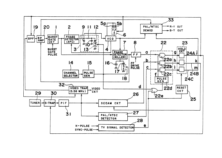
Referring to Fig. 2, a tuner 29 for receiving
television signals and producing a tuned television signal
is connected to a sound-trap 30 and then to a picture
intermediate frequency (PIF) 31. The output o~ the PIF
31 is connected to each of a SECAM circuit 26, a PAL/NTSC
detector 27 and a video trap 32. The video trap 32, which
is also coupled to a video circuit (not shown), is
connected to a band pass filter (BPF) 19 and hence to a
band pass amplifier 20. The band pass amplifier 20
produces a chrominance signal that is applied to a burst
gate circuit 1. The burst gate circuit 1 operates in
response to a bur~t gate pulse. The output of burst
gate circuit 1 is connected to a phase detector 2 for use
in an automatic phase controller (APC). A low pass filter
3 is connected to the phase detector 2 and to a voltage
controlled oscillator 4 which is coupled via a switching
circuit 6 to crystal vibrators 5a and Sb for
( oscillation at di~ferent frequencies, i.e. 3.58 MHz and 4.43
MHz, respectively. An automatic phase controller (APC) is
defined by a feed back loop containing the phase detector 2,
the low pass filter 3 and the VC0 4. Accordingly, the VC0 4
produces a subcarrier signal at a frequency of 3.58 MHz or
4043 MHz depending on the frequency of the burst signal, in a
manner that will be described in detail later.
According to the preferred embodiment, the low pass
filter 3 comprises a capacitor 9 connected between a hot
line, through which the signal transmits, and ground. Also,
a series connection of a resistor 11 and a capacitor 10 is
conneeted parallel to the capacitor 9. Furthermore, a series
connection of a capacitor 12 and a normally-closed switch 13
is connected parallel to the capacitor 10. Normally-closed
switch 13 is controlled by a pulse from a pulse generator 15
in a manner that will be described later.
The output of the VC0 4 is applied to a PAL/NTSC
demodulator 33 which produees an R-Y signal or a B-Y signal.
The output of the VC0 4 is also applied to a phase detector 7
whieh also reeeives the output signal from the burst gate
circuit 1.
According to a preferred embodiment, the phase
detector 7 is eonnected with ~ capacitor 16 which is grounded.
Also, a series connection of a capacitor 17 and a normally-
closed switch 18 is connected parallel to the capacitor 16.Normally-closed switch 18 is also controlled by a pulse from
the pulse generator 15 in a manner described below.
A channel seleetor 14 is eoupled to the puls~
generator 15. Whenever the broadcasting channel is changed
by the channel selector 14, the pulse generator 15 generates
a short pulse, such as shown by waveform d in Fig. 3. This
short pulse is applied to each of the normally-closed
switches 13 and 18 to open them temporarily during the
duration of the pulse. When the switch 13 opens, the
capacitor 12 is disconnected from the capacitor 10, thereby
making tile time constant of the low pass filter 3 short.
Similarly, when the switch 18 opens the time constant of
~z~
-- 8
( the phase detector 7 is shortened. When the time constant is
( shortened, the retraction operation of the APC loop occurs
faster, whereby the subcarrier wave for the newly selected
channel can be produced very fast from the VCO. This quick
response can be accomplished even when the channel change is
effected between two different broadcasting systems having
different subcarrier wave frequencies. Accordingly, a stable
subcarrier ~ave can be obtained immediately after the change
lQ of the channel.
The phase detector 7 is provided to produce a color
killer output which is applied to both a band pass amplifier
20 and the flip-flop circuit 8. When th~ VCO 4 is producing
a subcarrier signal having a frequency of 3.5~ ~z, the flip-
flop 8 generates HIG~ in response to the signal obtained fromthe phase detector 7. Similarly, when the VCO 4 is producing
a subcarrier signal having a frequency of 4.43 MHzl the flip-
flop 8 generates LOW. The output of the flip-flop 8, such as
shown in Fig. 3 at waveform a, is appli~d to an AND gate 22a
provided in a detection control circuit 22.
The detection control circuit 22 further includes
AND gates 22b and 22c and a pulse generator 22d. One input of
the AND gate 22b is connected to a SECAM circuit 26 which
produces HIGH when the received television signal is in the
SECAM system~ and LOW when it is not, such as indicated in
Fig. 3, waveform b. One input of the AND gate 22c is
connected to a PAL/NTSC detector 27 which produces HIGH when
the received television signal is in the NTSC system and LOW
when it is in either the PAL system or the SECAM system, such
as indicated in Fig. 3, waveform c. The other inputs of AND
gates 22a, 22b and 22c are connected to the pulse generator
22d. The pulse generator 22d has its input connected to an
OR gate 22e having two inputs. One input of the OR gate 22e
- is connected to the pulse generator 15 and the other input
thereof is connected to a television signal detector 28.
Details of the pulse generator 22d will be described later.
The television signal detector 28 has two inputs:
one for receiving the horizontal pulse; and the other for
receiving the sync-pulse. Accordingly, ~henever a television
signal, which may be obtained through an antenna (not shown),
cable (not shown), or from a video tape, is being received,
the television signal detector 28 generates a HIGH output,
such as shown in Fig. 3 at waveform e. The television signal
detector 28 produces LOW while the channel is being changed.
From this viewpoint, the signal produced from the television
signal detector 28 is similar to the signal produced from the
pulse generator 15, except that these two signals are in
opposite phase~ Furthermore, the signal from the television
signal detector 28 has the feature that, when a video tape is
being reproduced, the channel change recorded in the tape can
also be detected. Therefore, whenever there is a channel
change in the reproduced video tape, no pulse will be produced
from the pulse generator 15, but a pulse will be produced from
the television signal detector 28.
Accordingly, the OR gate 22e produces a signal not
only when the channel is actually changed, but also when a
channel change recorded in a video tape is detected.
As indicated in Fig. 3, waveform f, the pulse
generator 22d detects a step up of the waveform d or a step
up of the waveform e, and produces a one-shot pulse having a
pulse duration of t or t'. The AND gates 22a, 22b and 22c
are enabled only when a one-shot pulse is present, that is a
short period of time immediately after the channel change is
effected, which may be an actual channel change or a channel
change recorded in a video tape.
The AND gates 22a, 22b and 22c are connected to a
hold circuit 23 which is coupled to a reset circuit 25. The
reset circuit Z5 receives the signal from the television
signal detector 28 and produces a reset signal when the
channel is changed. Accordingly, when a new channel is
selected, the output signal from the AND gate 22a is h~ld in
the hold circuit 23, and is produced from the output terminal
24A of the hold circuit 23. Similarly, the output signal ~rom
the AND gate 2Zb is held and produced from the output terminal
24B, and the output signal from the AND gate 22c is held and
~a62æ3~:~
-- 10 --
produced from the output terminal 24C. Once the hold circuit
holds various data from the AND gates 22a, 22b and 22c
( immediately after the channel selection, this data is main-
tained as long as the selected channel is on.
Output terminal 24A, carrying data of the subcarrier
frequency, is connected to the switching circuit 6 for
selecting either one of the crystal vibrators 5a and 5b, and
also to the band pass filter 19, video trap 32 and sound trap
30.
Output terminal 24B, carrying data representing the
SECAM system, is connected to the SECAM circuit 26 for rlain-
taining the SECA~1 circuit operative while the received tele-
vision signal is in the SECAM system.
Output terminal 24C, carrying data representing the
PAL system or the NTSC system, is connected to the PAL/NTSC
demodulator 33 for actuating the demodulator 33. When the
received television signal is in the PAL system, the output
terminal 24C will produce LOW, thereby setting the demodulator
33 as a PAL demodulator. On the other hand, when the received
television signal is in the NTSC system, the output terminal
24C will produce HIGH, thereby setting the demodulator 33 as an
NTSC demodulator.
The operation of the circuit of Fig. 2 will now be
described. This circuit is operable with five different
broadcasking systems, namely: the PAL system with a 3.58 M~Iz
subcarrier wave; the PAL system with a 4.43 MHz subcarrier
wave; the NTSC syste~ with a 3.58 MHz subcarrier wave; the
NTSC system with a 4.43 MHz subcarrier wave; and the SECAM
system with 4.43 MHz.
It is assumed that the channel selector 14 is
actuated to select a television signal of the NTSC system with
the 3.58 ~z subcarrier wave. When the channel selector 14
is actuated, the pulse generator 15 produces a pulse (first
pulse in waveform d) which affects the pulse generator 22d to
produce a one-shot pulse tfirSt pulse in waveform f). While
the one-shot pulse is pxesent, the flip-flop 8 produces HIGH
indicating that the subcarrier wave has a frequency of 3.58MHz.
Also, the SECAM circuit 26 produces LOW indicating that the
received television signal is not in the SECA~I system, and the
PAL/NTSC detector 27 produces HIGH indicating that the
( received television signal is in the NTSC system.
Accordingly, when the one-shot pulse (first pulse
in waveform f) is produced from the pulse generator 22d, each
of the AND gates 22a and 22c produces HIGH (waveforms g and i),
and the AND gate 22b produces no pulse (waveform h). The
signals from AND gates 22a, 22b and 22c are produced in response
to the one-shot pulse, and are held in the holding circuit 23
which accordingly produces HIGH, LOW and HIGH, respectively,
from its output terminals 24A, 24B and 24C. These signals from
output terminals 24A, 24B, and 24C are maintained until the
reset circuit produces a reset signal, that is until the next
channel change.
The HIGH from output terminal 24A is applied to the
switching circuit 6 for selecting the crystal vibrator 5a for
oscillation at the frequency of 3.58 MXz. The HIG~ from output
terminal 24A is also applied to the band pass filter 19 for
selecting a band appropriate for the 3.58 MHz subcarrier wave,
and further to the video trap 32 and to the sound trap 30.
The LOW from output terminal 24B is applied to the
SEC~M circuit 26 to disable it.
The HIGH from output terminal 24C is applied to the
PAL/NTSC demodulator 33 to set it as a NTSC demodulator.
Since the data representing the system of the tele-
vision signal and the data representing the frequency o~ the
subcarrier wave are applied to the hold circuit 23 only when
the AND gates 22a, 22b and 22c are enabled, that is a short
period of time iINmediately after the change of channel, any
undesirable change or fluctuation in these data will not be
transmitted to the hold circuit 23 and to various other circuits,
such as the switching circuit 6. Accordingly, once the hold
circuit 23 holds the data of the received television signal
at the beginning of the channel selection, such data will not
be changed, even if the television signal fluctuates or noise
appears in the signal. Accordingly, the television receiver
not only automatically sets the circuit in a condition suitable
for the system of the received signal, but also maintains this
~2~æ~
- 12 -
set condition as long as the channel is maintained the same.
When a channel change is effected by the channel selector 14,
( or when a ch ~ el change signal recorded in a video tape is
reproduced, new data will be set and held in the hold circuit
S 23.
Signals produced from the output terminals 24A, 24B
and 24C for television signals received in different systems
are shown in the Table below.
Received Television Signal 24A 24B 24C
10 PAL 3.58 MHz subcarrier LOW LOW LOW
PAL 4.43 MHz subcarrier HIGH LOW LOW
NTSC 3.58 MHz subcarrier LOW LOW HIGH
NTSC 4.43 MHz subcarrier HIGH LOW HIGH
SECAM 4.43 MHz subcarrier LOW HI~H LOW
According to the embodiment shown in Fig. 2, the
detection control circuit 22 employs A~D gates 22a, 22b and
22c, but these AND gates can be replaced by other logic gates,
such as NOR gates, when the pulses applied to the gates are in
negative form.
Referring to Fig. 4, a modification of a subcarrier
generation circuit according to the present invention is shown.
The output of the flip-flop 8 is connected to an OR gate 34
which also receives a signal from a SECAM killer 35 in a
SECAM circuit. The output of the OR gate 34 is connected to
the switching circuit 6. Operation of this circuit is as
~ollows.
When a television signal of the NTSC system is
received, the flip-Xlop 8 produces HIGH in the manner described
above. This HIGH is applied through the OR gate 34 to the
switching circuit 6 to cause oscillation at 3.58 MHz by the
crystal vibrator 5a. Accordingly, the APC loop synchronizes
at the frequency of 3.58 MHz and the VCO therefore generates
a suhcarrier wave at 3.58 MHz.
When a television signal of the PAL system is
received, the flip-flop 8 produces LOW in the manner described
above. This LOW is applied through the OR gate 34 to the
switching circuit 6 to cause oscillation at 4.43 MHz by the
crystal vibrator Sb. ~ccordingly, the APC loop synchronizes
- 13 -
at the frequency 4.43 ~ and the VCO therefore generates a
subcarrier wave at 4.43 MHz.
( When a television signal of the SECAM system is
received, the SECAM KILLER 35 for the SECAM color killer
produces HIGH. Therefore, regardless of the signal from the
flip-flop 8, the OR gate 34 produces HIGH. Accordingly, the
switching circuit 6 is so turned as to oscill~ate at 3.58 MHz.
In this case, a subcarrier wave component at the frequency of
4.25 MHz or 4.406 MHz contained in the chrominance signal can
be applied to the phase detector 2. Since such frequencies
are much different from 3.58 MHz, the VCO 4 generates the sub-
carrier wave at 3.58 MHz without making any retraction operation
by the APC lo~p.
In this case, the color killer output produced from
the phase detector 7 can beused for disabling a color
processing circuit for the NTSC/PAL system and for enabling a
color processing circuit for the SECAM system.
Referring to Fig. 5, a circuit diagram of a low pass
filter is shown. According to the low pass filtar 3 shown in
Fig. 2, a series connection of capacitor 12 and normally-
close switch 13 is connected in parallel with the capacitor 10
to shorten the time constant when the switch 13 opens.
According to the modification shown in Fig. 5, a series connection
of a resistor 36 and a normally-open switch 13' is connected
parallel to the capacitor 10. Accordinyly, when a channel
change i5 effected, the switch 13' closes to shorten the time
constant. Accordingly, the low pass filter 3 shown in Fig. 2
can be replaced by the low pass filter 3 shown in Fig. 5.
Although the present invention has been fully
described with reference to a preferred embodiment, many
modifications and variations thereof will now be apparent to
those skilled in the art, and the scope of the present
invention is therefore to be limited not by the details of the
preferred embodiment described above, but only by the terms
of the appended claims.