Note: Descriptions are shown in the official language in which they were submitted.
~6~ 8B
-- 1 --
CRYOGENIC PACKAGING SCHEME
Background of the Invention
This invention relates generally to zero
force connectors for removably mounting large
integrated circuit~ such a~ Pin Grid Arrays (PGA)
whlch may have upwards of 200 pins and which are
immersed in liquid gases such as Nitrogen or Helium
for cooling and/or performance enhancement.
More specifically, this invention provides a
means and a method of packaging an electrical network
within a cryogenic vessel filled with a liquified gas
for cooling purposes. It also provides a means and a
method fox plugging and unplugging the electrical
device with ease at room temperatures, yet provides
for a sound, reliable electrical and mechanical
connection at cryogenic temperatures. A means is
provided to thermally isolate the immersed circuit
from the outside temperature by using a vacuum
insulation ves~el with carbon leads that thermally
isolate the interconnections.
A number of prior art patent~ deal with the
problem of cooling semiconductvr and with the problem
of making electrical connection~ to integrated circuit
package~ which packages are cooled either by imm~r~ion
into th~ cooling liquid or by heat sink~ which are in
contact with the cooling fluid. The following is a
representative listing of such prior art patents:
U.S. Patent No. 3,356,86~, entitled "ELECTRON
TUNNEL EMISSION DEVICE5 SYSTEMS" by I. Giaever;
U.S. Patent No. 3,365,620, entitled "CIRCUIT
PACKAGE WITH IMPROVED MODULAR ASSEM~LY AND COOLING
APPARATUS" by J. H. Butler et al.;
U.S. Patent No. 3,417,575, entitled "METHO~
OF AND MEANS FOR C~OLING SEMICONDUCTOR DEVICES" by
E.H. Stark;
~Z6..',~
U.S. Patent No~ 4,166,665, entitled "LIQUID
COOLED CONNECTOR FOR L~RGE SCALE INTEGRATED CIRCUIT
PACKAGES" by J. M. Cutchaw and
U.g. Patent No. ~,341,~32, entitled "LIQUID
C~OLED CONNECTION FOR INTEGRATED CIRCUIT PACKAGES" by
J. M. Cutchaw.
Summary of the Inventio_
The unique features of the present invention
are that it (1) provides for a method of
interconnecting an electrical network, or integrated
circuit which is immersed in a liquid, to a printed
cirruit board as~embly that is not immersed, (2)
provide~ for a means of plugging-in and unplugging a
many pin, "Pin Grid Array IPGA) Package" into a novel
socket with zero force (at room temperature) that will
provide solid reliable electrical and mechanical
interconnection at cryogenic temperatures below minus
38~8C using Mercury tHg) as a solder material, (3)
provides for a means of interconnection from a network
located in a cold cryogenic temperature to a room
temperature printed circuit board assembly using a
high electrical conductivity yet low thermal
conductivity media ~such as carbon) a~ a buffer media
to minimize thermal conduction out of the cryogenic
chamber through the electr.ical interconnection, and
(4) provides for a protective enclosure for the
cryogenic package to meet safety requirements.
In one preferred embodiment of the invention,
there is provided an integrated circuit package having
a plurality of electrical connecting pins and a vessel
for holding a low temperature liquified gas. The
vesæel is provided with a plurality of openings
th~rethrough corre~ponding to the plurality of
electrical pins of the integrated circuit package. A
plurality of pins having a cup end containing mercury
are mounted, one each, in the plurality of electrical
~ ~ ~ 2,~
pins of the integrated circuit package prior to the
addition of the low temperature liquified gas. The
plurality of electrical pins are securely connected to
the plurality of pins having a cup end by adding a low
temperature liquified gas to the vessel to solidify
the mercury in each of the cup ends of the plurality
of pin~. ~n electrically conductive and thermally
insulating material is used to connect the plurality
of cup Pnd pins to circuitary external of the vessel.
Accordingly, it is a primary object of the
prPsent invention to provide an improved cryogenic
packaging assembly.
It is another object of the present invention
to provide an integrated circuit package mounting
which permits easy insertion and removal to and from a
circuit board.
Still another object of the present invention
is to provide interconnections between an electrical
circuit located in a low temperature environment and
electrical circuits located in a higher temperature
emvironment.
The~e and other objects of the present
invention will become more apparent when talcen in
conjunction with the following description and
drawing~ wherein like characters indicate like parts
and which drawings from a part of the ~resent
disclo~ure.
Brief Description of the Drawings
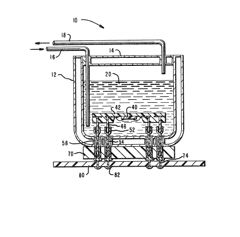
Fig. 1 is a full sectioned view of the
preferred embodiment of the invention.
Fig. 2 is an enlarged view of a portion of
the preferred embodiment of Fig. 1.
- 4
Detailed Descri lon of the Pre red Embodiment of
the Invention
Referring to Figs. 1 and 2, the cryogenic
packaging for an IC chip is shown generally as item
10. Th~ cryogenic packaging 10 is comprised of a
vessel 12 which may be a Dewar vessel having a closed
but removable top 14 into which vessel is placed a low
temperature liquified gas 20 such as Nitrog~n, Freon,
Argon and Helium. Within the vessel 12 is positioned
an IC chip 40 mounted in a package 42 having
electrical conductors 44 and which package has a
plurality of electrical connecting pins 46 extending
therefrom. A corresponding plurality of openings 58
are formed through the wall of the vessel 12. A
corresponding number of pins 50 having an open
receiver portion 52 shaped as a cup are embedded in an
electrically conductive and thermally insulated
material 54 which fills the openings 58. The open
receiver 52 i5 partially filled with Mercury 60~ The
material 54 may be carbon which functions as a buffer
media to minimize thermal conduction out of the
cryogenic chamber through the electrical
interconnections. A corresponding plurality of
electrical pins 56 are inserted into the carbon
material and extend outwards from the vessel 12.
These electrical pins are configured and positioned so
as to mate with connector pins 72 mounted in a
receiving socket 70. Each of the pins 72 has a
projecting segment 74 designed to mate with conductors
on a PC board ~0 and ~o be soldered to a conductor at
82.
To insert the IC chip 40 through its mount 42
carried connecting pins 45 into the open receivers 52
with a zero force, the temperature of the Mercury 60
is raised so that it is more positive than minus
38.8C ~ince the Mercury in the connector pins is in a
liquid state at these temperatures. The IC chip 40
~L2~
-- 5 --
can then either be inserted and/or removed and a new
IC chip inserted without the necessity of unsoldering
all of the connectors. Once the IC chip is in place,
the temperature is lowered causing the mercury to
solidify, thus forming an electrical and mechanical
connection similar to that of tin/lead eute~tic
solder. Th tub 18 extending through the top 14 of
the vessel 1~ is used to take off the liquified gas
commonly called the boil-off so that the gas can be
repro~essed to form it back into a liquid and to
reinject it, via the tube 16, back into the vessel 12.
~ hile there has been shown what is considerPd
to be the preferred embodiment of the invention, it
will be manifest that many changes and modifications
may be made therein without departing from the
essential spirit of the invention. It is intended,
therefore, in the annexed claims, to cover all such
changes and modifications that may fall within the
true scope of the invention.