Note: Descriptions are shown in the official language in which they were submitted.
1490.2 ~ 'd.~3~
--1 --
FIELD OF THE_INVENTION
This invention relates to solid-state
overvoltage protection devices, and in particular to
thin film semiconductor devices and structures
utilizing substantially amorphous threshold switching
material for suppression of high speed transients.
BACKGROUND OF THE INVENTION
The need to protect electronic circuitry from
overvoltages, especially ~ransient overvoltage
conditions, is well known. Most electronic components
are only built to withstand the application of cer~ain
limited voltages across them, and will be damaged or
seriously malfunction if higher voltages are applied.
There are many sources of ~ransient
overvoltages, such as lightning, electrostatic
discharge (ESD), electromagnetic induction (EMI).
Failure of circuit components may also allow excess
voltages to be applied across other circuit
components. Inductive surges are yet another source
of overvoltage transients.
Lightning, ESD and inductive surges are all
capable of producing very rapid high voltage
transients. An inductive surge produced by
interrupting a running 115 volt motor can be as high
as 1,000 volts or more, for example. Electrostatic
discharges, such as those produced by a person walking
~0 on a wool rug on a dry winter day, can easily result
in a charge of tens oF ~housands of volts. Although
such electrostatic discharges usually involve a
relatively minor flow of current, ~hey, like inductive
surges, are sufficient to destroy many types of
microelectronic circuits. ~vervoltage transients
caused by lightning can deliver by direct strikes
large amounts of currents at tens of thousands to
hundreds of thousands of volts. By E~I, lightning can
1490.2
generate high voltage transients in the megahertz
frequency and higher ranges.
Conventional means for dealing with
relatively small overvoltages include shunting
capacitors, breakdown diodes, varistors and inductive
coils. Breakdown diodes such as zener diodes when
reverse biased beyond a certain threshold voltage
conduct large currents. Like virtually all
overvoltage protection devices, such a diode is placed
ahead or "upstream" of or in parallel with a circuit
element to be protected, and shun~s excess voltage
applied thereacross to a discharge path such as a
neutral line, D.C. common line, chassis or ground.
However, such diodes are capable of only handling
limited overvoltages without becoming permanently
damaged themselves.
Varistors, which are typically made of
pressed powders, ac~ somewhat like zener diodes, in
that they offer a high impedance at low voltages and a
2U relatively low impedance at high voltages. However9
they are distinguished from zener diodes in that their
current characterlstics are symmetrical rather than
asymmetrical, and thus can offer protection against
overvoltage in both directions.
Inductive coils or chokes, while unable to
protect circuitry from low frequency or sta~ic
overvoltages, do tend to filter out rapid voltage
transien~s by presenting a large impedance. Since
they also present high impedance to high frequency
signals, they are inappropriate for protecting high
frequency circuitry from high frequency overvoltages.
Such chokes are also normally relatively bulky and
expensive.
Spark gaps are another form of overvoltage
protection associated with higher power devices, and
recently miniaturized forms of them have been
1490.2 ~2~
-3-
developed for use on P.C. boards and the like. Spark
gaps contain two opposing electrodes separated by a
nonconductive gas, such as air, which has a desired
breakdown, or sparking vol~age. When an overvoltage
is applied across the spark gap, the nonconductive gas
becomes ioni~ed, forming a relatively low resistance
path between its electrodes. Although spark gaps have
beneficial uses, ~hey usually are not very appropriate
for use in solid-state circuitry because they are not
solid-state devices and because they are usually
fairly large, even in miniaturized form. Also the
time required for the opera~ion of spark gaps is
usually too slow to provide full protection from
extremely rapid transients.
Varistors, inductive coils and spark gaps all
share the same shortcoming--they cannot be readily
incorporated into microelectronic devices due to the
required way in which they must be made.
Several types of integrated circuits, CMOS
for example, are notoriously sensitive to static
electricity, particularly before being inserted into a
larger circuit on a P.C. board. Furthermore, the CMOS
circuits themselves are typically unable to handle any
significant power, so that it is difficult and
expensive to arrange on-chip protection by exclusively
dedicating certain portions of the chip to such a
protection function. Thus, there is a definite need
for extremely high speed and/or high power protection
that can be readily incorporated direc~ly into all
3U types of microelectronic circuitry, as an integral
part thereof, to protect such circuitry at all timesO
As a result of the nuclear age a new and very
threatening source of overvoltage transients is made
possible by the phenomenon known as the nuclear
electromagnetic pulse or "EMP". EMP will be produced
by the Compton electrons scattered by gamma rays from
14gO 2 ~ 3
--4--
a nuclear explosion colliding with air molecules of
the upper atmosphere. Theoretical studies have
indicated that if a nuclear device were exploded at a
high altitude above most of the earth's atmosphere a
large EMP generated therefrom would have sufficient
intensity to induce a large current in conductors
hundreds or thousands of miles away to destroy
electronic e.quipment connected to or containg such
conductors.
EMP jc particularly difficult to protect
against for three reasons~ the extremely rapid
rise time; (23 the expected intensity, and (3) the
ubiquitious presence, î.e., all conductors of any
appreciable length n~t enclosed with a sui~able
Faraday shield will act as an antenna, and thus be
subject to severe electrical transients due to the
EMPi It has been estimated that EMP will produce an
extremely high overvoltage within approximately one
nanosecond or less and reach a peak field in only
about 10 nanoseconds, before trailing off in about one
microsecond. The peak field produced by a one-megaton
warhead exploding in the upper atmosphere may be as
high as 50,000 volts/meter. Further de~ails about the
nature of EMP and the Inadequacies of conventional
overvoltage protectlon devices to protect a~ainst them
is found in "Electromagnetic pulses: potential
crippler," IEEE Spectrum, May, 1981, pp. 41-46.
Most conventional solid-state overYoltage
protection devices are too slow or limited in their
3U power handling capabilities to provide full protection
against the effects of very close lightning strikes or
EMP. This is because such lightning strikes and EMP
can produce overvoltages two or three orders of
magnitude or more above the normal operating voltages
of the integrated circuits subjected to such
transients, thus leading to enormous current surges
1 490. 2 :~,2~
--S--
capable of destroying virtually almost all types of
solid-state semiconductor protection devices. As the
energy content of such pulses is increased, the
problem becomes more severe, and requires extremely
rugged, high ampacity overvoltage protection devices,
preferably incorporated at the integrated c~rcuit
level 9 to handle any ~ransients which reach such
microelectronic circuits. As the size of
microelectronic circuit elements is reduced, the
problem also becomes more severe since less energy is
required to damage smaller devices. To avoid creating
problemsg overvoltage protection devices, when
inserted into or included as part of the electronic
circuit to be protected, must not impose undue
insertion losses in the c~rcuit3 or decrease switching
speeds or band width by adding s~ynificant amounts of
capaci~ance.
One class of overvoltage protection devices
which has long held great potential for very high
speed transient suppression applications are Ovonic
threshold switching devices of the type first invented
and announced by S.R. Ovshinsky in the 1960's. U.S.
Patents Nos. 3,171,591 (1966) and 3,343,034 to S.R.
Ovshinsky (1967) specifically teach that this type of
khreshold switching device ~s suitable for use as
surge suppressors, such as for transient inductive
pulses and the like. Such switches have been known
since at least 1968 to have a switching speed of less
than 150 picoseconds, see, e.g., S.R. Ovshinsky,
"Reversible Electrical Switching Phenomena ln
Disordered Structures", Physical Review Letters, Vol.
21 3 No. 20, Nov. 11, 1968, p. 1450(c).
R. Callarotti, et al.g "Transmission Line
Protection With Thin Film Chalcogenide Glass Devices,"
Thin Solid Films, Vol. 90, pp. 379-384 tl982), suggest
that an Ovonic threshold switch of a thin film of
~2~;2.f .. ~
chalcogenide ylass is well suited Eor protecting a
transmission line from EMP. A detailed mathematical analysis
is presented therein in support of this view.
A number of overvoltage protection devices using
Ovonic threshold switching materials have been proposed.
These devices include various electrical connectors with
Ovonic threshold switches providing a path for shunting
transients to the connector casings, and integrated circuits
and printed circuit boards having a thin film of Ovonic
threshold material overlying the top wiring layer for
providing protection for all conductors forming part of the
top wiring layer. These devices are intended for use in
protecting against EMP, ESD and other high voltage
transients.
Ovonic threshold switching devices may be generally
described for the purposes used herein as a switching device
which has a bistable characteristic, including a threshold
voltage and a minimum holding current. Specifically, the
device includes a semiconductor material and at least a pair
of electrodes in contact therewith, wherein the semiconductor
material has a threshold voltage value and a high electrical
resistance to provide a blocking condition ~or substantially
blocking current therethrough, and wherein the high
electrical resistance in response to a voltage above the
threshold voltage value very rapidly decreases in at least
one path between the electrodes to a low electrical
resistance which is orders of magnitude lower than the high
electrical resistance, which provides a conducting condition
or path for conducting current through the semiconductor
material. The conducting condition or path is maintained in
the
rn/jj
, 1490-2 ~6~
--7--
device so long as at least a minimum holding current
cQntinues to pass through the conducting path within
the device. When the current falls below this m~nimum
current value, the device rapid1y reverts to its high
resistance blocking condi~ion. The voltage drop
across the sem;conductor material in a threshold
switch when in its conducting condition is a fraction
of the voltage drop across the material when in its
high electrical resistance blocking condition, as
measured near the threshold voltage value of the
switch.
Many different combinations of chemical
elements when combined ln the proper proportions and
manner have been shown to produce a semiconductor
material having the aforementioned threshold switching
action. Most commonly, chalcogenide glasses, such as
Te39A536Si 1 7Ge7Pl 9 are used. Examples of
such materials and threshold switching devices made
therewith are found ln the follow~ng list of U.S.
~0 patents, all of which are assigned to the assignee of
! the present inventlon: ~ ~
3,271,~91 3,571,~71
3,343,034 39571,672
3,571,669 3,58~ 3 638
3,571,670 3,611,063
Threshold switches are generally arranged as
two terminal devices, and have been shown in a number
of configurations, including one having a pair of
electrodes arranged in the form of interleaving
metallic fingers or combs (see Figure 7 of U.S. Patent
No. 3,271,591 to S.R. Ovshinsky). Since they exhibit
symmetr;cal current-voltage (I-V) characteristics,
have been applied typically in alternating cllrrent
l490.2
--8--
applications. They are ambipolar dev;ces, that ;s the
current in the conduction path consists of both holes
and electrons. They can have extremely high current
densities. If driven properly, threshold switches can
have extremely fast sw~tching speeds, such as into the
nanosecond region and below, and make excellent surge
suppression devices. Typically, a threshold switch is
constructed of a thin film of preferably amorphous
semiconductor material, and may be described as a
semiconduc~ing glass3 although there are a number of
other forms of threshold switches such as those
described in U~S. Patent No. 3,715,634 to S.R.
Ovshinsky. Two termlnal threshold devices, once
turned on, cannot be turned off, except by reducing
the current through the device` below its minimum
holding current for the requisite period of time,
which is typically well under one microsecond.
The aforementioned patents and patent
application, while disclosing a number of useful
structures and configurations for Ovonic threshold
switching devices in a variety of applications, do not
disclose how to optimize the design of swch devices
for high power, extremely high speed applications. In
particular, the foregoing references do not
spec~fically teach any method for avoiding localized
concen~rations of currents in the threshold switching
material which have been known to be of such intensity
as to ablate the material or electrodes in contact
therewith. The paten~s also do no~ teach how to scale
up the size of integrated threshold switching devices
so that the devices may reliably be used to handle
transient currents in excess of several hundred
milliamps, such as 5 amps, lO amps or above,
1490.2
SUMMARY OF THE INVENTION
The objects of the present invention are to
prov;de an overvoltage protection device or apparatus
which has at least several of the following
attributes: (1) capable of being scaled up to handle
relatively large currents; (2) highly efficient
thermal design to allow for dissipation of heat due to
the shunting of current produced by extremely large
overvoltages; ~3) produces minimum insertion losses
when in use, and has minimal capacitance, (4) has
multiple current paths for shunting current through a
threshold switching material, including redundant
interconnections to such current paths for increased
reliability; (~) capable of extremely high speed
operation; and (6) presents minimum inductance when in
use to facilitate such high speed operation.
Another important object o~ the present
invention is to provide and overvoltage device
~o structure which is capable of confining a filamen~ary
current into one or more selected elongated current
conduction channels, as a means of obtaining a
structure we11 suited for handling large transient
currents and dissipating any heat generated khereby.
In light of the foregoing objects, one aspect
of the present invention provides a solid-state
overvoltage protection apparatus of the type having a
plurality of spaced electrodes and a body of threshold
switching material disposed ~herebetween, said body
having (1) a high electrical resistance to provide a
blocking condition for substantially blocking current
kherethrough at operating voltages below a first
nominal level, and (2) a lower electrical resistance
at overvoltages above the first nominal voltage level
to provide a conducting condition for conducting
current there~hrough. The improvement çomprises in
~2~
1490.2
-1 0-
combination: means for providing an elongated current
conduction path of substantially uniform distance
between ~he electrodes through the body where the
current conducting path is confined to an elongated
cross-sectional area of the body transverse to the
direction of current flow. The cross-sectional area
has an effective length along the major dimension of
the body which is at least about ten times greater
than ~he maximum effected width of the body. In this
way the relatively large currents associated with
overvoltages are distributed over said elongated area.
The elec~rodes in the apparatus may each have
an elongated surface portion adjacent to and in
intimate electrical contact with the body of threshold
switching material. The elongated surface portions of
two facing electrodes (separated by the threshold
switching material) are equidistantly spaced from each
other thereby providing the elongated current
conduction path of substantially uniform distance
~o therebetween.
The apparatus may also include a highly
thermally conductive substrate disposed below said
threshold switching material. The substrate may be
formed from an electrically conductive metalcovered
with an insulating layer, or may be formed from an
insulating material.
The overvoltage protection devices of the
present invention may have vertical, horizontal or
diagonal current conduction paths through the body of
3~ threshold switching material. At least one of the
electrodes and the threshold switching material may be
patterned to form a mesa structure. Alternatively the
overvoltage protection devices or apparatus of the
present invention may include a layer of insulating
material having an elongated opening therein in which
at least a portion of said`threshold switching
1490. 2 12~a?,~
material extends, and wherein one of said electrodes
is disposed substantially in said opening, and another
of said electrodes is disposed above said portion of
said threshold switching material in said opening,
such that when the current conduction path is formed
in the apparatus it extends vertically between the
electrode portion through said portion of threshold
swi~ching material disposed in said opening.
The apparatus of the present invention may
also have at least one of the electrodes formed from a
thin film layer of conductive material patterned to
have a plurality of electrically interconnected
sections spaced apart from one another at
predetermined angles. For example, such patterned
electrode-forming layers may include at least three
leg sections interconnected at a common central node
section which each extend outwardly therefrom in a
direction different from the other two leg sections.
The patkerned layer may further include a plurality of
common node sections interconnected by at least one of
sa1d leg sections.
In the various devices of the present
invention, at least a portion of said body of
threshold switching material preferably has the
property that it changes from a hiyh resistance state
to a low resistance state when the voltage applied
across it exceeds a given threshold voltage and
maintains that low resistance state as long as a
certain minimum maintanence voltage substantially less
3~ than the threshold voltage is maintained across it.
This characteristic of Ovonic threshold switching
material makes it ideally suited for handling high
power transients, since it minimizes the generation of
heat within an overvoltage protection device, and also
acts to clamp the overvoltage to very low levels.
1490.2 ~ ?".
-12-
Other aspects, objects, features and
advantages of the present invention will become
apparent from the subsequen~ description and the
appended claims taken in conjunction with the
accompanying drawings.
BRIEF DESCRIPTION OF THE DRAWIN6S
Figure 1 is a partial side view in
lo cross-section of an electrical device of the present
inventionu
Figure 2 is a partial side view in
cross-sec~ion of two electrical devices of the present
inYention, each having a mesa structure disposed on a
common bottom electrode.
Figure 3 is a partial side view of two
al~ernative mesa structure devices of the present
invention which are electrically isolated from one
another.
Figures 4A, 4B and 4C are partial side views
of electrical devices of the present invention having
a vertical conduction path formed through an opening
in an insulating layer;
Figure 5A is a partial plan view of another
electrlc devlce of the present invention which has a
fully encapsulated active region, and Figure 5B is an
enlarged cross-sectional side view taken along line
SB-5B in Figure 5A.
Figure 6 is a side view in cross-section of a
3~ horizontally arranged electrical device of the present
invention~
Figure 7 is a side view of an electrical
device of the present invention having a diagonal
current conduction path.
Figures 8A and 8B are side views of the
Figure 6 device when partially constructed
1~90.2
~Z~f.~
-13-
illustrating its me~hod of cons~ruction.
Figure 9 is a partial s;de view of an
electrical device of the present invention having a
diagonal current conduction path.
Figures 10 and 11 are side views of the
Figure 9 device at different stages of partial
construction.
Figure 12 is a partial side view of an
electrical device of the present invention similar to
that of Figure 9, but with less capacitance.
Figure 13 is a partial plan view of an
elertrical device of the present invention having
interdigitated electrodes.
Figure 14 is a plan view in another
embodiment of the present invention illustrating
bifurcation of an expanding current filament.
Figure 15 is a plan ~iew of another
embodiment of the present invention having redundant
electrode interconnections.
Figure 16 is a plan view of an electrical
device of the present invention having a serpentine
current conduction channel.
DETAILED DESCRIPTION OF THE PREFERRED EMBODIMENTS
_
F~gures 1 through 12 are cross-sec~ional side
views of the several electrical devices of the present
invention all of which can be configured as
overvoltage protection devices to suppress high speed
transients. Most of these devices are particularly
well suited for forming high power overvoltage
protection devices due to their highly efficient
thermal design which makes it possible to control and
quickly dissipate any heat which may be developed from
handling high transient or even moderate continuous
overvol~ages. Figures 13 through 16 show various
1490.2
possible plan views of the electrical devices of the
present invention, virtually all of which provide for
efficient distribution of any heat generated in the
device to highly thermal conductive substrates and/or
electrodes where it can be harmlessly dissipated.
The preferred embodiments of the devices of
the present invention shown in Figures 1 through 12
are current-carry~ng solid-state semiconductor devices
having a plurality of metallic electrode layers, a
plurality oF thin film layers of carbon material
associated with the electrodes, and a body or layer of
semiconductor material in intimate electrical contact
with the thin films of carbon material. Each of the
electrodes are in intimate electrical contact with its
respective thin film of carbon material such that
current flows into one electrode through its layer of
carbon material tllrough the semiconductor material
into the second layer of carbon material and from
there into ~he second electrode. (Although not
~o preferred, the devices of the present invention may
also be constructed without the carbon films, provided
that the remaining electrode layer ~n contact with the
semiconductor layer is fully compatlble with the
semiconductor material.)
It is worth noting that AppLlc~nt's Canadian
l~pl:L~atlon Serial No. 546,589, filed September 10, 1987, `
and entitled "Thin Film Electrical Devices
With Amorphous Carbon Electrodes And Method Of Making
Same" discloses and hroadly claims various aspects of
the subject matter of Figures l through 8B presented
below.
` In the Figures, there are shown several
electrical devices of the present invention all of
which are current-carrying solid-state semiconductor
devices having a plurality of electrodes, a plurality
of thin films of carbon material associated with the
~.
1490.2
-15-
electrodes, and a body or layer of semiconductor
material in intimate electrical contact with the thin
films of carbon material. Each of the electrodes are
in intimate electrical contact with its respective
thin film of carbon material such that current flows
into one electrode through its layer of carbon
material through the semiconductor material into the
second layer of carbon material and from there into
the second electrode.
1~ Referring now to Figure 1, there is shown an
electrical device 30 of thP present invention which is
preferably a thres~old switching device, and which
utilizes a pair of conductive films of carbon material
as barrier layers disposed between a center layer of
semiconductor or active material and upper and lower
metallic electrodes. Each film of carbon material may
be considered as part of the electrode to which it is
adjacent. The device 30 is formed on a substrate 32
which may be conductive or insulating, as required for
the device application. Stainless steel, copper, and
aluminum are examples of suitable conductive
substra~es, while glass, crystal silicon and crystal
sapphire wafers are examples of insulating
substrates. Successively deposited above the
substrate 32 are a region or layer 34 of electrode
material, a film 36 of carbon material, a body or
layer 38 of semiconductor or active material, an upper
region or film 40 of carbon material, and a top me~al
electrode 42.
The electrodes 34 and 42 are preferably
formed of molybdenum, although they can be any other
suitable highly conductive material, preferably those
with high melting points and which are relatively
inert with respect to the semiconductor material of
layer 38, such as tantalum, niobium, tungsten9
molybdenum, and tantalum-tungsten alloy. The films 36
1490.2
l ~
and 40 are electrically conductive,
non-single-crystal, phase-stable, non-switching carbon
material. The thin film 36 is in intimate electrical
contact with the electrode 34 at interface 44 and with
the sem~conductor layer 38 at interface 46. The film
40 of carbon material is in intimate elec~rical
contact with the semiconductor layer 38 at interface
48 therebetween, and with upper electrode 42 at
interface 50 between film 40 and electrode 42.
The electrode layers 34 and 42 may be
deposited using any conventional or suitable technique
such as sputtering, evaporation, vapor deposition, or
the like. Preferably, the electrode layers are
deposited as amorphous films by maintaining the
tempera~ure of ~he surface upon which ~hey are being
deposited sufficiently cool, so that the atoms
condense into a generally disordered or amorphous
state upon contacting the deposition surface.
The films of carbon material 36 and 40 are
preferably deposi~ed using DC magnetron sputtering.
Typical process parame~ers are a substrate temperature
of about 100 degrees C, a pressure of 0.5 p~scal, a
deposition rate of 200-300 angstroms per minute, and a
distance of approximately 6 centimeters between source
and target. The resultant film of carbon material
hich results under these conditions is unlformly
amorphous (a-carbon). Preferably, a pure carbon
source is used so that the resultant film is
substantially pure carbon. As used herein, pure
carbon source means a source of material ~hat is at
least 99.9 percent carbon and preferably is 99.99
percent more pure carbon. When amorphous carbon is
sputtered under such conditions, it may have a
resistivity as low as about 0.25 ohm-centime~ers.
More detailed information abou~ the process
for sputtering such conductive thin films of
1~90.2
-17-
substantially amorphous carbon, and the electrical and
structural characteristics of such films is provided in
N. Savvides, "Four-fold to Three-fold Transitisn in
Diamond-Like Amorphous Carbon Fllms: A Study of
Optical and Electrical Properties", Juurnal of Applied
Physics, Yol. 58, No.l, ppO 518-521 (July, 1985)-
The threshold switching material or otheractive material of layer 38 may be deposited wsing any
suitable or conventional ~echnique well-known to those
in the art. The preferred threshold switching
materials used for layer 38 in the Figure 1 device
(and in the active layer of the devices shown in the
other Figures) are films of amorphous semiconductor
material which include one or more chalcogenide
elements, i.e., sulphur, selenium and tellurium.
(However, any type of semiconductor material which
exhibits suitable switching oehavior useful for
overvoltage protection, voltage clamping or other
~0 electronic applications may also be used in the
devices of the present invention.)
A preferred compos~tion for layers 34-42 of
device 30 when device 30 is used as a thin film
threshold switching device is disclosed in Table I
below. Table I llsts exemplary materials and
exemplary ranges of thicknesses for threshold
swltching dev~ces of Figure 1 and the other figures.
A typical thickness for sample devices constructed and
tested are also given. The thickness values are in
3U angstroms.
1490.2 ~2~
-18-
TABLE I
Reference Exemplary Range of Typical
Numeral- Material Thicknesses Thickness
42 molybdenum1,500 - 25,000 5,000
a-carbon100 - 2,000 1,000
38 Te3gAs36sil7Ge7pl
36 a-carbonlQ0 - 2,000 1,000
34 molybdenum1,500 - 25,000 5,000
In fabricaking device ~0, it is highly
preferred to deposit the layers 34 through 42 in
sequence while substrate 32 is continuously ma~n~ained
under a partial vacuum. This helps ensure that
extremely clean interfaces are formed between the
layers, and greatly reduces the chance for any
appreciable amount of contaminants such as alr, water
vapor, dust or the like to contaminate the
interfaces. Thls not only helps ensure fine physical
integrity of the interfaces 44-50, but also helps
ensure the formation of high quality electrical
interfaces between ~he layers. Such clean interfaces
are believed to help greatly reduce possible localized
heating effects and nucleation si~es for undesired
localized crystallization of the semiconductor
materials, which may well adversely affect the
electronic repeatability and long-term stability of
the device.
As indicated in Table I, the layers 34-42 and
device 30 are preferably thin film. As used herein,
the term "thin film" typically refers to a film having
a thickness of less than five microns. Those in the
1490.2
l g
art will apprecia~e, however, that for certain
applica~ions it is possible to scaleup the indicated
thicknesses of the embodiment of the present invention
so that at least some of the layers, such as the
semiconductor layer 38 or electrode layers 34 and 42,
may be thicker than five microns.
The thickness of the semiconductor film
(layer 38) is related to the specified threshold
voltage (VTH) which is desired, and may be adjusted
in a manner well understood in the art. On the
average, the threshold voltage of threshold-type
semiconductor ma~erials such as that listed in Table I
is approximately lS volts per micron of conduction
path length. Therefore, in order to ach~eve a
threshold voltage on the order of 8 to 9 volts in a
vertical threshold device of the type shown in Figure
1, for example, layer 38 is made approximately 5200
angstro~s to 6000 angstroms thick.
The thickness of the various thin films used
in the Figure 1 structure, as well as the other
structures of the present invention, may be readlly
controlled using any one of several techniques well
known in the art. Those in the art will readily
appreciate the threshold voltage of the device 30 may
be made much higher or much lower simply by increasing
or decreasing the thickness of the semiconductor layer
38.
In operation of the electrical device 30,
current from its first elec~rode passes thr~ugh at
3~ least one portion of the first carbon layer, through
at least a filamentary path or portion of ~he
semiconductor material and through the second carbon
film to the second electrode. Since current takes the
path of least resistance~ which should always be
through the shortest or more direct route through
material of uniform resistivity, the current
~iL2
o . 2
-20-
conduction path in the thin carbon films 36 and 40 and
the semiconductor layer 38 of Figure 1 should be
substantially vertical.
While the basic device structure shown in
Figure 1 clearly has utility for many applications, it
has been found desirable in certain applications to
pattern some or all of the layers in the multiple
layer structure shown in Figure 1 into mesa
structures, as is shown by way of example in Figures 2
and 3.
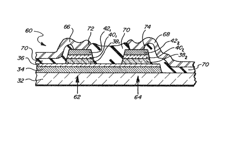
The Figure 2 shows a thin film structure 60
including tWQ mesa structures 62 and 64 arranged on a
common substrate 32. The mesa structures 62 and 64
have conductors 66 and 68 respect7vely connected to
their upper electrodes. The mesa structures 62 and 64
represent two distinct threshold switching devices
having a common electrode. The overall structure 60
may be constructed by suitably patterning a multilayer
structure 30 of Figure 1 using conven~ional or
suitable lithographic and etching techniques. The
structure 60 includes a common electrode 34 and a
common f~lm of carbon material 36. In particular, the
mesa structures 62 and 64 are ~ormed by patterning
layers 38, 40 and 42 into distinct sets of layers
381, 401, 421 and 382, 42~ 422, as shown
1n Figure 2. Once layers 38 through 42 have
patterned, an insulating layer 70 is deposited over
the entire structure. Layer 70 may be any suitable
deposited thin film insulating ma~erial such as
silicon oxide ~SixOy)~ silicon nitride (SiXNy)
or preferably siliconoxynitride (SiOXNy). Layer
70 may range in thickness from about 0.3 to 2.5
microns depending in part on the combined thickness of
layers 38-42, and is preferably about 0.6 micron thick
for the typical thicknesses of layers 38-42 shown in
Table 1. After layer 70 has been deposited
1490.2 ~ 2 ~
conventional photolithographic and etching techniques
are used to create openings or vias 72 and 74 therein
above mesa structures 62 and 64. Thereafter~ a top
metallization layer is deposited over the entire
structure 60 and may be patterned so as to provide
individual conductive lines 66 and 68 ~o mesa
structures 62 and 64, thereby allowin~ them to be
accessed as separate electrical devices. Layer 34, as
well as traces 66 and 68 may be connected to other
thin film devices connected on the same substrate or
to terminal pads (not shown~ to provide easy
connection to the threshold switching devices 62 and
64. The etching of the various thin film layers of
structure 60 may be accomplished using conventional or
suitable etchants, either wet or dry, known to those
in the art.
Figure 3 shows a thin film structure 80
containing two mesa structures 82 and 84 which include
more pa~terned layers than do the mesa strucl:ures of
Figure 2. Specifically, layer 34 is shown partially
etched away to form conduct~ve pads 341 and 342
for mesa structures 82 and 84 respectiv~ly. These
pads serve as the lower electrodes. Similarly, thin
film carbon layer 36 has been etched into portions
361 and 362 as shown. The remainder of the
processing steps may be carried on as previously
described with respect to Fi~ure 2 in order to create
distinct portions of layers 38, 40 and 42 . The 1 ower
electrode 341 of structure 82 i s shown extending to
3U the left so that contact may be made thereto at a
portion 86 thereof. The lower electrode portion 34
may be similarly extended in any direction, space
permittin3, to provide an electrical contact thereto.
Thus, in mesa structures 82 and 84 both electrode
layers, both carbDn f~lm layers and the semiconductor
layer have been patterned, so as to form a completely
1490.2
-22-
isolated threshold switching device. If desired the
top metallization layer, which is shown patterned into
traces 66 and 68, can be interconnected by a
connecting portion of 90 which can be patterned at the
same ti~e as conductor 66 and 68. In this manner,
devices 66 and 68 can be connected in parallel if
desired for increased current-carrying capability or
for any other circuitry purpose.
Thin film structure 100 of Figure 4A is
another vertical embodiment of the present invention.
In addition to the layers 34 through 42 pre~iously
mentioned, structure 100 features two additional
layers, namely an insulating layer 102 which has an
opening or pore 104 ~herein and an addit;onal, very
thin layer of carbon film 105 deposited on top of
insulating layer 102. The layers 102 and 106 are
sandwiched between the thin film carbon layer 36 and
semiconductor layer 38, as shown. The horizontal
length 108 of the opening 104 may be any desired size
~0 such as ten microns, five microns, or less. The
thickness of insulating layer 102 may range from 1,000
to 10,000 angstroms or more and preferably bet~een
2,400 to 6~000 angstroms. A highly conductive top
metallization layer 110, preferably made of aluminum
and on the order of 0.5 microns to about 2.0 microns
thick, and in intimate electrical contact with upper
electrode 42 may be provided if desired to increase
ampacity of electrode 42 and improve heat
dissipation. Like in the Figure 4B device, the
structure 100 of Figure 4A may be patterned into a
mesa structure if desired simply by etching ~hrough
the various layers a sh~rt distance (such as 2 to 10
microns) outside of the top lef~ edge 112 and top
right edge 114 of the opening 104.
The mesa structure 118 shown in Figure 4B is
formed using the same basic structure 100 shown in
l490.2 ~2~2,~
-23-
Figure 4A, except that layers 106, 33 and 40 may be
patterned as shown prior to the deposition of layer
42. When layer 42 is deposited, it overlies and
extends beyond the mesa structure formed by patterned
layers 106, 38 and 40, thus providing a cap or
passivation layer which acts to hermetically seal the
layers 106, 38 and 40 from possible exposure to
adverse environmental conditions. Thereafter, the top
metallization layer 110, which is preferably aluminum,
may be deposited, and if desired, patterned into a
suitable shape for a cnnductor.
To fabricate the structures 100 and 118, the
layers 343 36 and 102 are deposited in sequence,
preferably while under a continuous partial vacuum.
Thereafter, a layer of photoresist is deposited on top
of insulating layer 102, and exposed and developed so
as to create a suitable mask for forming the opening
104 in layer 102. Thereafter, layer 102 is etched
with a suitable solvent or dry etchant to form opening
104. The photoresist mask is thereaFter removed. In
order ~o ensure a high integrity inter~ace between the
semiconductor material and the botkom electrode 34, a
part~al vacuum is established, and thereafter layers
106, 38, 40 and 42 are subsequently deposited while
substrate 32 remains continuously in the partial
vacuum. Layers 106, 38 and 40 may be and pre~erably
are deposited through a metal mask having a suitably
sized opening which is brough~ into position so that
its opening is centrally located above opening 104.
3n If desired~ layer 42 may also be deposited through
another metal mask having a slightly larger open~ng
centrally located above opening 104. Depositing
layers 106, 38 and 40 through a mask makes it
unnecessary to expose the active layer 38 to any
etchants or photoresist materials which could possibly
contaminate the layer 38 such as by producing
undesired surface states.
1490.2
-24-
Layer 106 may range in thickness from 30
angstroms to 300 angstroms and is preferably 60 to 200
angstroms in thickness, with 60 to 100 angstroms being
most preferred. Depositing layer 106 before
depositing the semiconductor or active layer 3B
produces at least two advantages. Firstly, when layer
106 is made of the same material as layer 36, which is
strongly preferred, there is little if any electronic
effects or interactions at the interface between the
layers, and a very good mechanical bond and minimally
resistive electrical connection is created between the
two layers. Secondly, active layer 38 can thereafter
be deposited on the top surface of layer lOÇ, while it
is still in a virgin or pristine condition (since it
was just deposited) by maintaining a continuous
partial vacuum while layers 106, 38 and 40 are being
deposited. This procedure thus ensures that the
interfaces be~ween active layer 38 and barrier la~ers
105 and 40 are substantially free of contaminants and
~0 defects induced by exposure to a;r.
In the Figure 4~ device, the insulating layer
102 is shown to be considerably thicker than
corresponding layer 102 in Figure 4A. For example, if
the co~bined thickness of layers 106, 38 and 40 is
6,600 angstroms, insulating layer 102 ln Figure 4A can
be made 6,500 angstroms thick and preferably somewhat
thicker, such as 8,000 to 12,000 angstroms thick.
Also, ~he side walls or surface of insulating layer
102' defining the opening 104 in Figure 4B are shown
to be more nearly vertical than the side walls
defining opening 104 in Figure 4A. Such steeply
sloped or substant;ally vertical side walls can be
produced by anisotropic dry etching processes~ such as
reactive ion etching9 as is well known in the art. On
account of the thicker insulatin~ layer and steeper
side walls3 ~he central portions of layers 106, 38 and
1490.2 ~ "~
-25-
40 are disposed in the opening 104 substantially below
the outer portions of layer 106, 38 and 40, which are
disposed above the insulating layer 102, thus helping
to ensure ~hat the effective cross-sectional area of
the active layer 38 able to conduct current is
physically limited to the cross-sectional area of the
opening. This helps control leakage currents through
the structure, and thus making the off-resistance of
the elec~rical device more predictable. It also
allows the layer 42 to effectively hermetically seal
the portion of the active layer 38 within said opening.
The electrical device 124 shown in 'igure 4C
is constructed in a manner identical to the structure
118 shown in Figure 4, except that the surface which
may be composed of one or more surface portions of
insulating layer 102 defining the opening 104' has a
substantially sloping side wall, as can be seen as
sloping surface portions 126 and 127. The sloping
s~de wall may be produced, for example, by
isotropically etching away the central portion of
insulating layer 102 using any conventional or
suitable wet etchant, which results in an arcuate
etched surface familiar to those in the art.
Alternately, dry etching processes involving energe~ic
particle bombardment of the layer to be etched in the
vertical direction, and chemical etching due to
reactive gas species in all directions, can be used to
form a sloping surface such as surface portions 126
and 127 shown in Figure 4C. For example, reactive ion
etching may be used to form the sloped side wall of
opening 104' by adjusting the cathode-to-substra~e
bias voltage, pressure and gas flow rate to control
the vertical-to-horizontal etch ratio, thereby
obtaining the desired degree of sloping. The average
degree of sloping as measured from ~he horizontal face
of layer 38 and depending on the material being
1~90.2
-26-
deposited, may be in the range from about 30 to
about 70 and is preferably between about 35 and
about 55, e.g., 45.
The structure 124 shown in Figure 4C has at
least one advantage over the structure described in
Figures 4A and 4B, namely, it ;s substantially free of
step coverage problems. On occasion, we have observed
that in a circular opening several microns in diameter
and having substantially vertical side walls in an
insulating layer approximately 5,500 angstroms thick;
such as layer 102, the semiconductor or active layer
38 is not always uniformly deposited therein. This is
believed due to step coverage problems such as voids
and overhangs. This nonuniformity may well produce
variations in the thickness of the active layer 38 in
the opening ~n the insulating layer 102 as severe or
more severe than those shown in Figure 4B. Such
variations in thickness or other step coverage
problems can result ~n uncontrolled variations in key
electrisal characteristics of the active layer, such
as the threshold voltage value. Sloping ~h~se side
walls substantlally eliminates the step coverage
problems, and should greatly assist in providing very
uniform device characteristics. Furthermore, as
explained below, structure 124 need not exhibit any
more leakage current than expected from an opening
having the same diameter 108 as structure 124, since
the minimum effective cross-sectional area of ~he
opening is determined by the diameter 108
Carbon barrier layers 36, 106 and 40 can be
omitted from the Figure 4C struc~ure, if` desired, so
that electrode layers 34 and 40 directly contact the
active layer 38. When layer 106 is used, and it is
desired to keep the effective cross-sectional area of
the device 124 substantially e~ual to the area of the
smallest par~ of the opening (i.e., at the bottom
1490.2 ~ ~6 ~,~
-27-
thereof), layer 106 should be kept as thin as
practical, and layer 106 should be fabricated with a
resistivity sufficiently high so that the lateral
resistance of layer 106 such as along sloping surface
porti ons 126 and 127 does not subs~antially add to any
leakage current which flows through the device under
normal operating conditions. This effectively
eliminates the sloping portions of layer 106 as a
source of additional leakage current. The pure
amorphous carbon material disclosed above can be
readily deposited with almost any desired resistivity
by simply adjusting the sputtering power density.
Other barrier layer materials known to those in the
art which are substantially inert with respect to the
active layer 38 and which have or (can be modified to
have) suitable resistivity may be used in place of
carbon material in layer 106.
The Figure 4C structure is believed to be
particularly suitable for memory cells havlng an
opening or pore size less than lO microns in diameter,
especially a pore between about l micron and about 5
microns in diameter. The structure in Figures 4A
through 4C show the use of three carbon layers 36, 106
and 40. If desired, layer 36 may be omitted, so that
layer 106 makes direct contact with electrode layer
34. When layer 36 is omitted, it is preferably to
increase the thickness of layer 106 somewhat to 200 to
500 angstroms or more.
Thin film structure 146 of Figures 5A and 5B
3~ is another electrical device of the presen~ invention
having a vertical conduction path 147, which is only
in the cross-hatched region of Figure 5A between the
lower and upper electrodes. Device 146, which may be
constructed on any substrate 32 having an insulating
surface, includes a bottom electrode comprised of
metallic electrode layer 34 and thin film carbon layer
1490.2
36, active layer 38 of threshold switching material,
and a top electrode comprised of thin film carbon
layer 40 and metallic electrode layer 40, all
preferably patterned and operatively arranged as
shown. The central active portion of the device 146
is fully encapsulated or hermetically sealed by
passivating layer 148 of insulating material
relatively inert with respect to the various layers
thereunder, particularly layer 38. The
cross-sectional area of conduction path 147 is
determined by the amount of longitudinal overlap 149
and transverse overlap 150 between finger portion 151
of the bottom electrode and finger portion 152 of the
top electrode. In the illustrated embodiment, the
transverse overlap 150 equals the width of smmaller
finger portion 151. The bottom and top electrodes
also include larger contact portions 153 and 154
respectively positioned a~ay from the central region
of device 146, where electrical interconneçtions may
~0 be made to the device. Still larger contact
electrodes 155 and 156 respectively having contact pad
portions 157 and 158 (partially shown) may be provided
if desired to permit soldering or other coarse bonding
techniques to used to make electrical connections to
the device. Our prototypes of device 146 were
constructed on a single-crystal silicon wafer having a
thermally grown silicon oxide surface layer as
indicated in Table II (thickness in angstroms):
1~0.2 ~6~
-29-
TABLE II
Reference Exemplary Range of Typical
Numeral Material Thicknesses Thickness
155, 156 aluminum 1,500 - 2,500 2,000
148 silicon monoxide 1,500 - 2,000 1,500
42 chromium 1,500 - 2~500 1,500
a-carbon 500 - 1,000 1,000
38 As34Te28S2lGel6sel 4'
36 a-carbon 500 - 1,000 1,000
~4 chromium 1,500 - 2,500 1,500
Several hundred devices were made simultaneously on
the substrate, which then was diced up to obtain
individual devices inserted into D0-18 packages for
testing. Our prototype devices 146 demonstrated
excellent long-term D.C. stability, even when
operating at temperatures between 100C to 150C.
We attribute the success of these prototypes of devlce
146 to ~he use of amorphous thin film carbon as
barrier layers to help stabilize the morphology of
actlve layer 38, and to the preferred fabrication and
sealing of the central region of device 146 in a
continuous partial vacuum.
In our preferred method for making device 146
prototypes, substrate 32 was cleaned with a
conventional wet etch and then placed in a vacuum
deposition chamber, which was then pumped down and
maintained at the desired vacuum levels required for
the various direc~ional elec~ron beam sputtering or
thermal evaporation steps. Layers 34 through 42, and
layer 148 were successively deposited as shown using
for pa~terning four metal masks, each having an
opening corresponding to the desired outline of the
1490.2
-30-
layer or layers deposited therethrough. Each mask was
moved as needed into close proximity to the substrate
and carefully aligned. In the continuouslv maintained
partial vacuum, bottom electrode metallic layer 34 and
carbon layer 36 were deposited through the first mask,
active layer 38 was sputtered through the second mask,
upper electrode carbon film layer 40 and metallic
layer 42 were deposited through the third mask, and
passiva~ing layer 148 was sputterred through the
fourth mask. In Figure 5B~ a portion 159 of the
fourth mask, having an opening 159a is schematically
shown in aligned position relative to the substrate
32. The vertical spacing between the four masks and
substrate was within a suitable range of distances
such as 20 - 50 microns~ The six vertical arrows in
Figure 5B depict the relative direction of travel of
material 148 perpendicular to substrate 32 as it is
being deposited through the opening 159a in the four~h
mask. The minimum size of the opening in our metal
masks was on the order of 25 microns, which
corresponds to dimension 149 shown in Figure ~A.
Since techniques for depositing materials by
sputtering or evaporation through masks have long been
well known in the art, further details of same need
not be provided here. The foregoing method of making
device 146 helps ensure that layer 3B therein is
deposited and remains in a pristine state, since layer
38 received no appreciable exposure to air, water
vapor, or etchants~ processing gases, effluents or
residues associated with conventional wet or dry
photolithographic patterning techniques, which might
otherwise help produce in layer 38 surface states,
leakage paths tespecially along side surfaces and
edges), and other contamination-related problems.
1490.2
-31-
S~ructure 130 in Figure 6 is a horizontal
embodiment of an electrical device of the present
invention. One advantage of the horizontal device
over the vertical structures shown in the previous
Figures is that it has fewer layers and accordingly
fewer fabri~ation steps are reqùired. However, the
horizontal device requires more area than a typical
vertical structure having one electrode located
vertically above the other electrode. The substrate
32' is shown to be a conductive material, preferably a
metal such as copper or a metal alloy which has high
thermal conductance to help dissipate heat generated
during the operation of device 130. The layer 132 is
an electrical insulating ma~erial such as deposited
diamond, siliconoxynitride, beryllium oxide~ alumina,
sputtered quartz or like, which has relatively good
thermoconductance properties so that heat may be
relatively efficiently transferred from semiconductor
layer 38 to the substrate 32' which serves as a heat
sink. The thickness of layer 132 is preferably 100
angstroms to 500 angs~roms thick or more. The
thickness requlred depends upon the dielectric
qualitles of the insulating material chosen for layer
132 as well as the potential difference exper~enced
be~ween the substrate 32' and the sem~conductor layer
38 during operation.
The structure 130 ~ncludes a firs~ and second
electrode 42a and 42b and a first and second carbon
film 40a and 40b associated with these two
electrodes. In operation9 the current flows into one
of the electrodes, such as electrode 42a, through
which associated carbon film 40a, then horizontally
through semiconductor layer 38, and then vertically
through the second carbon film 40b associated with a
second electrode 42b. When made of amorphous
chalcogenide semiconductor ma~erials, layer 38 should
~, g o . 2 ~ ;2,.~
-32 -
be on the order of 0.5 microns to 2 microns or thicker
in order to be able to support ~ high current density,
filamentary or plasma-like conduction current
therethrough.
The structure 130 may be fabricated as
follows. After cleaning substrate 32', the insulator
layer 132 is deposited, and annealed if desired to
improve its dielectric gualities. Thereafter, in a
con~inuously maintained partial vacuum, the
semiconductor layer 38, the thin film carbon layer 40
and elec~rode layer 42 may be deposited in sequence.
Thereafter, using suitable lithographic and etching
techniques, the electrode layer 42, the thin film
carbon layer 40 may be etched as shown. Then a
suitable photoresist may be applied over an entire
structure and patterned so that a cen~ral portion 138
of the semiconduc~or layer is not subject ~o etching,
while the portions of the semiconductor layer 38
everywhere except under the electrodes 42a and 42b are
etched away by a suitable etchant. After removing a
photoresist layer used for such patterning, the layer
70 of insulating material is deposited and patterned
so as to create vias 140 and 142 to allow a top
metallization layer to make electrical contact w~th
the electrodes 42a and 42b. Thereafter, the top metal
layer may be patterned into conductors 144 and 145 as
shown. If desired, the top metallization layer can be
made reasonably thick such as 1.0 ~o 2.5 microns or
more to help provide an addi~ional route for heat to
escape from the structure 130.
Thin film structure 160 shown in Figure 7 is
another embodiment of the present invention which is
well suited for use as a threshold swi~ching device.
The structure 160 features a substantially diagonal
current conduction path in the general direction
suggested by dotted line 162 between t~e two
14~0.2
-33-
electrodes as will shortly be further explained. The
structure 160 includes a layer of patterned insulating
layer 164 provided with a sloped or diagonal face 166
in the vicinity of the current conduction path. The
first electrode 34a and its associa~ed carbon film
layer 36a are disposed on top of ~he pat~erned
insula~ing layer 164. The second electrode 34b and
its associated carbon film layer 36b are located on
the substra~e 32 adjacent to the face 166 of
insulating layer 1640 The electrodes 34a and 34b are
spaced apart from each other. Their respective carbon
film layers 36a and 36b are also spaced apart from one
another as shown. The part 170 of carbon layer 36a
and the part 172 of carbon layer 36b are the portions
of those thin film carbon layers which are closest to
one ansther, and are diagonally spaced apart from one
another. The semiconductor layer 38 is deposited on
top of ~he thin film carbon layers 36a and 36b and
extends at least between the nearest portion 170 and
172 of the carbon layers 36a and 36b to provide a
current conduction path therebetween. The length of
the current conduction path largely dependent upon the
height 174 of insulating 164 and the angle 176 between
the face 166 of layer 164 and the substrate 32.
Accordingly, the length of the current conduction path
132 may be readily controlled by adjusting the
thickness 174 and angle 176 of the insulating layer
164. To avoid degradation of the semiconductor
material 38, the structure 160 is preferably provided
with a passivating layer 72 which encapsulates the
pa~terned semiconductor layer 38 as shown.
Connections to the semiconductor device of structure
160 may be made at in extending portions or paths 184a
and 184b of electrodes 34a and 34b respectively.
1~90.2
-34-
A preferred method for fabricating the
structure 160 shown in Figure 7 is disclosed in the
partially completed structures of Figures 8A and 8B.
To create the partially completed structure 190 of
Figure 8A a layer of insulating material 164 is
deposited on substrate 32, and a layer of photoresist
is deposite~ thereover and patterned into a mask
required for the etching step which immediately
follows. Layer 164 is then subject to a suitable
anisotropic dry etch which removes the right half of
the layer~ and in so do~ng leave angled face 166. The
anisotropy of the dry etching step is controlled so as
to produce a rather steep angle 176 on the order of ~5
to 90 degrees. Then, the photoresist mask ~s
removed. Next, the electrode layer 34 is
directionally sputtered onto the substrate 32 and
patterned insulation 164 as shown by arrows 192 so as
to deposit electrode material on top of the insulating
layer 164 and on a surface portion 193 of the
substrate 32, without depositing much if any electrode
material on the face 166.
Partially completed structure 200 in Figure
8B depicts several processing steps after the
deposition of electrode layer 34. First9 a layer o~
photoresist material 202 is deposited and patterned
into mask 202a and 202b as shown in electrode layer
34a and 34b. Thereafter, the electrode layers 34a and
34b are subjected to an isotropic wet etch to remove
the corner portions 194a and 194b indicated in Figure
7, thereby recessing the electrode layers 34a and 34b
slightly away from the face 166, as indicated by
spaces 204 and 206. The photoresist mask 202a and
202b are then removed. A carbon electrode layer 36a
and 36b are then directionally sputtered in a partial
vacuum onto the electrodes 34a and 34b at an angle
such as that which was used to deposit the electrode
1490.2
~S~
-35-
layers 34 as depicted in Figure 7. In ~his manner,
substantially no carbon material is deposited upon
face 66. Then, without breaking vacuum, the
semiconductor layer 38 i5 deposited over the carbon
electrode layers 36a and 36b. Layer 38 is then
patterned to form side surfaces 208a and 208b. The
thin film carbon layers 36a and 36b can also be
patterned as shown. These two patterning steps expose
the electrode portions 184a and 184b. The passivation
layer 72 is thereafter deposited and patterned as
shown so as to once again expose the extending
portions 184a and 184b of electrodes 34a and 35b. If
desired, carbon layer 36, semiconductor layer 38 and
passivating layer 72 can each be patterned in said
vacuum by depositing each of the layers through
suitable metal masks provided with opening therein, in
the manner described with respect to Figure 4B.
Except for Figure 5A, Figures 1 through 8 do
not show any plan views of the structures of the
present invention. However, those skilled in the art
w;ll readily appreciate tha~ the struc~ures shown
therein can be formed in a varie~y of sizes and
shapes. For example, the opening in the insulatlng
layer of Figure 4 may be made circular, square,
rectangular, or any other desired shape. Similarly,
the distance between electrodes in Figure 5 may be
adjusted.
Figure 9 shows a preferred embodiment of an
all thin film electrical overvoltage protection device
220 of the present invention having multiple diagonal
current conduc~ion pa~hs, which increases reliability
by reducing the concentration of localized hea~ing
effects therein. A preferred method for constructing
the structure 220 is illustrated in Figures 10 and
11. As wi~h the Figure 7 structure, only one layer of
thln film carbon need be deposited to make structure
1 4~0 . 2 ~ 2~2,~3~
220. Structure 220 preferably has a highly thermally
conductive substra~e, which may be any suitable
material or combination of materials, such as copper
substrate 32' which may be covered with an insula~ing
layer 132, like in the Figure 5 embodiment. Over
insulating layer 132 is bottom electrode layer 34,
which is covered by thin film carbon layer 36. An
insulating layer 222 and conductive electrode forming
layer 224 such as molybdenum are deposited one after
the other on top of layer 36 and subsequently
patterned as shown in Figure 10, using a patterned
photoresist layer 229 and dry etching techniques,
into a plurality of spaced mesa structures such AS
structures 226 and 228, which respectively include
patterned elec~rodes 222a, 224a and 222b, 224b of
layers 222 and 224. Be~ween the adjacent mesa
structures are channels, such as channel 230 between
which is defined by opposed facins edges of mesa
structures 226 and 22B and the port~on of layer 36
therebetween. After removing photoreslst 229, the
patterned electrodes of layer 224 which remain are
subjected to a wet etch with a suitable solvent that
attacks only layer 224, to obtain the reduced size
electrodes such as segments 224a and 224b shown in
Figure 9.
Next, a layer 232 of thin film carbon
material, which may be 60 to 200 angstroms thick for
example, is deposited over the mesa structures and
channels, such tha~ selected portions of layer 232 end
up lining the bo~tom of the channels illustrated by
porti~n 232' in channel 230, while other por~ions of
layer 232, such as portion 232'l, end up on top of ~he
mesa structures as shown in Figure 11. Thereafter, a
layer 38 of threshold switching material is deposi~ed
over the discontinuous portions of layer 232 and
substantially fills ~he channels, as 111ustrated by
portion 38a in channel 230.
1490.2 ~ 2~
A second layer 233 of photoresist is then
deposited and patterned as shown in Figure 11 ln
preparation for the etching of layers 38 and 232O
Both layers 232 and 38 are then patterned to provide
openings above the mesa s~ructures between the dotted
lines 23g in Figure 11. As shown in Figure 9, this
leaves portions of layer 232 on top of the mesa
structures such as portions 232a and 232b respectively
positioned on top of mesa structures 226 and 228 near
channel 230. Next an insulating layer 240 is
deposited and patterned as shown in Figure 9 to open
vias above the mesa structures such as vias 246 and
248 to permit electrical contact to be made between a
subsequently deposited highly conductive top
metallization layer 242 which ls preferably sputtered
aluminum and the patterned upper electrodes such as
electrodes 224a and 224b formed from layer 224~ Layer
242 is preferably patterned as shown to reduce stray
capacitance between layer 34 and itself. After this
patterning, layer 242 includes patterned sections
above earh mesa structurep such as segments 242a and
242b above mesa structures 226 and 228, which
effectively each become the part of the upper
electrode for the device below. Layer 242 also
preferably includes connecting traces 242c and 242d as
shown which electrically interconnect the sections
above each mesa structure. Layer 242 is preferably
made of sputtered aluminum which is preferred for its
high electrical and thermal conductivity, low cost and
compatibility with other semiconductor processes and
materials. However, other sufficiently conductive
material may be used for layer 242. To prevent
diffusion of aluminum into layer ~8, insulating layer
240 should be made from a material such as
siliconoxynitride and have a thickness which will
prevent the aluminum from layer 242 from migrating
into layer 38.
1490.2
-38 -
When structure 220 i s to be placed in
operation, high quality electrical connections are
made to layers 242 and 34 using a conventional
technique such as down-bonding to contact pads so that
structure 220 is connec~ed across or in parallel with
a circuit or circuit element to be protected from
overvoltage conditions. Accordingly, the upper
electrodes made from layer 224 and its associated thin
film carbon layer such as 232a are at one potential,
while the bottom electrode layer 34 and its associated
khin film carbon layer 36 at the bottom of the
channels such as ~hin film carbon portion 232' at the
bottom of channel 226 are at another potential. When
the voltage across carbon layers 232a and 232' or 232b
and 232' exceed the threshold voltage of switching
layer 3~ therebetween, a current filament is
established between the carbon electrode layers 224a
and 224b where indicated by dotted lines 250a and
250b. Thus two filamentary current conduction paths
will be~established in channel 230. Since carbon
electrode layers 232a and 232b are skewed relative to
and face away From the carbon electrode layer 232',
the current filaments 250a and 250b should not expand
irlto the central portion of the channel 230, but
remain confined along the edges of the channel as
shown by dotted lines 250a and 250b.
The thicknesses of the various layers in the
Figure 9 device may be approximately the same as those
given with respect to the device in Figure 4A, for
example. Preferably, the insulating layer 222 used to
produce the mesa structures should be sufficiently
thick and carbon layer ~24 should be sufficiently thin
so as to result in a significant elevational
di~ference between the bottom of the channel, such as
channel 230, and the top of the insulating layer, so
1~90.2 ~ 2
-39-
as to assure discontinuities between the upper and
lower por~ions of the carbon layer in the manner
depicted in Figure 11.
Struc~ure 260 shown in Fi gure 12 is an
alternative embodiment of the present invention
constructing in a manner similar to that o~ structure
220 in Figure 9, but has reduced inter-electrode
capacitance, since its upper electrodes do not overlie
its lower electrodes. The substrate 262 in Figure 12
is an electrically insulating, thermally conductive
substrate such as deposited amorphous diamond,
sapphire, fused quar~z or even single crystal
silicon. Deposited amorphous diamond is particularly
preferred due to its high thermal conductivity. An
insulating layer 222 is deposited d;rectly on top of
the substrate 262, ~nd patterned w~th photoresist
techniques to form mesa structure 222a and 222b and
provide a channel 270 ~herebetween. With the
patterned photoresist still on top of the pa~terned
mesa structures, a layer 272 of highly conductive
- electrode material, such as aluminum, is deposited
over the entire struc~ure in a thickness substantially
less than that o~ th* insulating layer 222. The
photores1st is removed, and the portions of layer 272
remaining in the channel are thereafter patterned as
shown by heavily attacking the layer with an
isotrophic wet etch. This ensures that no aluminum
remains on the upper side walls o~ mesa structure 38.
Next, an electrode-forming layer 224 ~s
deposited over the patterned layers 222 and 272, and
subsequently subjected to an isotropic wet etch to
reduce its size to tha~ shown in Figure 12. This
leaves segments 224a and 224b on top of insulating
layer portions 222a and 222b respectively, while
segment 224' is posi~ioned in channel 270
substantially below the upper surface of layer 222.
1490.2
40-
This elevational difference and etching ensures that
upper electrode segments 224a and 224b are physically
distinct and electrically isolated from the lower
electrode segments 224b'. Thereafter, layer 232 of
thin film carbon is deposited to serve as the barrier
layer for both the upper and lower electrodes.
Thereafter~ the processing of structure 260 from this
point on is substantially similar to that of similar
layers or parts of structure 220 in Figure 11. Figure
12 shows ~hat the patterned upper metallization layer
segments 242a and 242b need not be interconnected, if
this is not desired. Improtant advantages of ~he
structures of Figures 11 and 12 is that they can be
made wi~h a reduced number of layers and aligned mask
steps which have very large alignment tolerances.
It is preferable to provide an appreeiable
mass of thermally conductive material ~n intimate
thermal contact wi~h the upper and/or lower electrodes
of the overvoltage protection devices of the presen~
invention for maximum dissipation of any heat which
may be generated during device operat10n7 especially
for high energy applications. This helps avoid
localized concentrations of heat whlch may, in severe
instances, resul~ in ablation of the threshold
switching material or electrode-formlng layers
adjacent to a local hot spot. Those in the art will
apprec~ate that a relative thick, highly thermally
conductive substrate, and a thick top metallization
layer ~whether patterned or continuous) will grea~ly
help dissipate ~he heat. For some appl~cations ~ may
be sufficient to provide such heat dissipatiQn means
in on one side of the devices of the present
invention, such as the substrate side. However9 it
is preferred, where possible, to provide for such heat
dissipation means on all electrode surfaces near
portions of the semiconductor body 38 where current
1~90.2 ~2~
41-
filaments may form, particularly wherein threshold
switching material having a high current density~ such
as above about 100 A/cm2, is used for layer 38.
Ovonic threshold switching material has
extremely high current densities, on the order of 2 x
104 A/cm2. While these semiconductor materials
are fairly rugged, radiation hard, and can withstand
reasonable amounts of heating effects9 the contacts
made with the semiconductor material are more suspect
due to resistive hea~ing effects. In this regard, it
it has been noted that most of the voltage drop across
a threshold switching device made using such Ovonic
switching materials occurs across the contacts when
the device ~s being driven hard. Commonly, the
voltage drop across a body of threshold switching
material in an overvoltage protection device o~ this
type is only approximately one tenth of a volt and is
somewhat independent of filament length. This is due
to the current conduction mechanism in Ovon~c
threshold sw~tching materials being a plasma of both
electrons and holes, wherein very little reslstance to
current flow is observed above the critical holding
voltage or field required to sustain such a plasma,
once initiated.
Since Ovonlc switching materials have such
hlyh current carrying capacity, we believe that in
hlgh power devices employing such materials, care must
be taken to minimi~e the resistive heating ef~ects in
the electrodes, les~ such effects result in the
degradation or des~ruction of the device under severe
operating conditions. This can be done in part by
minimizing the thicknesses and max~mizing the
cross-sectional areas of ~he barrier layer materials,
such as thin film carbon and/or molyb~enum, both of
which are more resistive than preferred metallic
conductors such as aluminum.
1 4 9 0 ~ 2 3L ~ r;~
-42 ~
In Figures 13 through 16, various plan views
of overvoltage protection devices of the present
inYention are shown which provide additional
protect~on against concentrated localized heating
effects. These embodiments have at least four
important advantages over conJentional threshold
switching devices. Firstly~ they avoid any
concentrated localized heating effects by restricting
~he maximum width of a cross-sectional area of
conductive filament in a body of threshold switching
material to a predetermined tolerable limit, which ~ay
be 25 microns, 10 microns, or even 5 microns or less,
while providing for a much greater length such as 5,
lO, 20, 50 or more tlmes the width. Secondly, they
distribute the current paths over a relatively large
surface area, thereby making it possible to employ
substantial masses of highly ~hermally conductive
material as heat sinks ~o help distribute the heat
harmlessly away from the filamentary current paths in
the switching material. Thirdly, khey can be scaled
up in size to handle high power transients. Finally,
they provide redundant active sections, and redundant
interconnections and electrodes to the various active
sect~ons o~ the devlce. Such redundancy allows the
overvoltage protection apparatus to function even when
one or more act~ve sec~ions of the device or its
electrodes or interconnections have been open
circuited by thermal stress. Thus, the apparatus can
stand up well under repeated very high curren~, high
speed transients such as might be genera~ed by
multlple lightning strikes or EMPs.
In Figure 13, a partial plan view of an
electrical device 280 of the present invention having
a nonhor~zontal elongated current conduction path
arranged between interdigitated elec~rodes is shown.
The thin film structure 260 of Figure 12 may be used
;7,f~
so.2
-43-
to construct the electrical device 280. In particular
a partial cross-seckion ~aken along line 12-12 of
Figure 13 would appear as shown in Figure 12. The
structure 280 has a top metallization layer patterned
into an upper electrode 242 which has a plurality of
finger-like sec~ions, such as fingers 242a and 242b
extending from a common connecting section 242c.
Connected to common section 242c and extending in the
direction opposite the fingers is section 242d which
may lead to a connection means~ such as a contact pad
(not shown), for making an electrical connection to
top electrode 242. The bottom electrode 272 similarly
has finger-like sections 272a and 272b, which are in
the channels between the patterned mesa structures of
insulatlng layer 222, and a common base section 272c
to which its fingers are interconnected and a contact
pad section 272d (partially shown) for making
electrical connections there~o. As shown in Figure
13, the top electrode layer 242 is preferably formed
above the patterned insulating layer 222, while the
bottom patterned electrode layer 272 is preferably
formed ad;acent to and 1n between the channels such as
channel 270 defined by the side walls of insulating
layer 222.
The width of the channels such as w~dth 284
of channel 270 between insulating mesa structures 222a
and 222b, should be sized for effective heat
dissipation, such as approximately 5 to 50 microns or
more in wldth. As the channel width increases, the
average amount of heat being dissipated per unit area
of the electrical device decreases. The width of
electrode layer 272 can also be increased
correspondingly~ thus increasing its ampacity so as to
reduce resistance heating effects therein.
1490.2 ~ "~
-44-
The electrical device 280 may also be
constructed using khe thin film structure 220 of
Figure 9. In such a case, the bottom electrode layer
would not have separate fingers9 as does layer 272
shown in Figure 13, but would consist of a solid plane
of material everywhere under the fingers of upper
electrode layer 242. (Upper electrode 242 could even
be left unpatterned, if desired, for minimum
inductance and maximum current-carrying and heating
dissipating capacity.) Although only several fingers
of limited size arè shown in Figure 13, i~ will be
appreciated that the length 286 and number of
interdigitated fingers may be increased as desired, to
increase current capacity of apparatus 280.
To use apparatus 280, one of the electrode
layers 242 and 272 is connected to a conductor or
electrical device to be protected, while the other of
the electrode layers is connected to a discharge path
such as DC common or ground to which current due to
overvoltage applied on the other conductor can be
harmlessly shunted to. The general location of ~he
overall elongated current conduction path 288 of
device 280 between the upper and lower electrodes 242
and 272 is indicated with stlppling. The path 288 is
made of contiguous transverse and longitudinal parts
289 through 299. In operation, overvoltage will be
substantially ~nstanteously applied everywhere between
the upper and lower electrodes, thus preparing all of
the threshold switching material 38 in the path 288
for being switched to its on-state. At least one
point such as point 300 in part 29~ (which is
arbitrarily chosen for purposes of this example) will
switch to its on-state, forming a current filament.
The filament will thereafter very rapidly spread in
directions 302 and 304 along the path 288 un~il the
size of the elongated filaments corresponds to the
1490.2 ~ r~
-45-
maximum current produced by the overvoltage
condi~ion. For exa~ple, the elongated filament may
only need to expand to points 306 and 308 of parts 294
and 296 of the path 288 to handle a certain amount oF
current. If the current is high enough, the filament
may expand along the entire length of path 288. The
speed of filament growth or propagation along path 288
is expected ~o be as fast as necessary to handle any
transient overvoltage condition which is applied, and
may well approach the speed of light.
The foregoing operation may be further
understood by considering the Figure 9 device. The
filamentary conduction path 250a shown in Figure 9
between thin film carbon layers 232' and 232a will
grow along the perimeter of the mesa structure 226 as
it expands to handle whatever currents are imposed by
overvoltage condltions experienced by device 306.
Similarly, filamentary conduct~on path 250b shown in
Figure 9 and associated with mesa s~ructure 228 will
expand as needed and substantially encircle the
perimeter of its mesa structure if necessary.
However, assuming that channel 230 has sufficient
width, the filamentary path 250a will not expand
directly across the channel to path 250b or vice versa.
The indlvidual fingers and associated layers
of device 280 are pre~erably formed simultaneously by
successively depositing and patterning thin film
layers as taught or shown in Figures 9 through 13.
Accordingly, the individual parts 28g through 299 of
path 288 should have virtually identical
current-vnltage characterist~cs. This is because each
elongated surface portion of the upper and lower
electrodes of each part of the path 288 adjacent to
and in intima~e electrical contact with the layer 38
of switching material will be physically spaced
e~uidistan~ly along its length from and operatively
~26~
1490.2
-4~-
disposed with respect to another of the elongated
surface portions, thereby providing a highly uniform
di stance for current flow therebetween. In this
respect, it is preferred as is shown in Figure 13 to
round the corners of current path 288 which
respectively connect the transverse parts 2~9, 291,
293, 295 and 297 and horizontal parts 290, 292, 294,
296 and 298 thereo~, in order to avoid high field
effects associated with rectangular corners, which
might well change the T-V characteristics there.
Also, no appreciable additional cost is involved in
forming any additional fingers, if greater ampacity is
desired, since the thin films of material are all
patterned simultaneously over the same large area of
the substrate 262. Integrally forming multiple parts
of a current conduction path such as path 288 with
closely matched I-V characteristics helps ensure that
the various parts of the path will relatively equally
share in handling large transient currents, lnstead of
: 20 having one part of the current path attempt to handle
it all, and possibly be destroyed while doing so.
In Figure 14, there is shown a plan view for
y~t another overvoltage protection device 380 of the
present invention~ Although this device may be
implemented using a number oF the structures shown in
Figures 1 through 12, it will be explained as though
it is constructed using the structure 118 of Figure
4B. Device 380 may include a large rectangular,
planar bottom electrode 34 as shown in Figure 14 and a
top electrode formed of electrode layer 42 and top
metallization layer 110 patterned in the form of a
cross as shown. The top electrode includes a central
node section 381 indicated by dashed lines and four
leg sections 382 ~hrough 385 which each extend
radially outwardly from the common central node
section 382 as shown. A cross-section of leg section
1~9~.2 ~ "~
-~7-
385 taken along lines 4'-4' in Figure 16 would appear
similar to structure 118 shown in Figure 4B, including
having a channel iO4 formed by an elongated opening
104 in the insulating layer 102. The width 108 of the
channel 104 in leg sect~on 385 may be 2 to 25 microns,
with 2 to 10 microns being preferred. The length of
the individual leg sections 382 through 385 is
preferably 10 times, and may be 20 to 100 times or
more than the width of the channels such as channel
104 in leg section 385. The channel or current path
of device 380 is shown in dashed lines extending
across through the céntral node section and under the
leg sections 382 through 384, and forms a smaller
cross-like pattern.
In operation device 380 may, for example,
begin to conduct at point or location 388 in channel
390 of leg section 384 when a relatively small
overvol~age condition is applied to the device. As
the current increases, the current filament will
expand in all direc~ions filling the width of the
channel 390 of threshsld switch~ng material benea~h
leg sect~on 38~, quickly contacting the side walls of
the channel adjacent either side of location 388 and
continuing to expand longitudinally along the channel
as indicated by arrows 392 and 393. When the
expanding current filament reaches point or location
396, it has the opportunity to continue to expand in
three orthogonal directions indicated by arrows 398,
400 and 402. Thus, the expanding current filament is
bifurcated or split into the channels filled with
threshold switching material below leg sections 382,
383 and 385. The expansion of the current filament
into these separate channels allows the current to be
distributed over a much larger area than would be
possible if the threshold device simply consisted of a
large pancake of threshold switching material disposed
1490.2
be~ween ~wo large pancake electrodes on either side
thPreof. Thus, concentration of 10calized heating
effects, which are expected to impose a fundamental
limitation on the maximum effective size of the
pancake design, are substantially or completely
avoided by the structure 380.
Referring now to Figure 15, an overvoltage
protection apparatus 420 is shown in plan view
therein. The apparatus 420 includes an upper
electrode layer 422 and a con~inuous planar bot~om
lectrode layer 424, both patterned as shown. The top
electrode 422 is provided with a contact pad section
426 and' redundant interconnecting traces 427 and,428
leading ~rom contact pad 426 to the main portion of
the patterned layer 422. The top metal layer 422
includes central node sections 431 through 438 which
have leg sectlons extending outwardly therefrom at
least three orthogonal directions. The leg sections
include horizontal leg sections 441 through 4~9 and
vertical leg sections 451 through 458. Together the
central node section 431 through 438 and the leg
sections 441 through 458 form a rectangularly
arranged, highly conductive grid of plural horizontal
lines and plural vertical lines intersect~ng one
another for distributing current due to overvoltage
conditions over a fairly wide area. This
interconnected grid provides redundant conductive
paths in top electrode layer 422 to reach any
particular point of conduction thereunderneath.
The appara~us 420 shown in Figure 15 can be
implemented using a number of the structures ln
Figures 1 through 12. For example, the Figure l
structure may be used with the bottom electrode layer
34 in Figure l serving as the bottom electrode 424 in
the Figure 15 apparatusS and the ~op electrode layer
42 in Figure l being patterned so as to form the top
48
149~.2 ~2~2,~
-4g-
electrode layer 422 shown in Figure 15. In such an
embodiment, the layer 38 of threshold switching
material would not need to be patterned in the
vicini~y of the various parts of the current path,
although it could be if desired. The same is true for
the upper layer 40 of thin film carbon material, sinc
due to its thinness, it would have relatively high
resistivi~y or could readily be made so by adjusting
selected deposition process parameters. Even when
layers 38 and 40 are continuous (i.e., no~ pat~erned)
as shown, the width of the elongated current
conduction path beneath the leg and node sections of
patterned layer 422 will be substantially confined to
the area directly under the leg and node sections due
to a voltage and/ur current a micron or several
microns away from the edges of the patterned areas of
the upper electrode ~hat is insufficient to sustain
the conduction process required for lower resistance
in any threshold switching material. One benefit of
not patterning upper carbon layer 40 is tha$ it
provides a barrier to help prevent contamination of
layer 38 by subsequent processing steps, until a
~assivating layer ls placed thereover.
For more efficient distribution of current
(as well as any heat generated during operat~on of the
device), it is preferred to also provide a layer of
relatively thick aluminum over the electrode layer 422
which may be patterned if desired like layer 422.
By properly sizing the widths and lengths of
the le~ sections of the apparatus 420, concentration
of localized heating effects can be substantially
avoided or eliminated. It is preferred to have the
leng~h of the leg sections in the Figure 15 embodiment
be at least 5 times and pre~erably 10 or 20 times or
more that of the width of the leg sections. Thus9 for
example, if the leg sections were 10 microns wide, the
1 490. 2 31,2~
-50-
rec~angular area 460 in ~he upper lefthand corner of
Figure 15 enclosed by leg sections 44l, 444, 451 and
452 would be lO0 microns by lO0 microns or 200 microns
by 200 microns or more.
In Figure l6 there is shown one more
embodiment of an overvoltage protection device of the
present invention. The devlce 480 therein has a top
metallization layer patterned into a generally
rectangular electrode 482, a bot~om e1ectrode 484, and
a serpentine conduction channel 486 of threshold
switching material disposed therebetween. The device
480 may be implemented using a number of the
structures shown in cross-section in Figures l through
12. For example, the Figure 4A device could be used
to implement device 480 by simply patterning the
insulating layer l02 so that opening l02 forms a
serpentine shaped channel 486 as shown in dotted lines
in Figure 16~ As with the other embodiments~ the
Figure 16 devlce beneficially limits the current
conduction or the threshold material to the area under
the patterned electrode layer 4~2, thus preventing
deleterlous localized heating effects when the device
is placed in operation.
The variety of configurations available for
the overvoltage protection devices of the present
invention, coupled with their small size and generally
planar construction, allows the devices to be tailored
to have a preselected impedance by controlling
resistance, capacitance and inductance. If desired,
capacitance and/or inductance can be minimized as
pointed out with respect to a number of the
illustra~ed embodiments. Thus, the devices of the
present invention when appropriately scaled in size
are particularly well suited for use in connection
w;th microelectronic circuit applications, wtlere large
capacitances are to be avoided. Similarly, the
1~90.2
-51-
devices of the present invention are very well suited
for extremely hign speed operation, on account of
their very low inductance values. In this regard, it
is preferred to make electrical connections to the
devices of the present invention with a minimum number
of turns or angles so as to not unnecessarily increase
the apparent inductance of the overvoltage protection
device.
The foregoing discussion of the various
preferred embodiments of the present inven~ion have
all included two layers of thin film carbon as barrier
layers between the threshold switching material and
the more conductive elec~rode layers, such as
electrode layers 34 and 42 in Figure 1. The use of
such thin film carbon layers is preferred when a
overvoltage protection device having long-term highly
stable device characteristics is desired. In
particular the thin film carbon layers are believed to
provide a superior barrier layer for d~rect current
applications of thin film ~hreshold swftching devices
using amorphous chalcogenide switching material of the
type invented by S.R. Ovshinsky. However, ~k is well
known that overvoltage protection devices made with
such threshold switch1ng material but w~thout such
barrier layers of thin film carbon, work quite
satisfactorily especially for alternating current
applications. Accordingly~ it is to be appreciated
that all of the overvol~age protection dev~ces and
apparatus of the present invention may be made without
such thin film carbon layers. In such embodiments the
electrode layers, such as layers 34 and 42 in Figure
1, would directly contact the threshold switching
material.
Although the amorphous chalcogenide threshold
switching materials are preferred for use in the
embodiments of the present invention, any other
1490.2
~Z~
-52-
suitable threshold switching material may be used,
provided it can be suitably deposited or otherwise
incorporated into the devices of the present invention.
Substantially amorphous molybdenum has been
disclosed above as a preferred material for making the
intermediate electrode layers, such as electrode
layers 34 and 42 in Figure 1 of the illustrated
threshold switching devices. Any number of other
conductive ma~erials may be utilized, provided they
are compatible with the threshold switching material
and other materials being used in the device. For
example, overvoltage protection devices made wi~h
amorphous chalcogenide threshold switching materials
may also utilize electrode layers made of tantalum,
graphite/ niobium, refractory metal oxides, carbides
and sulphides. Preferably, such materials are
deposited using vacuum techniques in a substantially
disordered generally amorphous condition so that there
is no tendency For the amorphous chalcogenlde
semiconductor ma~erial to assume a crystalline-like
state from belng in contact with such electrodes.
In each embodiment of the present invention
shown In the Figures, a passivatlng layer of any
su~table insulating material may be and is preferably
deposited over the structure to provide for protection
against environmental contamination and/or unintended
electrical contact with other devices or ciroults. It
is preferred ~o use a a material for this passivating
layer which has a good thermal conductivity so that a
heat sink may be placed in intimate physical contact
therewith to provide additional heat dissipatlng
capability. A disk or thin sheet of aluminum or
silver or suitable silicon-based liquid or synthetlc
oil material could be used as the heat sink for
example. These and other suitable heat sink designs
~o~
1490.2
-53-
are well known to those in the art of designing
transient overvoltage protection devices, and thus
need not be described further here.
Each overvoltage apparatus of the present
invention may be deposited directly on top of an
existing microelectronic c~rcuit and connected thereto
so as to provide overvoltage protect~on to a conductor
or a circuit thereon. The thin film devices of the
present invention can be manufactured simultaneously
by the dozens or thousands of units on ~op of a single
integrated circuit (IC) chip or crystalline wafer
conta~ning many such chips. Thus, the devices of the
present invention can be econom~cally made an integral
part of IC chips by the chip manufacturer.
Alternatively, several dozens or hundreds or more
devices of the present invention can be simultaneously
mass-produced on a single large area ~e.g., 100 to
1000 cm2) substrate, such as thin sheets of
stainless steel with (or without) a thin layer of
insula~ng material, synthetic plastic web materials,
or glass, using batch process~ng technigues For making
integrated solid-skate devices. The subs~rate may be
subsequently diced into groups oF devices or
~ndividual devices and one or more for packa~ing ln
con~entional fashlon ~n cannisters or chip carr~ers,
so they may be sold as discrete devices for use in the
electronic industry. Such packages may also be
provided with conventional heat sinks to improve the
ability of the package devices to dissipate heat.
Special packages could also be designed to allow such
devices to be readily incorpora~ed into electrical
connectors and the like-
Having thus described several preferredembodiments of the present Invention, it is recognized
that those skilled in the art may make various
1490.2
-54-
modifications or additions to the preferred
embodi~ents chosen to illustrate the present invention
without departing from the spiri~ and the scope of the
present contribution to the art. For exa~ple, one or
more of the structures of the present invention may be
incorporated into all thin film electronic arrays or
in hybrid crystalline/thin film electronic arrays to
protect s~lid-state circuit components therein. In
such instances, thln film electrode layer 34 may be
placed on top of or replaced by a bottom
electrode-forming layer which also forms part of a
diode, isolation device 9 or other addressing means
constructed on or in the thin film structure or
crystalline structure below. The "electrode" or
"electrode layer" as used in the claims below is meant
to include such electrode-forming layers. Therefore,
it is to be understood that with~n the scope of the
appended claims the ~nventions can be practiced
otherwise than have specifically been described above.