Note: Descriptions are shown in the official language in which they were submitted.
Z~4
PHF 86547 1 21.04.1987
Method of manufacturing a semiconductor device including the step of
depositing from the vapour phase layers on a substrate.
The invention relates to a method of manufacturing a
semiconductor device including the step of depositing from the vapour
phase layers on a substrate in the chamber of a reactor in which a
vector gas and a reactant gas are intxoduced.
The ter~ ~reactant gas~ is to be understood to mean any
gas necessary for carrying out an operation or a reaction.
The term ~reactor" is to be understood to mean any place
or any space in which the operation or the reaction is effected.
The term ~vector gas~ is to be understood to mean any gas
compatible with the reaction or the operation, but not necessarily
participating in this operation or reaction. This may be, for example, a
completely neutral gas with respect to the reaction or constituting the
atmosphere or the ~edium favourable for a good procedure of the
reaction.
The invention is used in the manufacture of active
semiconductor devices including epitaxial layers or implanted layers of,
for example, materials fxom the group III-V.
It is known from VS-PS 3 930 908 to introduce into the
chamber of a reactor for epitaxy from the vapour phase by means of
valves of conventional structures gaseous reactant compounds ~ixed with
a vector gas. The regulation, the interruption or the commutation of the
flow of these gases then take place, dependent upon the circumstances,
by opening or closing cocks or valves causing mechanical elements to be
displaced with respect to each other.
However, the use of these conventional cocks or valves
proves to be difficult and even impossible in numerous cases and more
particularly:
- when the gases used are corrosive;
- when these gases are polluting and a decontamination is necessary to
realize the subsequent commutation with another gas, this
decontamination is made difficult due to the fact that the materials
constituting the valves are most frequently attacked by the products
3~`~ `''
PHF 86547 2 21.04.1987
used for the decontamination;
- when these gases ha~e to be kept at a high temperature during their
flow, which may be the case with gaseous compounds which are
crystallized at the ambient temperature or are solidified: in fact at
the high temperature for epitaxy from the vapour phase, such as the
temperature lying between 600 and 900C, the materials satisfying
the purity conditions imposed by the epitaxy from the vapour phase are
not materials permitting of manufacturing in a simple manner valves
satisfying ~he tightness conditions. Thus, with epitaxy from the
vapour phase, ~etals are excluded because they can contaminate or be
attacked by the reactant gas;
- when these gases have to be used at very low flow rates or in very
s~all quantities: in fact, the variations of the parasitic pressure
due to the commutation can produce errors in the thickness of the
epitaxial layers or errors in the doping of the layers formed, which
results in that thicknesses of very thin layers, abrupt variations in
composition or abrupt variations in doping cannot be obtained by means
of the valves of conventional structures.
- when these gases have the property that they are adsorbed or desorbed
by the materials constituting the tubes transporting the~. ThusI the
phenomenon of adsorption or desorption of the walls of the tubes after
the point of co~mutation often gives rise to unacceptable memory
effects if these tubes are long or cold and especially if these gases
to be commuted have molecules having a large bipolar moment. These
memory effects can also lead to errors in the thickness of the layers
or the doping.
For all these rea30ns, the conventional valves have to be
avoided.
Therefore, the present inve~tion provides a method of
~anufacturing, in which these disadvantages are avoided.
According to the present invention, this object is
achieved by means of a method of the kind defined in the opening
paragraph, characterized in that the vector gas and the reactant gas are
introduced into the chamber of a reactor by means of a system of three
coaxial tubes, the first of which Ithe inner tube) has a diameter
smaller than that of the second tube Ithe intermediate ~ube), which in
turn has a smaller diameter than that of the third tube ~the outer
~Z6229~
PHF 86547 3 21.04.1987
tube), the first ends of these tubes being independent, but the second
ends of these tubes situated in the proximity of each other cooperating
with each other so as to form a valve which controls the introduction of
the reactant gas into the hot zone of the chamber of the reactor mixed
with the vector gas, these tubes being disposed in such a manner that:
- the said second end of the inner tube merges into the .inter~ediate
tube,
- the said second end of the in~ermediate tube provided with a
restriction merges into the outer tube,
- the said second end of the outer tube provided with a restriction
merges into the chamber of the reactor in the proximity of the hot
zone,
- the said first end of the intermediate tube is provided with a valve
V,
in that the reactant gas is introduced through the first end of the
inner tube and circulates in the direction of ~he second end to the
inter~ediate tube,
in that the vector gas is introduced into the first end of the outer
tube and circulates in the direction of the second end to the chamber of
the reactor,
in that, the flow rate of the vector gas being chosen to the much higher
than the f low rate of the reactant gas, the tube system behaves like a
commutation valve, which directs the whole ~uantity of reactant gas to
the chamber of the reactor when the valve V is closed,
and in that the tube system behaves like a commutation valve, which
directs the whole quantity of reactant gas to the first end of the
intermediate tube when the valve V is opened.
According to the invention, this method can further be
charac~erized in that one or several other reactant gases are introduced
into the chamber of the reactor through one or sev2ral other such
systems of three tubes.
The method according to the invention has inter~alia the
f ollowing advantages:
- Since the tube system constituting in itself the valve for introducing
the reactant gases into the chamber can be made of a material, such as
quartz, which satisfies the purity conditions, epitaxial layers of
very high quality can be obtained; moreover, when the tube system is
PHF 86547 4 21.04.1987
made of such a material, the decontamination, if any, can readily be
obtained by means of, for example, a chlorinated gas, which ensures
that the method of manufacturing the epitaxial layers i5 simplified
and guarantees that the quality of the layers is maintained in the
long run;
- the tube system permitting a rapid commutation without any dead space
in which the gas remains stagnant and trails of gaseous compound are
produced after commutation, for example, due to the desorption of the
walls, thicknesses of very thin layers, abrupt variations in
composition or abrupt variations in doping can be obtained;
- in general, by means of the method according to the invention, the
epitaxial layers or implanted layers are obtained in a simpler manner
and are of higher quality.
In order that the invention may be readily carried out,
it will now he described more fully, by way of example, with reference
to the accompanying drawings, in which:
Figure 1 shows diagrammatically a reactor for forming
layers obtained by epitaxy fxom the gaseous phase, this reactor being
provided with an arrangement according to the invention,
Fiyure 2 shows diagra~matically the arrangement
according to the invention.
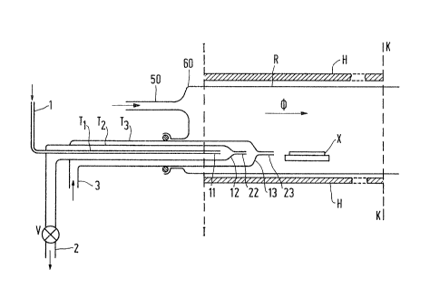
As shown in Figure 1, the arrangement used in the method
of ~anufactuxing a semiconductor device according to the invention
co~prises a system of three coaxial tubes T1, T2, T3.
The first tube T1 (the inner tube) has a diameter
smaller than that of the second tube T2 (the intermediate tube). This
second tube T2 has in turn a dia~eter smaller than that of the third
tube T3 (the outer tube).
The ends 1, 2 and 3 (the first ends of the three tubes
30 T1I T2, T3) are independent. The three tubes T1, T2, T3
become integral and coaxial only in the proximity of their second ends
11, 12, 13.
The second end 11 of the inner tube T1 ~erges into the
intermediate tube T2 in the proximity of the second end 12 of the
latter.
The second end 12 of the intermediate tube T2 is
provided with a restriction 22 and merges into the outer tube T3 in
PHF 86547 5 21.0~.1987
the proxi~ity of the second end 13 of the latter.
The second end 13 of the outer tube T3 is provided with
a restriction 23 and merges into the chamber of the reactor R.
The first end 2 of the intermediate tube T2 is provided
with a valve V.
The chamber of the reactox R co~prises a space in which a
monocrystalline semiconductor sample X is placed on a sample carrier.
Tbe sa~ple carrier is arranged in the proximity vf a source of heat
situated outside the chamber so that the sample is situated in a hot
zone whose temperature is that required for the epitaxial growth from
the vapour phase.
The compounds necessary ior the epitaxial growth o a
layer or reactants are introduced in gaseous for~ and form a flux
~ which circulates from one end 60 of the chamber in the
direction of an outlet to the other end of the chamber and which passes
into the hot zone of the chamber in the direction indicated by the arrow
in Figure 1.
The reactant gases ~ay be either products entering the
composition of the epitaxial layer itself or products intended for
~0 doping of said layer. These reactant gases are mixed with a gas which is
neutral for the reactor (the so-called v0ctor gas) and their partial
pressure with respect to this neutral gas has to be determined with a
high accuracy.
As has been stated above, certain of these reactant gases
have the disadvantage of being stronqly adsorbed by the cold walls.
These ~ases must then necessarily be introduced into the hot zone of the
reactor bounded by the planes whose countour is II and KK in Figure 1.
According to the invention, the reactant gas is
introduced through the end 1 of the inner tube T1 and circulates in
the direction of the second end 11 to the intermediate tube T2.
The vector gas is introduced through the end 3 of the
outer tube T3 and circulates in the direction of its second end 13 to
the cha~ber of the reactor R.
As shown in Figure 2, which represents the equivalent
circuit diagram oE the system, when the valve V is closed, the system
behaves like a com~utation valve which directs the whole quantity of
reactant gas to the chamber R.
6 2010~-8304
When on the contrary the valve V ls opened, the system
behaves like a commutation valve which directs the whole guantity
of reactant gas to the first end 2 of the intermedlate tube T2,
the flow rate of the vector ~as being much higher than the flow
rate of the reactant yas (of the order of 5 to 10 times higher).
The system according to the invention conseyuently
provides the advantage mentioned above and more particularly the
advantage that it takes along the reactan~ gases to the
intermediate proximity of the hot zone, as shown in Figure 1,
which permi~s of avoiding the adsorption and desorp~ion phenomena
after commutation and hence of avoiding the disadvantage of ~he
memory effect.
On the other hand, there can be provided in the chamber
of the reac~or R in the proximity of the area 23 at which the tube
T3 merges an inlet 50 for gaseous compounds less sensitive to the
cold walls cixculating to the outlet of the chamber R in the same
direction as the reactant gas and the first vector gas.
Theæe compounds can be supplied by a device of the kind
described ln U.S. Patent 4,722,911 issued February 2, 1988. This
Patent discloses a device which permits of very accurately
controlllng the partial pressures of each of the reactant gases
leading to the realization of epitaxial layers from the gaseous
phase whose composition and khickness are very precise.
Finally, there can be provided in the chamber of the
reactor at the end 60 of the latter one or several other devices
accordiny to the present invention for different reactant gases.
~ An example o~ a reactant gas which is strongly adsorbed
by the cold walls and at the same time is frequently used in the
2~
6a 20104-8304
manufacture of the semiconductor devices for doping of the layers
especially of galllum arsenide (GaAs) is selenium hydride (H2Se).
It will be clear that the tube system accordiny to the invention
is particularly favourable for the formation o~ epitaxial layers
doped with selenium (Se).
A very favourable material for realization of the tube
system according to the invention is quartz because this material
is particularly easy to decontaminate in the application for the
manufacture of semiconductor dev1ces, for example of the group
III-V. Moreover, quartz satlsfies all the purity conditions
sultable for
PHF 86547 7 21.04.1g87
formation ~f epitaxial layers of high quality.
It should be noted that the operation of the tuhe system
according to the invention does not depend upon the high quality of the
valve V ~cf. Figure 1). In fact, this valve may, for example, leak
slightly without the operation of the system being adversely affected
thereby. This guarantees a long life for the system according to the
invention.