Note: Descriptions are shown in the official language in which they were submitted.
--2--
,Background Art
Photovoltaic solar cells are semiconductor
devices ~hich convert sunlight into electricity. Cur-
rent applications rely largely on single crystal sili-
con solar cells. Such solar cells have proven to be
too costly for general commercial use. The principal
reasons for this hig~ cost are the expense of single
crystal silicon, the cost of forming this single crys-
tal (or large grain polycrystalline) silicon into
sheets and the absence of high throughput continuous
manufacturing processes.
Significant cost reductions can be achieved
by using thin-film solar cells. Thin-film solar cells
are made by depositing or growing thin films of semi-
conductors on low cost substrates. These thin-film
devices can be designed to reduce consumption of semi-
conductor material by more than 80~. Design require-
ments for thin-film cells are provided by A. M.
Barnett, et al., ~Thin Film Solar Cells: A ~nified
Analysis of Their Potential,~ IEEE Tra~sactions on
Electron Devices, Volume ED-27, Number 4, April 1980
2~ pages 615 to 630.
Development of thin-film solar cells has
been inhibited by problems relating to micro- and
macro-scopic defects and to fabrication techniques.
~2~
Thin-film ~olar cells are generally polycrystalline ln
nature. That i5, the sem~conductor layer6 are com-
prised of small crystallites. Where crystallites ad-
joint there are cry~tallographic lmperfectlons, known
in the art as grain boundaries. Grain boundaries pos-
sess properties which are different fro~ bulk cry~tal
properties, including their electrical and chemical
properties, Grain boundarie~ are kno~n to be the
cause of shunts and shorting effects which degrade
open circuit voltage and fill factor, recombination
which degrades short circuit current, and interdiffu-
~ion which degrades reliability and stability.
Another problem confronting the development
of thin-film Eolar cells using polycrystalline semi-
conductors is the occurrence of macroscopic defects
such as pin-holes, -voids and cracks. An electrical
short occurswhen there is a pin-hole in the semicon-
ductor layers of the solar cell and the front and b~ck
electrical contacts to~ch. Such macroscopic defect~
severely~limit performance and manufacturing yield.
Still another problem is the fabrication of
thin-film solar cells. Thin-film ~olar cells are made
by sequentially gro~ing the 6emiconductor layers over
a substrate which includes electrical contact means
and, for ~ome solar cell designs, optimized light
tranEmiSSiOn and reflection features. Effective meth-
ods of gro~ing semiconductor thin-films on substrates
have been limlted by contamination of the 6emiconduc-
tor gro~th environment by the substrate, lnterdiffu~
~ion and chemlcal reaction between the substrate and
emiconductor during growth, degradation of substrate
electrical and optical properties during gro~th, the
inability to control nucleation and grain size of the
semiconductor layers, and shunts and shorts caused by
the grain boundariefi.
Solutions to some of the aforementioned
problems are known in the photovoltaic art. One solu-
tion to ~acroscopic defects, described in u.s. Patent
~o. 4,251,286 issued February 17, 1981 to A. M.
Barnett, is selectively forming an insulator or appro-
priate semiconductor material which effectively blocks
shorts and shunts that are caused by macroscopic de-
fects in the semiconductor layers of thin-film solar
cells.
D. E. Carlson, et al. indicate in United
States Department of Energy Report No. SAN 1286-8,
entitled ~morphous Silicon Solar Cells, Final Report
For The Period 1 July 1976 to 30 September 1978 Under
Contract No. EY-76-C-03-1286~, October 1978, pp. 22-
24, that electrical ~horts can be eli~inated by the
use of resistive films having a thickness equal to or
greater than that of the ~emiconducting fil~ m e
Report describes alleviating the problem of shorts due
~2t~
-5-
to p~n-holes by use of a thick back-cermet ball~st
resistor such as Ni-SiO2.
Solutions to microscopic defects associated
with grain boundaries include selectively depositing
an insulating cap at the surface intersection of the
grain boundaries, described in ~.S. Patent No.
4,197,141 iss~ed April 8, 1980 to C. O. Bozler, et al.
Bowever, this approach does not eliminate the adverse
effects of grain boundaries within the semiconductor
layers. ~.5. Patent No. 4,366,338 issued December 28,
1982 to G. w. Turner, et al. describes electrically
passivating grain boundaries in p-type GaAs by intro-
ducing tin as an n-type compensating dopant into the
intersticies of p-type grain boundaries. ~owever, the
grain boundary passivation approach of Turner, et al.
has not proven to be effective.
Solar cells which are deposited on a sub-
strate are described in ~.S. Patent 3,914,856 issued
October 28, 1975 to P~~. Fang. Patent No. 3,914,856
teaches evaporating an aluminum metal contact elec-
trode on a fle~ible ubstrate and depositing a thin
layer of crystalline silicon. According to the pat-
ent, the aluminum substrate is used for a nucleation
site for growth of the silicon crystals and for auto-
doping of the silicon. Such a solar cell embodies all
of the aforementioned disadvantages that have inhib-
ited development of thin-film solar cells. Patent No.
--6--
3,914,856 also mentionE; lntroducing ~ 6illcon oxide
lsyer to the substrate before the metallic electrode
evaporation as an additional step. The ~ilicon oxide
1 ayer is described as serv ing three purpose~: el ec -
trical insulation from the substrate; redl~ction of
diffusion between the substrate material and the semi-
cond~ctor; and better matching of the substrate for
qrowing sil icon films.
I~.S. Patent No. 3,961,997 issued June 8,
1976 to T. L. Chu describes preparation of polycrys-
talline silicon solar cells by depositing successive
1 ayers of doped ~ilicon on steel substrates which are
coated with a diffusion barrier of sil ica, borosil i-
cate or phosphosilicate.
A probl em inherent in the sol ar cell s of the
Patent Nos. 3,914,856 and 3,961,997 is that layer~ of
silica, silicon oxide, etc., are electrical -insula-
tors. Patent No. 3,914,856 does not describe electri-
cal contact means in such sol ar cel 1 s. Patent No.
3,961,997 describes placing ohnic contacts in the n-
and p- regions of the dev ice on the 1 ight receiving
top surface of the silicon. Thin-film solar cell~
with both electrical contacts on the front rurface of
the silicon have the disadvantages of increased co~;t
and unacceptabl e losses in performance.
Some of these problems associated with
growth of thin-film semiconductor~ on 6ubstrates can
be overcome by the metallurgical barrier layers des-
cribed in European Patent Office Publ~cation No. 0 079
790, dated May 25, 1963, for E~ropean Patent Applica-
tion ~o. 82306066.0 of A. M. Barnett. The EPO publi-
cation describes barrier layers, such as 6il icon car-
bide or tin oxide. Such barrier layers ~erve several
useful functions: prevent contamination and dlffusion
during semiconductor growth; electric~l communication
between the substrate and semiconductor layers; and
enhanced optical reflection for increased efficiency.
Rowever, metallurgical barrier layers do not overcome
problems associated with macroscopic oefects or micro-
scopic defects such as arain boundaries.
Applicant has recognized that these obsta-
cles to developing high efficiency, low cost thin-film
solar cells can be surmounted by providing an improved
substrate for thin-film solar cells. Accordingly, an
object of this invention is to provide a solar cell
which includes a novel substrate having an insulator
and electrically conductive nucleation sites. Another
object of this invention is to provide methods for
making improved thin-film solar cells which include
fabrication of a novel ~ubstrate.
Su~a~y of the Invention
~ thin-film solar cell comprises semiconduc-
tor layers formed on a substrate. The substrate in-
clu~es an electrical contact and an insulator contain-
ing a plurality o electrically conducting nucleation
sites. Microscopic and macroscopic defects which
penetrate the semiconductor layers terminate on the
insulator which ~s interpo~ed between the electrical
contact of the substrate and the adjacent semiconduc-
tor. The semiconductor layer~ communicate electrical-
ly with the electrical contact of the ~ubstrate
through electrically conducting nucleation sites in
the insulating layer. The insulatins layer prevents
contamination of the semiconductor 12yers and growth
environment during growth of the se~iconductor layers.
The nucleation sites are located in the insulating
layer such that electrical resistance and grain boun-
dar~ losses are minimized.
The thin-film solar cell is fabricated in a
process which comprises ~electively introducing nu-
cleation sites into the substrate material, forming an
insulator layer and activating the nucleation sites
during growth of the semiconductor layers. Alterna-
tively, the process comprises selectively introducing
nucleation sites into the insulator ~aterial, ~pplyin~
the insulator containing nucleation sites over the
electrically conducting plane of the 6ub~trate and
then forming the semiconductor layer~.
The Dra~in~s
Fig. 1 is a cross-~ectional view, enlarged
and not to scale, illustrating macroscopic and micro-
scopic defect~ in thin-film solar cells known in the
art.
Fig. 2 is a cross-sectional vi~, enlarged
and not to scale, of a thin-film solar cell having a
substrate in accordance with this invention.
Fig. 3 is a diagram illustrating the steps
for making a substrate and including cross-sectional
view~, enlarged and not to scale, of the substrate in
accordance with this invention.
Detailed Description
Fig. 1 illustrates a thin-film solar cell
10. m e solar cell is formed on substrate 10~. Sub-
strate 100 includes ~upport member 110 and first elec-
trical contact 105, which is a continuous electrically
12~2~16
--10--
conductive layer. Support 110 and contact 105 can be
of the same material ~uch as a sheet of Gteel or
aluminum, in which case support 110 provides electri-
cal contact means for operation of the solar cell.
Fir~t semiconductor layer 130 is in ohmic contact with
electrical contact 105. Second ~emiconductor layer
140 is of oppo~ite conductivity type to layer 130 and
rectifying junction 135 is formed between ~emiconduc-
tor layers 130 and 140. Second electrical contact 150
makes ohmic contact to layer 140. When sub~trate 100
is opaque to liyht, contact 150 is essentially trans-
parent in the form of a grid and light enters the
solar cell through layer 140. When substrate 100 is
transparent to light, contact 150 maS~ be opaque and
light enters the solar cell through layer 130. Semi-
conductor layer~ 130 and 140 may be of the ~ame
material, as in homojunction solar cells, or of dif-
ferent materials, as in heterojunction solar cells.
When semiconductor layers 130 and 140 are
polycrystalline thin films, there occur microscopic
defects, such as grain boundaries 160, and macroscopic
defects 180, which extend through semiconductor layer6
130 and 140. Certain grain boundaries 160 are low
resi~tance electrical paths. When at least one of the
electrical contacts, 105 or 150, is continuous, elec-
trical flow along grain boundaries can effectively
shunt the ~olar cell. This leads to reduced open
circuit voltage and fill factor. Furthermore, since
12~i24~3~
nucleation of 6emiconductor layer 130 on cont~ct layer
105 i6 es6entially random, there are many clo6ely
spaced grain boundaries in semiconductor layer 130
which can act as recombination centers and reduce the
output of the solar cell. Macroscopic defects 180
give rise to 6hort circuits when second electrical
contact lS0 touches first electrical contact 105.
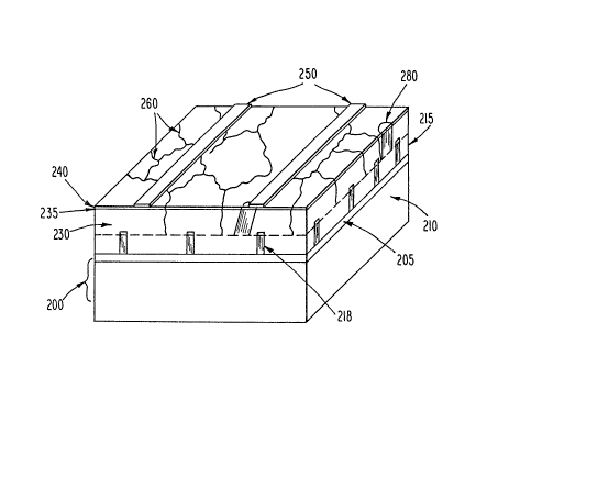
Fiy. 2 ill~strates a thin-film solar cell 20
which includes an improved substrate 200 in accordance
with this invention. Sub6trate 200 compri6e6 support
meTnber 210, electrical corltact layer 205 and in6ulator
215. Contact layer 205 may be omitted, in which case
~upport 210 provides electrical contact means for
operation of the ~olar cell. Insulator 215 contain6
electrically conducting nucleation sites 218. ~n
accordance with this invention, grains of first 6emi-
conductor layer 230 grow preferentially from nuclea-
tion sites 218. By ~electing the di6tribution and
spacing between nucleation 6ite6 218, the problems of
random nucleation and control of grain size are over-
come. There are also contained in insulator 215 a
certain number of 6ites (not 6hown in Fig. 2) which
are not active. The not active nucleation sites (non-
active) are e6sentially insulative or are substant~al-
ly less conductive than active ~ites.
~2~
-12-
The grains meet at grain boundaries 260
which term~nate at insulator 215. Sites 218 are
therefore located near the middle of each grain and
are located away from grain boundaries. Each grain
communicates electrically with contact 205 through
nucleation sites 21~. Second semiconductor layer 240,
which is of opposite conductivity type to that of
first ~emiconductor layer 230, i~ formed over semicon-
ductor layer 230 to create junction 235.
Semiconductor layers 230 and 240 can be p-
type and n-type 5il icon or ~-type and p-type gal 1 ium
arsenide so that j~nction 235 is a homojunction. A
heterojunction is formed when layer 230 is gallium
ar6enide and layer 240 is an oppositely doped alloy of
gallium aluminum arsenide or gallium arsenide phos-
phide. A heterojun~tion is also formed when one of
the ~emiconductor layers is an n-type ~emiconductor,
` such as c2dmium sulfide or zinc cadmium sulfide, and
2~ the other semiconductor layer is a p-type semiconduc-
~or cuch as cuprous sulfide, copper indium diselenide
or cadmium telluride. ~omojunction and heterojunction
solar cells utilizing these ~emiconductors are well
known in the art and polylcrystalline solar cell6
compri6ing them are contemplated by this invention.
-
Second electrical contact 2~0 is placed inohmic contact with ~emiconductor layer 240 to complete
the exemplary solar cell. Anti-reflection coatings,
~2~2~
-13-
electrical connectlng means and encapsulation (all not
shown) that are known ~n the art may also be provided.
Since grain boundaries 260 in ~olar cell 20
terminate on insulator 215, the shunting and shorting
effects of grain boundaries are effectively eliminated
so that the open circuit voltage and fill factor of
solar cells made in accordance with this invention are
increa~e~ Macroscopic defects 280, which extend
through ~emicond~ctor layers 230 and 240, terminate on
insulator 215 or on non-active nucleation sites which
are essentially insulative. Accordingly, short cir-
cuits between contacts 250 and 205 are eliminated in
solar cells of this invention.
Substrate support 210 may be an electrically
conducting metal, alloy, mixture, semi-metal, ~emicon-
ductor material or graphite. Metals in the form of
thin sheets are preferred. Electrical contact layer
205 is provided by one surface of conductive ~ubstrate
210 or by an electrically conductive material, uch as
a metal, alloy, mixture, heavily doped semiconductor,
conductive oxide, conductive ceramic and the like,
formed thereon, and is preferably reflective to light.
Insulator 215 is located over layer 205.
-
The objects of thi~ invention are also re-
alized when support member 210 of ~ubstrate 200 is an
insulator. In this embodiment, the support member can
i~Z4B6
-14
be a polymer, ceramic or gla~s. Electrical contact
20S is an electrically conducting la~er material such
a~ a metal, alloy, mixture, conductive ceramic, heavl-
ly doped semiconductor or transparent conductive
material such as Eilicon carbide, tin oxide or indiumr
tin-oxide. Gla~s and tin-oxide are preferred for
support member 210 and electrical contact 205, respec-
tively, when an insulative support is employed.
The efficiency of solar cells in accordance
with thi~ ~nvention may be further enhanced by textur-
ing the ~ubstrate in order to provide for diffuse
reflectance as tz~ght in the aforementioned European
Patent Application. Support 210 may be provided with
a textured surface or, alternately, contact layer 205
may be textured. In general, when the support is a
metal sheet, texturing its surface is preferred when
the support is an insulator such as glass or polymer,
a textured contact layer i8 preferre~ Means for
2~ texturing the surface of metal sheets and for pro-
viding te~tured transparent conductive oxides are
known in the art.
Insulator 215 is a thermodynamically stable
2~ electrical insulator. In accordance with this inven-
~ tion, insulator 215 also functions as a barrier which
prevents diffusion and chemical reaction between the
substrate and the semiconductor layers, and contamina-
~tion of the growth environment during formation of the
4~3~
-15-
semlconductor layer~. In~lat1ve ceramic~ and glas6e6
comprising inorga~ c oxide6, ~uch as 6ilica, alumina
and aluminosilicates, and, Eimilarly, carbides, ni-
tride6, borides and mixtures thereof can be ~elected
for insulator 215 in accordance with the teachings of
this invention. Organic materials, such as polymer
material selected iTl accordance with the teaching6 of
thi~ invent~on, are al~o suitable for insulator 215.
Por increased ~olar cell efficiency, it is
preferred that in~ulatc~r 215 have the further property
of optical transparency to light of wavelengths cor-
responding to energies near the band gap of semicon-
ductor layers 230 and 240. These properties are ob-
tained when insulator 215 is an oxide of 6ilicon or
aluminum, or mixtures thereof. The thickness of in~u-
lator 215 may be 0.1 to 100 microns.
It is further desirable to select the thick-
ness of an optically transparent insulator 215 so that
it ~erves as a quarter-wave reflector. When the
thickness of insulator 215 is selected to sati6~ the
quarter-wave reflector condition, the reflectance of
light from the surface of 205 back into the ~emicon-
2S ductor layer6 of the solar cell is enhanced and the
efficiency of the ~olar cell i~ increased~ Even when
the quarter-wave reflection condition for selecting
tne thickness of insulator 215 is omitted, optical
transparency for insulator 215 provides for reflection
8~
-16-
of light from the surface of contact 205 and
contributes to enhanced efficiency. Further increases
in efficiency may be obtained in accordance with this
invention by providing insulator 215 with a textured
surface in order to provide for diffuse reflectance.
The benefits and conditions for realizing enhanced
efficiency from increased back surface reflecti~n and
diffuse reflection due to texturing are described in
the aforementioned European Patent Application.
Electrically conductive nucleation sites 218
are distributed throughout insulator 215. Sites 218
are comprised of electrically conductive particles of
metal, semi-metal or semiconductor materials.
Semiconductor materials such as silicon or germanium
are preferred. Sites 218 which comprise a
semiconductor material contain a sufficient
concentration of impurities or dopants to provide the
required electrical conductivity. For example, when
sites 218 are silicon, aluminum may be incorporated as
a dopant to impart the needed conductivity.
Sites 218 intersect the surface of insulator
215 that is adjacent semiconductor layer 230 and
provide electrical communication between the grains of
semiconductor layer 230 and electrical contact 205 of
the substrate. The cross-sectional area of sites 218
~Z~
-17-
and their distribution within insulator 215 are
selected to optimize grain size in semiconductor layer
230 and electrical resistance between the
semiconductor and the substrate.
Grain size in semiconductor layer 230 is
determined by the distance between nucleation sites.
lo The relationships between grain size and current
output of a solar cell are described in the
aforementioned IEEE Trans~Lct~Qns on Electron Devices
publication of Barnett, et al., and by A. ~. Barnett,
et al., "Design and Development of Efficient Thin-Film
Crystalline Silicon Solar Cells on Steel Substrates,~
Proceedings of the Sixth EuLs~ean Community Photovoltaic
~Ql~L Energy ~onference, D. Reidel, Boston, 1985, pp.
866-870.
The electrical resistance is determined by
the cross-sectional area of the sites, the bulk
resistivity of the site material, the spacing between
sites and the thickness of the insulator in accordance
with Ohm's law. In general, the voltage drop due to
the resistance of a site should be less than 2% of the
maximum operating voltage of the solar cell when the
solar cell is generating its maximum operating
current. Since each site collects current generated
by a single grain in layer 230, it is a straightforward
~262
--18-
matter to design the solar cell ln accordance with
this invention.
In one embodiment of thi~ invention, ~olar
cell 20 is a silicon solar cell. Substrate 200 can be
a ferrous alloy such as steel or a non-ferrous materi-
al ~uch a~ aluminu~ The aluminum 6ubstrate should
contain 5~ to 25~ ~ilicon, by weight. Alum~num and
silicon at the eutectic ratio, 87.4% aluminum and
12.6% silicon, in the form of a smooth ~heet is pre-
ferred for an embodiment of this invention wherein
nucleation ~ites are introduced ~nto the substrate.
Insulator 215 can be an oxide such as an
oxide o~ aluminum or silicon, alone or in combination,
at a thickness of 0.1 to 100 microns. Alumina having
the formula A12o3 and a thickness of 0.1 to 1 microns
is preferred for the case of the aluminum:~ilicon
substrate.
Sites 218 can be silicon or germanium. Sil-
icon doped with aluminum is preferred for sites 218.
Semiconductor layer 230 is p-type silicon 2 to 50
microns thick, preferably 10 microns thick, and ~emi-
conductor layer 240 i~ n-type silicon less than 1.0
microns thick. m e grain size in silicon semiconduc-
tor layers 230 and 240 ~hould be at least two times
the thickness as tau~ht in the aforementioned publica-
tions by Barnett, et al.
lZ~ 6
--1 9--
A GaA~ ~olar cell in accordance with thi6
invention utilizes n-type GaA~ for 6emicond~ctor 230
and p-type GaAs for emiconductor 240. P-type grain
boundaries which are present in the n-~ype layer ter-
minate on insulator 215. Each individual grain commu-
nicates electrically with conductor 205 through nu-
cleation sites 218. These nucleation sites are lo-
cated toward the middle of the grain and away from the
~rain boundary. When 601ar cell 20 i; a GaAs 6~1ar
cell in accordance with this invention, ~ilicon nu-
cleation sites are preferred. The resi6tivity of each
nucleation site i~ less than 0.1 ohm-cm, the cross-
section area is about 7x10⁻⁸ ~q.c~ and the sites are
distributed within a 0.1 to 1.0 micron thick A12O3
insulator with an average site-to-site distance of
about 10 microns.
Another GaAs 601ar cell in accordance with
thi~ invention includes an n-type GaAlAs blocking
layer interposed between insulator 215 and n-type GaAs
~emiconductor layer 230. The function of blocking
layer~ in thin-film photovoltaic solar cells is des-
cribed in aforementioned ~.S. Patent No. 4,251,286.
Grain boundaries which penetrate both layers terminate
on insulator 215. ~owever, p-type grain boundarie~
which penetrate layer 230 and terminate on the n-type
GaAlAs layer form a high voltage heterojunction in
parallel with the n/p GaAs homojunction BO that grain
-20-
boundary shorts are further blocked. Solar cells
utilizing GaAs in accordance with this invention may
also include a p-type GaAlAs window layer over p-type
GaAs layer 240 in order to reduce surface
recombination and to enhance the efficiency of the
solar cell. GaP or graded GaAsP can also be used for
the window layer, as taught in U.S. Patent. No.
4,582,952 issued April 15, 1986 to A. M. Barnett et
al. ~hen a GaAs solar cell in accordance with this
invention is of the type "N on P,~ wherein layer 230
is p-type and layer 240 is n-type, p-type grain
boundaries terminate in the window layer.
An essential feature of this invention is
preparation of substrates having an insulator and
electrically conducting nucleation sites~ A broad
embodiment of the invention is illustrated in Fig. 3
where the steps, 30, and cross-sectional views, 300,
of the substrate at the completion of each step are
shown. Beginning with step 32, the material of
nucleation sites 318 is introduced into the substrate
material 310 and the substrate containing nucleation
site material 318 is shaped forming intermediate
substrate 320. Optional step 34 is selectively
etching the substrate to expose the sites, yielding
intermediate substrate 340. Optional step 34 may be
accomplished by chemical etching of the metal as is
known in the art. For example, hydrochloric acid etches
;2~
-21-
aluminum without ~ignificantly etching ~illcon. Step
36 is form~ng an insulator by oxidizatlon resulting in
oxides 362 and 364 covering the substrate material and
site~, respectively, and yielding intermediate sub-
strate 360. Step 38 is activating the sites by selec-
tively removing oxide 364, thereb~ exposing nucleation
sites 318 on the surface of ~ubstrate 380 whereon the
semiconductor layers are formed. Activation of the
s~tes can take place in a separate step prior to
forming the 6emiconductor layer6. Methods for activa-
ting ~ites are chemical etching, plas~a etch~ng, and
vapor phase etching u~ing a halogen bearing gas.
Preferably, activation is acc~mplished during the ini-
tial stages of growth of the semiconduct~r layers.
For example, when growth of the semiconductor layers
is by the preferred solution growth method, a ~mall
amount of a selected chemical reducing agent added to
the growth solution will chemically reduce oxides
covering nucleation sites, but will not attack the
2D insulator. The reducing agent is preferably selected
on the basis of thermodynamics. For example, the
change in free energy resulting from reaction between
the reducing agent and the site oxide should be nega-
tive, while the free energy change for reaction be-
tween the reducing agent and the insulator should be
po~itive. Tabulated values of standard enthalpies of
formation are useful for selecting the reducing agent
in accordance with the teachings of this invention.
~owever, when thermodynamic data i5 unavailable or
36,
w},en activating the sites involves chemical reaCtiOnS
other than reduction of an oxide, experin,entation will
provide the necessary information to se~ect aaents
that are effective for activating the sites.
An example of the method of Fig. 3 in ac-
cordance with this invention includes preparing a
mixture of aluminum and silicon, melting the mixture
and casting an in~ot of the mixture in which silicon
cr~stallites are dispersed in the aluminum. ~he sili-
con crystallites function as precursors to the nuclea-
tion sites of this invention. Aluminum containing 5
to 25~ silicon may be used. An aluminum-silicon eu-
tectic having a meltina point of 577~C and a composi-
tion of 12.6~ silicon and 87.4% aluminun, is preferred
in order to obtain a narrow distribution of silicon
crystallite sizes and desirable mechanical properties
for shaping. The ingot is then shaped to a configura-
tion suitable for use as a substrate, preferably by
rolling, to form thin sheets. The electrical conduc-
tivity of the silicon sites, required b~ the teachings
of this invention, is provided by the doping effect of
aluminum.
The substrate is then exposed to oxygen at
temperatures of 200 to 400C for a period of 2 to 20
minutes, forming A12o3 insulator over the substrate
and SiO2 over the sites by thermal oxidation. The
oxidation is carried out to an extent sufficient to
~ 4~ ~
provide a thickness of insulator in accord with the
teachings of this invention. Alternatively, the
oxidation may be accomplished by electrolytic
anodization or by exposure to an oxygen containing
plasma. Thermal oxidation in dry oxygen at a
temperature of 300C for 10 minutes is preferred.
Silicon semiconductor layers are preferably
deposited by the solution growth method, described in
the aforementioned European Patent Application,
whe~eby silicon is deposited from a saturated solution
in molten tin in the presence of a temperature
gradient. For the selected reducing agent of this
invention, 1% aluminum is added to the growth
solution. Magnesium, though less preferred, may also
be used as the reducing agent. Contact between the
substrate and the molten tin containing aluminum
selectively removes the SiO2, thereby exposing and
activating the sites. Once the sites are thus
activated, crystallites of silicon grow to form the
semiconductor layers of the solar cell of this
invention.
The preferred method of solution growth in
accordance with this invention may also be practiced
USill9 a variety of solvents which were known in the
art. D. Rass et al. in a publication entitled "Liquid
Phase Epitaxy of Silicon: Potentialities and Prospectsn,
Physica, Vol, 129B, pp. 161-165 (1985), describe use of
~2~
-24-
Ga, In, Sn, Bi and alloys of these elements with
dopants s~ch as P or As. Other solvents such as lead
or germanium, and other dopants such as Sb, In, Al or
Ga may also be used for growing the sen,iconductor
layers.
Alternate methods of forming the semicond~c-
tor layers to fabricate solar cells according to this
invention include chemical vapor deposition, plasma
assisted chemical vapor deposition, vacuum evapora-
tion, sp~ttering, electrodeposition and spray pyroly-
sis, all of which are well kn~wn in the thin-film
semiconductor and photovoltaic arts. ~he layers may
be re-crystal1ized in order to enhance crain size.
Solar cells utilizing GaAs in accord with
this invention can also be fabricated using the method
of Fig. 3 whereby an aluminum-silicon substrate in-
cludes an aluminum oxide insulator containing silicon
sites. h~hen the GaAs semiconductor layer is grown
from a saturated solution in molted Ga, activation of
the sites occurs by contact with molten gallium con-
taining 1~ aluminum.
A second method for fabricating solar cells
irl accordance with this invention comprises selective-
ly introducing nucleation site material into an insu-
lator material, applying the insulator containing
site material over the electrical contact layer of the sub-
4i36
-25-
strate member, activating the sites and forming the
semiconductor layers thereon. For exa~le, an insula-
tor containing introduced sites can be prepared and
applied using the methods of thick filni hybrid circuit
art. Solid particles f ~12~3~ SiO2 and other oxides
selected in accordance with the teachings of this
invention may be used alone or in combination to form
the insulator material.
1~ ~or the site material, silicon or germanium
or precursors such as oxides of silicon or germanium
may be used. The insulator and site materials are
thoroughly mixed with a liquid vehicle, such as amyl
acetate, and other agents known in the thick film art
to form a suspension or paste. The pa~te is applied
to the substrate using screen printing, doctor bla-
ding, roller coatingt spraying or like techniques.
The coated substrate is dried and fired whereby a
dense adherent layer of insulator containing sites is
formed on the substrate. Electrical continuity be-
tween nucleation sites and the conducting plane of the
substrate is established either during the firing step
or during growth of the semiconductor layers. Activa-
tion of the EiteS and semiconductor gro~th in accor
dance with this invention are as described above.
-
Insulator containing sites can also be ap-
plied to the substrate using the methods of plasma or
flame spraying, sputtering, vacuum evaporation, chemi-
-26-
cal vapor deposition and the like as are known in the
art of depositing composite materials and cermets.
The method of applying an insulator already
containing sites is particularly suited to fabricating
a solar cell on stainless steel or glass substrates in
accordance ~ith this invention. ~or example, a chrome
steel sheet (Alloy 27) is provided with a silica
alumina glass insulator containing nucleation sites by
mixing them in amyl acetate liquid vehicle, spraying
and firing near the softening point of the composite
glass. The sites are activated during growth of the
semiconductor layers by the solution gro~th method
when 1~ aluminum is added to the tin or other suitable
solvent. When glass is used instead of steel, a
transparent conductive coating, such as tin oxide, is
applied prior to applying the insulator containing
sites material.
Electronic and opto-electronic devices which
comprise thin-film semiconductor materials formed on
substrates are also contemplated by this invention.
For example, improved light emitting diodes, photo-
detectors, thin-film transistors and the like may be
fabricated by forming semiconductor layers on an insu-
lator containing electrically conductive nucleation
sites.