Note: Descriptions are shown in the official language in which they were submitted.
2~ 7
SILICON IMPL~TT DEVICES
This invention relates to silicon devices for implanting into
animals including humans.
Various devices have been used for implants. ~or example heart
pacemakers are used to maintain an adequate heart beat rate in
humans. These can be self contained and are implanted under a
surgical operation in the chest cavity where they remain until
replaced after months or years.
Probes carrying devices have been temporarily inserted into animals
to monitor temperature etc. These are short term uses and
intrusive.
Small spheres have been injected into the blood stream and their
progress monitored. For example 10 to 25,um diameter spheres have
been labelled with a radio nuclide and their movement used in
cnecking blood flow. Such spheres are passive and can only move
with blood flow and in some cases slowly release chemicals by
dissolving.
Lyposomes, almost invariably submicron in size and incorporating
drugs have been employed therapeutically notably in the treatment
of leishmaniasis. ~gain, these devices are wholly passive.
- 1 -
,~ ,
, ~, '' ; ,:
,
' :
'
.
~i2~
-- 2 --
These problems are overcome in the present invention by using very
- small discrete active devices which are injected into the blood
circulation to collectively perform a required function such as
drug release or temperature monitoring. As an alternative to
injection direct into blood vessels the devices may be inhaled and
absorbed into the lungs for circulation within the vascular
system,or injected into joints, the cerebral ventricles, and the
urinary and genital tracts.
According to this invention a medical implant comprises
a small silicon device, less than 500 /um, capable of ~assing
along blood vessels or inhalation into lungs,
and carrying signal processing means for providin~ an output
in reponse to an input signal.
For circulation in the blood system the device are preferably less
than 7 Jum e.g. < 3 ym. For limited circulation within the large
blood vessels the device may be 250 ,um or more depending upon where
the devices are injected.
The input signal may be acoustic, electromagnetic, temperature,
nuclear radiation, p}l, or chemical.
The output signal may be acoustic, electromagnetic, explosive, or
chemical.
Energy to operate the device may be from a battery on the device or
external such as acoustic or electromagnetic in co-operation with
piezoelectric material or aerial on the chip.
3o
,
': .,
, ' ~ ' ; ' ' ` : :
'7
-- 3 --
The invention will now be described, by way of example only, Nith
reference to the accompanying drawings of which:-
Figure l is a sectional view of a device for carrying a
chemical to be released on receipt of an acoustic signal;
Figure 2 is a circuit diagram for the device of Figure 1;
Figures 3.l to 3.4 are sectional view3 showing the processing
steps in the production of the device of Figure l;
Figure 4 is a sectional view of an alternative device for
carrying a chemical to be released on receipt of an
acoustic signal;
Figure 5 is an alternative form of the device of Figure l;
Figure 6 is a circuit diagram for the device of Figure 5;
Figures 7.1 to 7.4 are sectional views showing the processing
steps in the production of the device of Figure 5;
Figure 8 i9 an alternative to Figure 5;
Figure 9 is a ~ectional view of a device carrying a chemical 7
with a self contained battery and signal processing
circuit;
Figure lO is a circuit diagram for the device of Figure 9;
Figures 11.1 to 11.8 are sectional views showing processing
steps to the production of Figure 9;
Figure 12.1 to 12.3 are sectional views showing altern~tive
processing steps;
Figure 13 is a graph of current against voltage for an FET;
Figure 14 is an alternative form of the device of Figure 9;
Figure 15 is a circuit diagram of Figure 14;
Figure 16 is a circuit diagram for a temperature-current
sensor;
Figure 17 is a circuit diagram for a temperature-voltage
sensor; and
Figure 18 is a circuit diagram for a device carrying a
chemical to be released on receipt of ionising radiation.
Figures 19, 20 are circuit diagrams for devices larger than
those of Figure 1~ for lodging in selected organs.
~5
.
.
~..
" ' : ; . ,: ,
. .
~L2~ 7
~ 4 ~
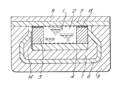
The device 1 of Figure 1 comprises a closed chamber carrying a
chemical 2. This chamber is formed by walls 3 of SiO , a bottom
p-t Si plate 4 and a top n-type Si plate 5. A layer 6 of Ti makes
electrical contact with the n top plate 5 and encloses a layer 7 of
piezo electric material e.g. ZnO. The Ti layer 6 is surrounded by
a passivating layer 8 of SiO whilst the n top plate 5 i8 covered
by a p+ Si layer 9. A cermet resistor 14 connects the p~ ~i plate
and the titanium plate of the piezo e:Lectric material 7.
As seen in Figure 2 the chemical is held between conducting
plates 4 and 5. An a/c voltage is generated in the piezo electric
7 when it is illuminated by an acoustic beam. The output
impedance of the piezo electric is capacitive so in order to
provide a source 10 which can pass a net current a resistance 21
corresponding to the conducting path 14 is placed in parallel with
the piezoelectric material 7. The junction between Ti layer 6 and
n top plate 5 forms a rectifying diode 11 ~hich passes a d.c.
electric current through the chemical 2. This electrolyses the
chemical 2 causing gas to be generated which ruptures the cell top
plate 5, 9 allowing the chemical to escape.
In view of the small size of the devices the illuminating
ultrasound beam must be of very high intensi-ty in order to generate
an adequate voltage. In order to achieve this without heating the
tissue too much or producing streaming or cavitation effects the
ultrasound consists of very short (e.g. 5 ~s) pulses of very high
int~nsity sound r~peated at reeular intervals (e.g. 10 ms).
~ _ 4 _
, ~ .
''~
, :
:~ '' ` ', . ' . .: :
-.,~
. , :
. . : , :
. .
~2~j~8'~7
-- 5 --
For treatment in the body of a human about 10 of the Figure 1
devices are mixed into about 10cc of a saline solution and injected
into a suitable blood vessel. The blood flow causes the devices
to be carried along with the blood corpuscles. When they reach the
desired place in the body they are illuminated by a beam of
acoustic energy eg at 2.10 Hz. This causes release of the
chemical at a highly localised position in the body. The blood
flow may be normal, and go right rounci the body or blood containing
the particles may be artificially circulated round specific organs
or regions of the body. The latter approach requires surgery but
has the advantage that the flow can then avoid the lung, liver and
spleen where significant trapping occurs.
Alternatively the devices can be diluted into a carrier gas, such
as a fluorinated hydrocarbon of chain length of typically 11 or l2
(obtainable from I.C.I. Ltd., England), and inhaled. Provided the
devices are within the range < tOum they will remain in the lung
for absorption into the blood vessels. Larger devices e.g. up to
300 um can also be inhaled into the lungs.
Enhanced positioning of the devices can be achieved when treating
tumours. In this case the devices are coated with an antibody
tailored to attach itself to the tumour site only. Antibodies are
prepared from cultured samples of the tumour. Examples are
P.L.A.P. (placental alkaline phosphatase), H.M.F.G. (human milk fat
globulin), C.E.A. (Carcino Embryonic Antibody), H.C.G. (human
chorionic gonadotrophin).
-- 5 --
:.
i
:
. . . . :,
.
-- 6 --
When coated with an antibody the devices 1 readily attach
- themselves to the tumour site as they flow along the adjacent bloodvessels and capillaries. After a sufficient number have attached,
a time dependent value, they are illuminated by the acoustic beam
to release the chemical. ~y this means very high localised drug
dosages can be achieved, much higher t;han can be tolerated by the
body as a T~hole.
Coating the devices with anti-bodies may also be used for treating
against bacteria. In this case the chemical 2 carried by the
device may be gentomycin. Similarly antibody coated devices
attach themselves to bacteria and deliver very high local drug
concentrations.
The device of Figure 1 is formed by a series of steps illustrated
in Figures 3.1 to 3.4.
1. A layer 3, 1.5 um thicX of silicon oxide is grown on an n-type
Si substrate 15 of doping density < 10 cm . The oxide layer
3 i3 grown e.g. by flowing steam over a heated substrate.
~J'"~ 2. A layer 16 of photo resist e.g. Shipley AZ1470 obtainable from
Shipley Chemicals Ltd. of Herald Way, Coventry CV3 2~Q, is spun
onto the SiO layer 3 and dried. This resist 16 is exposed
through a mask using ultraviolet light. Unexposed resist is
dissolved in a developer obtainable from Shipley Chemicals ~td.
Alternatively an electron beam resist such as P.M.M.A. can be used.
After exposure with an e beam it can be developed using a 1:1
mixture of isobutyl methyl ketone and isopropyl alcohol.
;~f r~ie ~k
- 6 -
,,
1~
~ ' `''' ~ ' :
':
.' ' ': ~
~ i2 ~ ~'7
-- 7 --
3. Using the remaining resist as a mask the oxide 3 is removed
using a plasma etch. This leaves a series of holes 17 in the
oxide 3, Figure 3.1, typically 1.5 um square.
4. The remaining re~ist 16 is removed by immersion in fuming
nitric acid or an oxygen plasma and rinsing with deionised water
and dried.
5. A layer 4 of p+ Si is formed in the Si substrate 15 at the
bottom of each hole 17 for example by diffusion of boron. The
layer 4 is ty ically 0.3~m thick with a doping concentration of
2.5 . lO cm
6. A discontinuous layer 12 of Pt may be deposited e~g. by
electron beam evaporation or sputtering on the exposed p+ layer 4
in the holes 17. This Pt layer reduces the voltage subsequently
needed to operate the device.
7. The top surface of SiO is covered with a thin layer of
glue 18 for example by evaporation or printing. Suitable glues
are indium evaporated on the oxide, an epoxy resin, or rubber
adhesive printed onto the oxide.
8. An upper wafer 19 is pre~ared of n-type Si typically having a
carrier concentration of < 10 cm
: '~
: -- -: . , :- : : -
.
~ ~"
,
'7
-- 8 --
9. This upper wafer l9 has formed thereon a p+ layer 0.2ym
- thick 9 followed by an n-layer 5 of 0.2 ~m. q'hese layers 9, 5 may
be formed by vapour phase epitaxial growth using dopants o~ arsenic
for the n-layer and boron for the p-t layer.20 Ty3pical doping levels
are 5 . 10 cm for the n layer and 2 . lO cm for the
p+ layer.
10. A discontinous Pt 13 film may be deposited on the n layer.
ll. A chemical 2 is deposited in each device hole 17 by pouring a
liquid over the whole substrate and spinning or blotting off excess
chemical or squeezin& out the e~cess when the upper wafer is fixed
to the lower wafer. Possible chemicals to attack a tumour are
toxins such as nitrogen mustard, the toxin secreted by
corynebacterium diptheriae or rycin. A surfactant may be added to
help the chemical into the holes.
12. q'he upper wafer 19 is placed over the bottom substrate,
Fi&ure 3.2, with the n layer 5 in contact with the glued surface of
the oxide. Additional to or instead of glue 18 on the oxide 3
the n layer may be coated with a glue or a hardener for the glue.
Pressure is applied to seal the contactin& surfaces. When the
glue 18 is an epoxy it must be electrically conducting, e.g. by
containing metallic powder, or be removed in the area of the
chemical so that the n layer 5 makes electrical contact with the
chemica. 2.
-- 8 --
. :
~,,,
:, ~
: ,.
, ....
~2~
g
The n layer 5, oxide 3, and p+ layer 4 form closed chambers
- containing the chemical 2. One apparatus, not shown, for
pressing the upper wafer 19 onto the substrate 15 comprises a
hydraulic press. Jaws on the press are slightly curved to exert
maximum pressure at the centre of the wafer and to squeeze out
sideways excess chemical. The upper wafer 19 is placed over the
substrate 15, after holes 17 are filled with chemicals, both
placed between deformable sheets e.g. 50 ~um thick polythene, and
inserted between the press jaws. As the jaws are brought
together excess chemical is squeezed out and the layer 5 bonded
firmly to the walls 3.
13. The lower n-type substrate 15 is removed by a selective etch
such as EDA or alcoholic XDH (eq), Figure 3.2. This leaves
islands of p+ Si 4 on the SiO 3. This is described in ~.F.
Raley et al, J.Electrochem.Soc.: Solid State Science, Technolog~,
Jan 1984, 131(1) pp. 161-171; K Petersen, Proc.I.E.E.E., ~lay 1982
70(5) pp420-457; and "Thin Film Processes" edited by J. ~.
Vossen, U. ~ern, Academic Press 1978 pp 443-444.
14. Using the p~ Si islands 4 as a mask the exposed oxide is
re~oved with a plasma etch. This etching is stopped when the n
Si material 5 is reached, Figure 3.3, leaving the chamber walls 3
of oxide about 0.5 ~um thick.
, ..
: ' : ' ~ '
:. ,
''
2~
- lo -
15. Any glue 18 on the exposed n type layer 5 is removed by
- etching, e.g. oxygen plasma for an epoxy glue, or dilute
hydrochloric acid wet etch for indium glue. For an electrically
conducting glue it is advisable to etch it back under the oxida 3
to a small amount. This prevents short circuits to the chemical
from any metal layer deposited subsequently.
16. Piezo electrical material 7, e.g. ZnO , is evaporated or
sputtered onto the exposed p+ Si and oxide walls, Figure 3.3.
The ZnO i9 deposited at an angle so as not to cover the n layer
5. Since the current which electro]yses the chemical 2 mus-t pass
through the zinc oxide 7, either the zinc oxide 7 must leak or a
parallel conducting path across it must be provided e.g. by
evaporating or sputtering a thin cermet film 14. This resistance
f the film 14 must be accurately controlled since if it is too
low the piezo electric will be short circuited and if it is too
high it will impede the flow of electrolysing current excessively.
A typical resistance value is approximately 5/w.C. where w is
angular frequency of illuminating ultra sound and C is capacitance
of piezo electric layer.
17. An 0.1 ,um layer 6 of Ti is evaporated over the ZnO and
exposed oxide walls 3 and onto the n layer 5 at its junction with
the oxide 3. This is achieved by evaporating at an angle.
18. A passivating layer 8 of SiO is evaporated or sputtered
over the Ti 6 and part of the n layer 5 whilst still leaving
exposed parts of n material, Figure 3.3.
: :
19. The exposed Si, n and p+, 5, 9, is etched through to the n-
type Si 19 using the passivating oxide 8 as a mask and KOH or EDA
or a plasma as the etchant, Figure 3.4.
- 10 -
, ,,
: : .:
-: .. :~' ` ''~,
~: , ~ .'.
,. ;
~2~
20~ A wax or polymer e.g. APIEZON W~40 wax, coating 20 iS flowed
over the separate de~ices to provide support, Figure 3 ~ 4 ~
21~ The top n-type Si 19 is remo~red by a selective etch e.g. EDA
or alcoholic KOH which doe~ not etch the p+ material 9 ~ Each
device 1 is now separate and held together only by the wa~ 20.
22~ ~hen required the wax or polymer binder 20 is di3solved away
to provide unattached de~ices.
23~ If required the separate devices can be coated with an
antibody, at least on the passivating oxide.
Details of techniques for coating solid surface~ with antibodies
are contained for example in the following together with their
a~sociated reference~:-
H. H. Weetall Meth Enzymol 44 P 134
R. A. Messing Metch Enzymol 44 P 148
P. J. Halling & P. Dunnill, ~iotechnology and Bioengineering
Vol ~YI P 393~416 (1979)
In addition to direct coating of the surfaces, the surfaces can be
coated with a lipid layer to which antibodies can be attached, as
described in
TJ D. Heath, R. T. ~raley, D. Papahadjopoulos, Science 210
PP~ 539~541 (1980)
A. Huang, Y. S. Tsao, S. J. Kennel, L. Huang, 3iochem.
Biophys. Act 716, pp 140~150 (1982)
J. Barbet, P. Macky, L. D. Leserman, J. Supramolecular
Structure and Cellular Biochemistry 16 pp 243-258
(1981)~
~e~
.. `
:
~6~ 7
- 12 -
Figure 4 is an alternative form of Figure 1 using a p-n junction
rather than a Schottky barrier for the diode 11. As before a
chemical 25 is held in a chamber 26. The chamber side walls are
formed of SiO 34; the top by a p~ Si layer 27 coated with an In
glue layer 28; and the bottom by a p+ Si layer 29. A p-n
junction 30 is formed between the p+ bottom 29 and an n region 31
of Si. ZnO 32 surrounds the n region and is itself enclosed by a
Ti layer 33 which connects with the In glue 28. A cermet layer
or discontinuous metal film layer 35 is deposited to provide a
resistive link between the n-silicon and the titanium layer 33.
Processing steps are similar to that for the device of Figure 1.
~Ihen illuminated with ultrasound~ an a.c. voltage is generated in
the piezo electric which drives a current up to the indium 28,
through the chemical and the diode formed by 25, 30 and the
resistor 35. The effect of the diode is to ensure that d.c. flow
flow can only occur this way round. Hydrogen is evolved at the
p+ cathode 29 and at the anode 27 the indium glue 28 is dissolved.
The combination of these two effects lead to rupture of the cell.
The device of Figures 1 and 4 leak the electrolysing current
through the zinc oxide 7 or resistor 14. A leakage path may
instead be provided through a Schottky diode as explained with
reference to Figures 6, 7.
- 12 -
,~
.
-. ~
'7
- 13 -
As seen in Figure 5 a device 79 for releasing chemical 81 in
response to an acoustic signal comprises a closed chamber 80
formed of' a bottom plate 82, ~ilicon oxide walls 8~, and a top
plate 84. The bottom plate 82 is of n type silicon with an n~
region 85 in it3 upper surface. A thin layer 86 of Pt covers the
bottom of the chamber. The top plate 84 is p type silicon fixed
to the walls with indium glue 87. A layer 88 of piezo electric
ZnO covers the bottom plate 82 and part of the side wall 8~.
This ZnO 87 is partly enclosed by a layer of titanium 89 which
makes electrical contact with the top plate 84 and bottom plate 88
but not to the indium 87 and is itself enclosed by a passivating
layer 90 of silicon dioxide.
Figure 6 shows the circuit of the device of ~igure 5. A
generating source 91 of electricity i3 produced across the ZnO
layer 88 when illuminated by an acoustic beam. Diode Dl is
formed by Schottky contact between Ti layer 89 and top plate 84,
and diode D2 is formed between Ti layer 89 and the bottom plate
82.
~hen point A becomes negative with respect to point B current
flows through diode D2. When point A becomes positive, with
respect to B~ then current flows through the chemical 81 and diode
D1. The chemical electrolyses as before and is released from the
chamber. Since silicon will form an anodic oxide on the passage
of current in many solutions the bottom plate, which forms an
anode, is covered with the Pt layer with the heavily doped n+
layer providing a contact.
.
.. . .
.
, :
- l4 -
The device of Fjgure 5 may be formed by the following steps as
shown in ~igures 7.l to 7.4:-
l. Produce a silicon wafer 92 the bulk of which is lightly
doped, with a very heavily doped (of the order of 10 cm ) p-
type layer 93 (typically 1 micron thick) covered with a lightly
doped (about 10 cm ) n-type layer 82 typically 0.5 microns
thick. These can be produced by implanting a large does of boron
into p-type silicon 91, annealing, and growing an n-type epitaxial
layer on the p+ layer 92.
2. Deposit a layer typically 2 microns thick of silicon dioxide
83 e.g. by chemical vapour deposition, evaporation, or sputtering.
3. Deposit a 400 nm layer of polycrystalline silicon 94.
4. Photolith and etch polycrystalline silicon 94 with a plasma.
5. Grow 400A of oxide 95 on the polycrystalline silicon 94.
This will help to protect layer 94 in step 7 and densifies the
oxide 83.
o. Photolith to produce a resist mask 96 outlinin~ the devices.
7. Plas~a etch the oxide 83 down to the silicon layer 82 using
the resist mask 96. The resulting structure is shown in Figure
7.1 with spaces separating devices.
8. ~ Remove resist 96.
- 14 -
. ~ : :: :
9. Etch n type silicon 82 using the oxide 83, 95 as a mask~ going
down to the p~ layer 93. This can be done using an alkaline wet
etch such as 33~ potassium hydroxide in water or EDP which will
stop automatically when it reached the p~ layer. Alternatively a
plasma can be used, but it in this case the resist 96 must be kept
until this is done.
10. Plasma etch silicon dioxide 83 down to silicon layer 82.
using the polycrystalline silicor. 94 as a mask, see Figure 7.2.
This fo m s side walls to the chamber 80.
11. Remove the polycrystalline silicon 94 with an alkaline etch,
a plasma, or by ion beam milling.
12. Implant arsenic and anneal to produce a shallow heavily doped
n-type region 85 in the surface of the wafer 82.
13. Evaporate a layer 86 200A thick of platinum directly
downwards. This will form the lower electrolysis electrode.
14. Use angled ion beam milling to remove platinum from the top
of the oxide 83 while leaving it in the bottoms of the chambers 80.
15. The top surface of the silicon dioxide is covered with a thin
layer of glue 87 for example by evapororation or printing.
Suitable glues are indium evaporated onto the oxide, an epoxy resin
or a r~bber adhesive prlnted onto the oxide.
- 15
:
~ ' ;.; ' ~ - ' ' :
, -- ., - :.. . ~, ~.
~2~ 7
- 16 -
16. An upper waver is prepared from a p type substrate 97
carrying a 1~um thick p+ layer 98 covered by a 0.5 ~m thick p-type
layer 84. Preparation is similar to step 1.
17. A chemical 81 is deposited in each device chamber 80 and
sealed in by sticking the upper wafer down on to the lower one by
the techniques described earlier.
18. The lightly doped substrate 92 of the original wafer is
removed up to the p+ etch stop by means of an alkaline etch e.g.
EDP or a mixture of potassium hydroxide, ethanol and water.
19. ~he p+ la~er 92 is removed preferably by plasma etching. An
etch consisting of 1 part of hydrofluoric acid, 3 parts of nitric
acid and 8 parts of acetic acid, which will remove heavily doped
but not lightly doped silicon, may also be used.
20. If indium solder is used as a glue 87 it is etched back
slightly using a dilute acid.
21. Piezo electric material 88 e.g. zinc oxide i3 deposited by
evaporating onto the exposed n-type silicon 82. The deposition is
conducted at an angle so that some of the n-type silicon 82 is not
covered.
22. A metal 89 i9 deposited which makes Schottky diodes onto both
n-type and p-type silicon e.g. titanium, tungsten, nickel, or
chromium. This may be done by angled evaporation inclined to tha
opposite side to that used for step 21. This metal must make
~0 contact to both the p-type silicon 84 on top of the device and to
the n-type silicon 82 at the bottom of the device, and cover the
piezoelectric layer 880
:
- 16 -
, ~
~1
- :. ~ . ~ : .
: : ::. ,: :-
,
~ 7
- 17 -
23. A passivating layer 90 of silicon nitride, alumina or silicon
dioxide is deposited over the metal 89 and the zinc oxide 88. This
may be achieved by angled electron beam evaporation.
24. The p-type layer 2C between devices is etched through e.g. by
means of a plasma or alkaline etch similar to those described
earlier.
25. The devices are supported by a wax or polymer e.g. Aplezon
~40 wax which covers the wafer and sticks it to a rigid support
e.g. another wafer whose surface is passivated with silicon
nitride.
26. The substrate 97 is removed by a selective etch which stops
at the p+ layer 98. This may be achieved using EDP or mixtures of
water, potassium hydroxide and ethanol.
27. The p+ layer 98 is removed, either by plasma etching, or by
using a mixture of 1:~:8 hydrofluoric acid: nitric acid: acetic
acid. This separates the devices which continue to be held by the
wax.
28. The WAX or polymeric support is dissolved, releasing the
devices 79 which can be filtered out, and washed.
29. Antibody coatings can be applied i~ desired, and the devices
can be suspended m aline ior injeotion.
17
, -
: : . .,~ : : .
- 18 -
A variant on the process is to omi-t steps 25 and 26, and remove the
p+ layer 98 with the l :3:8 hydrofluoric acid:nitric acid:acetic
acid etch by etching from below and filtering ou-t the devices. In
this case it is desirable that the passivating layer 90 deposited
5 in step 23 should be of silicon nitride since it is attached much
more slowly than silicon dioxide or heavily doped silicon by the
etch. Further variants involve replacing the p+ etch stop layers
98 by silicon dioxide layers. Buried silicon dioxide layers can
be produced by high dose high energy ion implantation by
recrystallising polycrystallire silicon on top of silicon dioxide
(see S. M. Sze, VLSI Technology. McGraw Hill 1983 p 83 ff), or by
anodising a p-type layer of silicon under a surface layer of n type
material to form a buried layer of porous silicon which can be
readily oxidised to give a buried oxide layer (K. Imai, H. Unns,
I.E.E.E. Trans. Electron Devices, ED 31 (3) ~larch 1984 p 297 ff,
U.S. Patent 3,919,060 H ~ Pogge et al 1974). A general review of
methods of growing producing silicon on silicon dioxide is given by
L. Jastrzebski, J. Crystal Growth 70 (1984) p 253-170.
Figure 8 is an alternative to Figure 6. As before device 100
comprises a chamber 101 formed by a p-type silicon bottom plate
102, silicon dioxide side walls 103, and an n type sllicon top
plate 104. A ring of indium glue 105 holds the top plate 104 in
place. To avoid a Schottky barrier at the glue joint a thin n+
25 silicon layer 106 is formed on the lower surface of the top plate
104. A piezo electric layer 107 of ZnC is formed on the bottom
plate 102 and part of the side walls 103. A layer of Ti 108
covers part of the ZnO layer 107 and makes electrical contact with
the top plate 104. Contact by the layer 108 with the glue 105 is
avoided by reces~ing the glue layer 105. A passivating layer 109
of silicon dioxide covers the ZnO and Ti layers 107, 108.
- 18 -
.,
..,..,. ~ .
~ .: ' .' ~ ' :
-- 19 --
The device of Figure 8 differs from that of Figure 5 in that the
top plate 104 acts as an anode and the bottom plate 102 as a
cathode. Diodes are formed, as before, between the Ti layer 108
and bottom plate 102 and Ti layer 108 and top plate 104.
'.~J'hen a current flows gas is generated at the ca-thode 102. At the
top plate anode 104 the silicon passivates through anodic oxide
formation and the current then flows through the indium resulting
in anodic dissolution of the indium glue 105. Thi3 provide3 both
a build up of gas pre3sure and a dissolution of the indium glue.
These two effects together lead to rupture of the device and
release of chemical 110 in the chamber 101.
The proces3 for making the device of Figure 8 is similar to that
for making Figure 5 except that the lower substrate is p type and
the epitaxial layer on the upper wafer is n type with a thin n+
layer on it. In step 20 the exposed area of this n' layer is
removed e.g. with potassium hydroxide etch, so the metal 8 makes
contact to n silicon and not to the n+ layer, while the contact to
the indium is made via an n+ layer so an ohmic contact is formed
there.
- 1 9 _
~L~b`~8~ ~
~ 20 -
A self contained and self powered device 41 is shown in Figure 9
with its circuit diagram in Figure 10. It comprises a chamber 42
containing a chemical 43 such as a nitrogen mustard. The chamber
walls 44 are formed of SiO , the base 45 of p-type Si and the
top 46 of p+ Si. A layer 47 of indium holds the top to the walls.
The bulk of the base 45 is electrically isolated from the cheMical
45 by an oxide layer 40.
~elow the chamber 42 is a processing circuit formed by four FET
10 devices T1, T2, T4, T5 and a CHEi~FET T3. The transistors T4 and
T5 are not visible in the cross section shown in Figure 5. In the
bottom plate in Figure 9 are four diffused regions 48, 49, 50, 51,
with a metal strip 52 connecting the region 51 with the top plate
46. A layer of SiO forms gate insulators 53, 54, 55. Gate
15 electrodes 56, 57 are formed by deposited Al, gate 57 is also
connected to the gate of T5 and gate 56 is connected to the output
of an inverter formed by T4 and T5. A layer 58 of Si M
covers the gate elec-trodes 56, 57 and oxides 53, 54, 55, with a
hole 59 to the n+ diffusion 49. This hole 59 is covered with a
layer of refractory metal 60 forming both a conductor and diffusion
barrier. A layer of Ag 61 covers the metal 60 and gate electrodes
56, 57 to form a switch terminal 62. Since silver has a large
work function and is also connected to the most negative point in
the circuit, the silicon beneath it will tend not to invert. Thus
silver on the surface 79 can be used to supplement or avoid the
need for channel stop implants to isolate the transistors.
- 20 -
~"
" .. "
- , ~ ~., , :
" , . ' ": '' ~ ~''' .,
-: ,
~l~62~ 7
- 21 -
Above the chamber 42 is a battery 68 formed by a bottom
electrode 63 ? electrol~te 64, top electrode 65 and Ag switch
terminal 66 in serial layer order. An insulating alumina ring 67
is arranged on top of the p+ top plate 46 and extends below the
indium glue 47 onto the side walls 44.
Figure 10 shows the circuit diagram for the device of ~igure 9.
The batter~ 68 is formed by the negative electrode 65, electrolyte
64, and positive electrode 63. The Ag layer 66 forms one terminal
69 of a switch 70, with the lower Ag layer 61 forming the other
switch terminal 62. Immersion of th0 device 41 in a suitable
solution, e.g. blood, completes the circuit between the t-,ro
terminals 62, 69. '~hen ~ept under dry conditions the two terminals
62, 69 are unconnected and so the battery 68 does not run down.
Transistor T3 is formed by the n+ regions 49, 48 acting as source
and drain respectively; gate insulation is provided by the
oxide 53 and the gate electrode provided by the Al region 56.
Transistor T2 is formed by the n+ region 50 forming a source; the
n+ region 51 acts as a drain; oxide 55 forms the gate insulation;
and Al region 57 forms a gate electrode and is connected to the
source.
The CHEI~FET T1 has a source formed by n~ region 49 and drain formed
by n-~ re~ion 50; oxide 54 forms the gate insu].ation. As seen in
Figure 5 there is no gate electrode. In a CHEMFET a gate voltage
appears at the nitride surface 5~ due to the pH Yalue of the
solution in which the device is immersed. Thus the source drain
current is a measure of the pH at the nitride/solution interface.
Details of CHEMFETs are given in:-
Ion Selective Elecrodes in Analytical Chemistry Vol 2,
Editor H Freise, Plenum Press ;~ 19~0 article by J Janta
and R J Huber, P 107-173 Chemically Sensitive Field
Effect Transistors.
The device transistors T1 and T2 and T~ operate in what is termed
the sub-threshold mode. Figure 13 shows the voltage-current curve
for a field effect transistor (FET). Mormally such a device is
operated with a gate voltage above a threshold value shown as
VT. Below V the current consumption is very small but
large changes occur with voltage. Sub-threshold mode operation is
described for exanple in:-
M B Barron - "Low Level Currents in Insulated Gate Field
Effect Transistors", Solid State Electronics, Vol. 15
(1572) p.29~
R. M~ S. Sanson ~ J. D. Meingl - "Ion Implanted Complementary
MOS Transistors in Low Voltage Circuits", I.E.E.E.
Journal of Solid-state Circuits SC-7 No. 2 (1972) p.146
- 22 -
a-
,i, . . ,, ~ : -,
~., :: ,
~2~ 7
-- 2~ -
R. J. VanOverstraeten et al - "The Influenee of Surfaee
Potential Fluetuation on the Operation of the MOS
Transistor in Weak Inversion", I.E.E.E. Transaetion3 of
Electron Deviees, ED-20 No. 12 (1973) p.1t54
R. J. VanOverstraeten et al - "Inadequacy of the Classical
Theory of the MOS Transistor Operating in Weak
Inversion", I.E.E.E. Transactions on Eleetron Deviees,
ED-20 Mo. 12 (1973) p.1150
R. R. Troutman - "Subthreshold Design Consideration for
Insulated Gate Field-Effect Transistors", I.E.E.E.
Journal of Solid-State Circuits, SC-9 ~lo. 2 (1974) p.55
R. R. Troutman - "Subthreshold Slope for Insulated Gate Field-
Effect Transistors", I.E.E.E. Transaction on Eleetron
Devices (1978) p.1049
~. W. J. Barker - "Small Signal Subthreshold Model for
I.G.F.E.T.S.", Electronie Letters, Vol. 12 No. 10 (1976)
p.260
E. Vittoz & J. Fellrath - "CMOS Analog Integrated Cireuits
based on l~reak Inversion Operation", I.E.E.E. Journal of
Solid-state Circuits, SC-12 No. 3 (1977) p.224
P. Antognetti et al - "CAD Model for Threshold and
Subthreshold Conduction in MOS~ETS", I.E.E.E. Journal of
Solid-state Cireuits, SC-17 No. 3 (1982) p.454.
~ : : : :
,
-- 23 -- ~ ~
,
:: : : : :
... ,: : ~:
. - ~ :- .. .
, .. ~-. . .
- , ~ : ,
,
- 24 -
The gate voltage of a nitride pH detecting CHEMFET changes by about
55mV per pH unit. A change in 1 pH unit will therefore change the
resistance of an FET, operating in the sub-threshold mode, by a
factor of more than 3.5. This changes the voltage on the T5 gate
from about 65~ to 35p of the battery voltage. For a 3 volt
battery this is a change of 0.9 volts which is sufficient to turn
T5 on or off. Changes in pH of aboul: 0.5 units will switch T5.
T5 and T4 form an inverting switch so when T5 is turned off, the
gate voltage to T3 rises and T3 turns on.
In use about 10 devices of Figure 9 are mixed into about 10cc of
saline solution and injected into a suitable blood vessel. Normal
blood flow circulates these devices within the vascular system.
The blood pH varies within the body, around a -tu~our i-t may drop by
around 0.4 units. For a large intraperitoneal injection of
glucose this differences increases to one pH unit as described by:-
M. Eden, B. Haines, H. Kahler, J. Nat. Cancer Inst.,
16(2) p.541ff (1955~
H. Kahler, ~. V. B. Robertson, J. Nat. Cancer Inst.,
3,pp.495-501 (1943)
P. Gullin et al, J~ Nat. Cancer Inst.,
34(6) p-857 ff (1965)
S. A. Shah, R K. Jars, P. L. Finney, A. L. Yee, 35th Annual
Conference on Engineering in Medicine and Biology,
Marriott Hotel, Philadelphia, PA, 22-24 September 1982,
p.1~8.
- 24 ~
:.
! . ' .
~ .
~L~62~`7
- 25 -
When in the blood the battery is switched on since blood conducts
electricity. The battery voltage i5 divided bet~een the CH~FET
T1 and FET T2 ac-tin~ as a resistor because its gate and source are
connected together, both operate in sub-threshold mode and so
5 consume very little power. If the blood pH falls, the drain
voltage of T1 changes and comparatively large changes are produced
in the gate voltage of T5 thus turning it OFF. This causes the
gate voltage of T3 to rise turning it on.
In this condition the battery 68 is connected across the cheMical
chamber 42, i.e. between p+ plate 46 ~nd n+ region 48, so the
chemical 43 is electrolysed. The resulting gas pressure ruptures
the chamber 42 and releases the chemical 4~ into the blood at the
position of low pH.
Processing steps to produce the device of ~igure 9 are shown in
Figures 11.1 to 11.8.
1. A p-type layer 45 0.5 um thick is formed on a p+ silicon
20 subgtrate 75. The p+ substrate may extend for the ,rhole thickness
of the wafer or may itself by a thin layer on a lightly doped
wafer. Typically the p-type 45 layer has resistivity greater than
0.06 ohm cm and the p+ 75 is less than 0.01 ohm cm.
2. Clean the p-layer 45 and deposit SiO 1.5 um thick 44.
3. Use photo lithography and a plasma etch to produce chamber
walls 44, Figure 11.1. Typically the walls 44 are 0.5 /um thick
with an internal diameter of 1.5 pm.
~0
O
4. Grow a 1000 A thermal oxide layer 40.
- 25 -
.._
.
` - ,-,: . -:
. . :
'~
''' ~
: . .
. : ~ ~,,, ,:
'7
- 26 -
5. Ion beam mill or reactive beam etch ~"ith the beam incident at
an angle to make 2 holes 38, 39 in the oxide layer 40.
6. Form n+ regions 48, 51 in the base 45 by implanting
phosphorolls through the holes 38, 39. Implanting 5 x 10 cm
of phosphorus at ~0 keV allo~ls the 1000A oxide 40 to act as a mask,
Figure 11.1.
7. Evaporate a refractory metal 52, at an angle to provide a
strip 52 connecting the n+ region 51 with the top of the chamber
42, Figure 11.2. Platinum is preferred. This will also act as
an additional region of anode for electrolyising the chemical.
This is desirable since silicon tends to form an anodic oxide in
many electrolytes.
8. Coat the whole of upper side of the substrate ~!' th a
refractory non-contaminating inorganic oxide 76. One possible
support is magnesium oxide. An alternative is to deposit 1800A of
chemical vapour deposited silicon nitride followed by 250 ,um of
polycrystalline silicon. Processes for the deposition of thick
polycrystalline layers have been developed for bipolar SOI
applications (see L. Jastrzebski, J. Crystal Growth 70 ( 1984 ) p.
253-270). This oxide 76 acts as a support for subsequent
processing so a thick layer is required.
9. Etch away the p~ material 75 of the original ~qubstrate. A
suitable etchant is 1 part HF (aq.): 3 parts HNO (aq.): 8 parts
CH COOH. Thia removes p~ b~t not p-tvpe Si 45.
:
- 26 -
~ .
,, ,
, .~" ..,
: . . :
- . : :
: ~:
-: :
- ~
:~ .
'7
~ 27 -
lO. Form four n-~ regions 48a, 49, 50, 51a by implanting
phosphorus or ar~enic through a resist mask and annealing. Two of
the n+ regions 48a, 51 a connect through the p-layer 45 to the n+
regions 48, 51, inside the chamber 42. Threshold adjustment and
5 channel stop implants can also be done at this stage as required
using resist masking layers.
11. Grow a SiO layer 0.15 ,um thick 53, 54, 55.
lO 12. Remove SiO layer between separat;e deviceR.
13. ~emove the p-type Si 45 between devices to separate them,
Figure 11 . 3. This is achieved using the oxide 53, 54, 55 as a
mask and plasma etching or a chemical etch such as hydrazine water
15 or ethylene diamine pyrocatechol water.
14. Open up holes in oxide layer to form connections with the n+
regions 49, 50 Figure 7.3 for three transistors T1, T2, T3. At
the same time the silicon dioxide 40 between the devices is
20 etched through.
15. Form electrodes 56, 57 by depositing and etching a conducting
layer of Al, a refractory metal, or polysilicon, Figure 11 .3.
These electrodes form the gates of T2, T3, T4, T5 and connect the
25 source of T2 to the gates of T2 and T5 and the source of T4 to the
gates of T4 and T3.
-- 27 -
,
.~
:: . : , ::: :
, .
': '' . ~:
~2~j28~7
-- 28 --
16. Depo~it an Si N (nitride) layer 58 by a chemical vapour
- deposition (C.V.D.) or (if Al metalisation is u3ed) a plasma
assisted C.V.D. process. The nitride 58 covers the whole base of
the device and extends up to overlap the chamber walls 44,
5 Figure 11 .4.
17. Open up a hole 59 in the nitricle 58 to the n region 49 using
a resist mask and plasma etch. In this process nitride connecting
the devices is removed, Figure 11 .4.
18. Deposit a conducting refractory metal, e.g. molybdenum or
tantalum, as a diffusion barrier 60. This prevents diffusion of
~odium into the oxide 53, 54, when the device is in use.
15 19. Deposit Ag 61.
20. Etch away Ag 61 and refractory metal 60 to leave them shaped
as in Figure 11.5 with exposed nitride 58 at the gate of the
CHE~IFET T1. A suitable etchant for silver is nitric acid or
20 potassium cyanide. Alternatively ion beam milling with a resist
mask can be used.
21. Apply hydrochloric acid to form a silver chloride layer on
the silver electrode 61.
22. Coat bottom surfaces with a polymer or wax e.g. APIEZON ~140
wax 77 applied molten and allowed to cool. Preferably thi~
coating is thin (e.g. a few ~um) and serves to stick the chips to a
rigid support e.g. a silicon wafer or glass disc. This provides a
30 support for later processing steps.
- 28 -
:
.
:: ~' ~ `" . , -
: " '` ` ~ :
. . ~
.:
. : '
- 29 ~
23. Remove inorganic support'76 from the top of the devicesO A
suitable etchant for MgO is hydrochloric acid. Polycry3talline
silicon can be removed by potassium hydroxide solution or by
mixture of hydrofluoric acid, nitric acid and acetic acid. A
silicon nitride layer can be removed by a plasma or by hot
phospshoric acid. The structure is shoim in Figures 11.5, 11.6.
24. Deposit a thin e.g. 0.1 ,um layer of indium 47 onto the top of
the chamber 44 by evaporation at a shallow angle Figure 11.7.
Thiq acts as a glue for the chamber top.
25. Fill chamber 42 with the desired chemical 43. ~emove
surplus by spinning or wiping with an absorber or on fixing
chamber top as described earlier in the context of the piezo
electric powered device.
26. Place a p-type Si wafer 78 with a 0.4 ~1m p+ layer 46 and a
coating 0.05 um of In 47 onto the chamber walls 44. Pressure of
about 3 x 10 Nm and/or ultrasound e.g. at 20-60 kHz fixes
20 the wafer 77 to the chamber walls Figure 11.7. Typically the p+
layer 46 has a carrier concentration/doping level 2 x 10 cm
Figure 11.7.
27. Remove p-type Si 78 with a selective etch e.g. alcoholic KOH.
This does not remove the p+ material 46.
28. Evaporate or sputter SiO onto the p~ layer 46.
29. Using photolithography expose the p+ layer 46 over the gaps
between the devices.
29 -
. ,
~,...
''.- .. , ~, ;
.
::
, '
. .
, . . ..
~j2~7
- 30
30. Etch p+ layer 46 to separate each devicev Figure 11.8.
31. Remove SiO from p~ layer 46, e.g. by plasma etching,
thereby avoiding damaging the oxide on the sides of the devices.
32. Evaporate or sputter Si M or alumina 67 over the p~
layer and extend do1mwards onto the chamber walls 44 thus covering
the indium 47 and refractory metal 52 with an insulator.
33. Form a hole in the nitride 67 to expose the p~ layer 46
Figure 11.8 by photolithography. The nitride can be plasma
etched.
34. Form a battery bottom electrode 63 by evaporation or
~puttering. A suitable material is V 0 , or CoO or
V O /B 0 with a typical thickne~s of 0.3 ~m. 2
35. Form an electrolyte layer 64 typically 0O3 ~m thick by
evaporation or sputtering. Suitable materials are
(LiP0 ) (LiI) glass;
3 0.67 0.~3
2 0-37 2 5 0.18 (LiI)o 4~ glass, Alternatively
25 polyethylene oxide doped with lithium chlorate (PE0) LiClO
~ 4
could be applied by dip coating or spinning.
36. Form the negative electrode of the battery 65 by evaporation
30 or sputtering. Suitable materials are Li or LiIn or LiAl
typically 0.~ ~m thick. This ia followed by a refractory metal
e.g. W, Mo, Ta which can be electron beam evaporated, and which
prevent moisture from diffusing into the lithium.
.
:: :
, .
, ~ : . `~ ' , ,: :
' ~ ~`' ' ': '`'' ' : '
.
`:'
:: , :
, .
:ll2~ '7
-- 31 --
37. Deposit Ag 66 by evaporation or sputtering.
38. Expose Ag to HCl to form AgCl electrode 66.
5 39. Dissolve black wax 77 or polymer support. The devices are
now detached.
40. Wash and dry the devices and store in dry atmosphere. The
devices are then ready for mixing into a saline solution when
needed.
Figures 12.1 to 12.3 show an alternative fabrication process, which
avoids the need for supporting the devices at intermediate high
temperature stages and is suitable for devices containing circuits.
l 5 This has the following steps:-
1. Provide an Si substrate 114 with a layer of` about 0.5 ~m of
silicon 116 on silicon dioxide l l 5 . Pattern and etch the silicon
l l 5 to produce islands of silicon 116 on silicon dioxide l l 5 and
20 fabricate circuits 117, 118 in them. References to silicon on
silicon dioxide technology are given above.
2. Passivate circuits 117, 118 and protect with a layer 119 of
2000 A of evaporated silicon. Pattern this layer 119 where contact
25 holes are going to be needed.
_ ~;1 _
.,
-: :
.
:
- .
~6~
3. Deposit 2 ~m of silicon dioxide 121 by chemical vapour
deposition or evaporation or sputtering.
4~ Photolith and plasma etch the oxide 121 back to the silicon
116 thus forming chamber walls.
5. Deposit lOOOA of silicon nitride 122 by chemical vapour
deposition or sputtering and plasma etch to remove it from non-
vertical surfaces.
6. Use angled evaporation to produce contact 128 to the circuit
from the top of the silicon dioxide.
7. Produce a top wafer consisting of a 0.3 ~m p-~ (approximately
15 2 . lO cm ) layer 123 on a lightly doped 3ubstrate 124.
8. Deposit indium adhesive 125 on the top of the silicon
dioxide 121 and/or on the top wafer p+ layer 123.
20 9. Coat with chemical payload 127 and push substrate 114, 124
together as described earlier to seal in chemical 126, Figure 12.2.
10. Remove the lightly doped substrate 124 with a selective etch
which does not attack the p+ layer 123 e.g. potassium hydroxide
; ~ 25 solution.
: ~
: ~ :
~ 32 -
,: . . , . , -, - . :
~ : : , : ::
; ,, ~ :
::
~j2~ 7
- 33 -
ll. Evaporate or sputter a silicon dioxide layer over the whole
p+ layer.
12. Photolith and etch to remove the silicon dioxide over the
gaps between the devices.
1~. Etch through the p' layer 123 u~ing the oxide from step 12 as
a mas~ to separate the devices.
14. Fabricate and encapsulate a battery 127, Figure 12. 3 ~s in
steps 29-36 in the previous process.
15. Etch in hydrofluoric acid to dissolve silicon dioxide layer
116 and separate devices. I~ash and dry devices and store in a dry
atmosphere.
~
:"
~: . , ,
.: , .
i28~ 7
~ 34 -
An alternative implementation of a similar device in PMOS is
illustrated in Figures 14 and 15 and given the same reference
numerals as Figures 9, 10. As the solution becomes more acidic,
V of a CHEMFET T1 becomes more negative and turns off. This
causes a negative voltage to be applied to the gate of T3 which
conducts causing a current to flow through the chemical which
electrolyses leading to rupture of the cavity and release of the
chemical. The mode of operation is the same as tha-t of the l~OS
device of Figure 9 except that no inverter is required so two fewer
transistors (T3, T4) are needed. The construction process is
identical except that an n-type wafer and p-type implants are
needed to make the device and n+ channel stops 70 are required to
isolate the transistors. ~o oxide is needed to separate the bulk
of the silicon from the solution but qome platinum 71 needs to be
deposited on the positive electrode and patterned to provide an
electrolysing contact since a silicon contact might form an anodic
oxide. The platinum can be deposited by angled evaporation and
ion beam milling used to remove material from the upper parts and
tops of the container walls.
Devices similar to those of Figure 9 can be made to sense
temperatures and discharge their chemical when a given temperature
is reached. For example tumours are at a higher temperature than
surrounding tissue. Thus drugs can be released at a tumour site.
To measure temperature diodes may be used instead of a CHEMFET.
The reverse bias leakage of diodes exhibits very strong temperature
dependence. For example in silicon the leakage approximately
doubles for each 8 ~ rise in temperature.
~ 34 -
... :
::
. ~
' '; ' `
,.
~;2~
- 35 -
Alternatively temperature can be measured by means of the
te~perature dependence of the subthreshold conductance employing
circuits such as those illustrated in Figures 16 and 17. In the
circuit of Figure 16, the transistors T1-T4 set the gate voltage of
T5 to
N kT loge / S1 . S4 ¦
n ~
where S = width/length of the channel of a given transistor.
Nn = Ideality factor describing the subthre~hold slope of an n
channel i~lOSFET equal to
q 1 ~
T = Temperature
k = Boltzmanns constant
q = electronic charge.
The current through T5 And thus the current through T3 therefQre
rises exponentially with temperature. Since the drain and &ate of
T3 are linked, the drain voltage of T3 is therefore linearly
25 dependent on tem~erature. The transistor T6 forms a current
mirror from T3 so IT increases exponentially with temperature. In
the circuit of Figure 12, the gate voltage of T1 rises linearly
uith temperature. Transistors T3, T5, T7, T9 and Tl1 are current
mirrors. The pairs of transistors T2, T3; T49 T5, etc form
source followers, and the source voltage of each one is equaI to
its gate voltage plus a constant which varies linearly with
temperature so V is roughly half way between the rails V
out DD
and V and varies llnearly with temperature.
- 35 -
. :,: '..................... : ~ :
: ::
. .
- 36 -
As before the device may be partially coated with ar antibody or
with an enzyme. An enzyme may react with a specific substrate to
change the local pH ~Ihich may be detected by a CHEl~lFET, thus
increasing the range of materials which the same silicon structure
can respond to.
Alternatively, the device may be encapsulated in a cell, e.g. a
white cell. This may be achieved by allowing white cells to
engulf the device in vitro and to inject the resultant white cells
and devices. Since the body sees the white cells as frie~dly the
devices are not trapped.
Figure 18 is a circuit diagram for a device similar to Figure 9 but
which releases a chemical 4~ in the presence of ionising radiation.
The device includes a battery 68, diode D, capacitor C and FET T1,
T2 as before. The transistor Tl only passes a very small current.
When an ionising event e.g. the passage of an alpha or beta
particle occurs in the diode D, the current f'lows in the diode.
This raises the potential of point P, charges up the capacitor C
20 and turns T2 on. Current flows through T2 and into the chemical
which it releases by electrolyte rupture in the usual manner. The
device is used in conjunction with a radio labelled antibody.
First the targat tissue e.g. the tumour is labelled using a radio
labelled antibody. The isotope should emit alpha or beta
particles. The devices are then introduced into the bloodstream.
This allows the targets to be attacked simultaneously with both
radiation and chemical agents.
- 36
. . , , .:
'. ~ ~'' ";
.. .
,
, ~ ' .
~2~ 8~'7
~ 37 -
A further example of this invention uses devices tha-t are
comparatively long e.g. up to 500 ym. These cannot circulate
through capillaries but can pas~ along larger blood vessels. Thus
by choosing device size and point of injection into the body
devices can be carried deep into selected organs where whey will
lodge. Providing the shape is arranged not to block blood vessels
the devices may relatively safely remain in the vessels and perform
their required task. Suitable device shapes are L-shape and
cross-shape.
These larger devices can cary relatively complicated processing
circuits for sensing a required parameter, e.g. temperature or pH,
and provide an output signal for exernal detection or a slow
release of drugs on command.
An example of a circuit for use in these larger devices is shown in
Figure 19. The device is formed as an integrated device 135 in
the same manner as in Figure 1 or 14. A sensor 136 of temperature
or pH provides a variable voltage signal 137 to a voltage to
frequency converter 138 e.g. a voltage controlled oscillator.
Output 139 from this converter modulates a signal flowing throueh
an FET 140 from a transducer 141. This transducer 141 may be a
layer of piezo electric material between two electrically
conducting plates. The plate may be of dipole dimensions. When
irradiated by a sound source the transducer 141 provides a voltage
signal at the source frequenoy. A stabilised power supply 142
takes an input from the transducer 141 to power the converter 138
and sensor 136. Modulation of the signal passing through the
transducer 141 and F.E.T. 140, representing sensor output, is
detected externally e.g. by circuits similar to those used for
detecting doppler shifted radar returns. Conditions within a
patient's organ under study can therefore be monitored
continuously.
- 37 -
: :
, ... . ...
: ~ ' ' ': ' :
12~
- 38 -
The circuit of Figure 20 is similar to that of Figure 18. It has
a sensor 136, voltage to frequency converter 138 and sensor 136.
Instead of power being taken from an ex~ernal source the device
contains its own battery 143. As in Figure 17 the transducer and
F.E.T. 140 provide a modulated signal when irradiated by a sound
source.
Instead of or in addition to transmitting information the device of
Eigures 19, 20 may release drugs 144. Under the control of the
sensor 136 output or under the control of the externally applied
sound signal. Such drug release may be achieved by gas pressure
generated by electrolysis and may be over a prolonged period
continuously or intermittently.
More than one drug may be carried independently in the same device
and released together or in sequence.
The sensor 136 may be sensitive to ionising radiation e.g. X-rays
or alpha particles. Thus when an organ is irradiated by alpha
particles or X-rays a drug ~ould be released to reinforce the
radiation treatment. Alternatively the sensors 136 may be
sensitive to radio frequency signals to release drugs on command.
.
:
; ~ . . : ~ ` .
,
.
:
'7
- 39 -
~or devices such as those in ~igure 1 designed to circulate within
an animal blood circulation system it is necessary to know:-
(i) how lon~ devices stay in the blood:
(ii) how they are removed:
(iii) whether any major adverse effects are produced by the
devices.
To provide these results solid microdiscs silicon were neutron
activated, mixed into a saline solution, and injected into a pig'8
blood vessel. Blood samples were taken at regular intervals and
the radioactivity of the blood measured. This showed how long the
microdiscs stayed in the blood circulatory system. After blood
sample measurements indicated nearly all the microdiscs had been
removed from the blood the pig was killed. The radioactivity of
various tissues was measured to determine where the microdiscs had
finally lodged. Sections of tissue were prepared for histological
examination to see if there was any grouping together of microdiscs
and to determine the microvascular site of trapping.
Three experiments were performed, the design of each experiment
being largely dictated by the results of the previous one.
~iscussion prior to the first experiment had concluded that
microdiscs having a long clearance half life in blood would offer
greater clirical usefulness and that the first experiment should
assess the clearance rate and trapping sites of very small
microdiscs, smaller than red blood cells, which could reasonably be
expected to remain in circulation for long periods (hours). The
microdiscs were however large enough to be made using present day
technology, and for microelectronic drugs of their size to be
manufactured using technology expected to be available in fifteen
years time to carry a useful electronic circuit and drug payload.
All experiments were performed with polycrystalline silicon
microdi-qcs labelled with arsenic 76 (a gamma e~itter)O The discs
did not contain circuits or drug payloads.
- 39 -
`::
: ~'' ' ' ;
:
.
. . .
~ .
- : '
- 40 -
Experiment l was performed with three micron square microdiscs
which were 700nm thick. These microdiscs were cleared from the
blood extremel~ quickly following intravenous administration; the
vast majority were trapped in the lungs on either the first or
second circulation of the microdiscs. The extremely rapid
clearance was ascribed at the time to the square shape and sharp
corners of the microdi~cs.
Experiment 2 used 3 micron diameter circular microdiscs with a
lower specific activity of arsenic 76. Clearance was nearly as
rapid as with the 3 micron square microdiscs, resulting in barely
detectable levels of radioactivity in the blood at the time of the
first blood sample which was taken after 2 minutes. These
clearance rates were extremely surprising. Pulmonary capillaries
are reported to be seven to nine microns in diameter. The
high clearance rates suggest that mechanical trapping may not be
the sole mechanism responsible for the pulmonary accumulation of
microdiscs.
Experiment 3 used 1.5 micron circular microdiscs in an attempt to
reduce the rate of mechanical entraplment of the microdiscs.
Clearance rates were even higher than for the 3 micron circular
discs. Experiments were then suspended to review progress and to
identify further avenues of experiment.
- 40 -
,
.
" .:
... ..
:, :
~L2~
- 41 -
Procedure
Pigs of R ~ar~e ~Ihite strain were sedated with an air/halothane
mi~ture and aneasthetised with sodium pentobarbitone. Pigs were
tracheotomised and allowed to breathe spontaneously. The femoral
artery and vein of one leg were exposed and cannulae passed into
the abdominal aorta and inferior vena cava. The pig was placed in
a dorsal recumbent position and maintained by bolus intravenous
administration of sodium pentabarbitone as required. Table l
presents details of the specific activities of the microdiscs.
The microdiscs were suspended in 2 ml of 0.9~ saline ~y
ultrasonification. Eighty per cent of the solution was e~tracted
for experiments 1 and 2 (93~ for experiment 3) and made up to 5 ml
with 0.9~ saline. Small aliquots (either lO microlitres or 25
microlitres) were withdrawn as standards to estimate the total
activity ultimately injected into the animal and to provide a check
on the half life of the radio isotope. Arsenic 76 should be the
predominate isotope with a half life of 26.3 hours.
The microdiscs were administered intravenously over l minute with
multiple rinsing of the catheter and stock solution syringe.
Blood samples were withdrawn intra arterially at two minute
intervals for Experiments l and 2 and initially at o~e minute
intervals in Experiment 3. One millilitre of each sample of
withdrawn blood was centrifuged and radio activity measured in a
~ilj Model 2001 Gamma Counter. At the end of the blood sampling
period the animal was killed by exsangrination whilst still under
the influence of anaesthetic and then subjected to a post mortem
examination. Samples of tissues of 0.5-l gramme were taken,
weighed and the radioactivity measured. A total of 15 samples
were taken for Experiment 1, 22 for Experiment 2 and 60 for
E~periment 3. Further samples of lung were taken for hi~tological
examination to assess the site of trapping and whether
agglomeration of the microspheres had occurred. All measured
radio activities of the standards, blood and tissue samples were
corrected for decay to a common time.
- 41 -
.
:
::
.: .
': :,
~L2~
-- 42 ~-
Results
The entrapment of the microdiscs was so efficient for the 3.0
micron square and circular discs that the measured activity within
the blood was barely above background even though 720,C00 cps and
300,000 cps respectively had been administered intravenously (Table
1). Table 2 shows measured activities expressed as cps/ml whole
blood for these discs. In the light of these observations the 1.5
micron microdiscs were prepared with a substantially greater
arsenic 76 activity and were administered into a pig of lower body
mass (Table 1). Significant entrapment of the 1.5 micron
particles in the first minute still occurred (Table 2) but measured
activities in the blood still showed a three fold increase above
background, even after 60 minutes.
Table 4 shows isotope activity in the blood expressed as a fraction
of projected blood activity assuming instantaneous and uniform
mixing of the microdiscs within the projected blood volume.
The projected activities were 249 cps/ml, and 2,464 cps/ml for
Experiments 1, 2 and 3 respectively (Table 1). An extremely large
proportion of the injected microdiscs were cleared prior to the
first blood sample at 2 minutes. Approximately 98~o of the 3
micron squares, and 95,~; of the 3 micron circles were trapped by
this time. The fraction of the microdiscs remaining in the blood
which were trapped in the mext 28 minutes was quite low. The high
specific activity of the 1.5 micron circular microdiscs
administered in Expermiment 3 permitted a more accurate estimate of
the clearance rate in this case. Table 3 shows that after one
minute, only 0.95,0 of the administered microdiscs remained in
circulation. Further entrapment occurred over the ensuing minutes
and after 59 minutes only 0.24~o of the administered microdiscs were
still circulating. The relative blood activity as a fraction of
time 19 shown in graphical format ln Figure 7.
:
;: :
:
8'~'~
- 43 -
In all three experiments the majority of the microdiscs were
trapped within the lung following intravenous administration. The
isotope activity expressed as cps/g wet weight of tissue are
presented in Table 4. Table 5 shows the same data expressed as
tissue activity divided by the level of activity which would have
occurred if the injected activity were spread uniformly through the
body with a constant level of activity per unit mass of tissue.
In Experiments 1 and 2 (3 micron microdiscs) notable quantities of
microdiscs crossedthe pulmonary vasculature and could be detected
in, as expected, those organs receiving a significant blood flow
per gramme of tissue, namely the liver, kidney and spleen.
Activity could also be detected in samples of pancreas, heart,
bowel, brain and skeletal muscle - the activity in these organs was
very low being only approximately double the background level.
The 1.5 micron microdiscs injected in Experiment 3 showed the same
general pattern of distribution. The vast majority of the
microdiscs were again trapped in the lung with the "relative
activities" of the samples extending over a large range of 13.0 to
199.9; the mean +/- standard deviation "relative activity" of the
2~ lung samples being 113.2+/-53.8. A small proportion of the 1.5
micron microdiscs has traversed and pulmonary circulation and had
been trapped predominately in the liver and kidney ("relative
activities" of 1.10 ~/- 0.21 and 0.091 +/- 0.017 respectively).
Unlike the 3 micron microdiscs, the 1.5 micron microdiscs could not
be detected in the samples of bowel, skeletal muscle and brain (in
spite of an approximately ten fold increase in the administered
activity per unit body weight compared with Experiment 1 and an
approximately 25 ~old increase compared with Experiment 2). These
vascular beds appear to allow the passage of the 1.5 micron discs.
There was no evidence of clumping of microdiscs - all of the 25
discs found were single discs and were not in direct close
association with additional microdiscs.
- 43 -
.
, ,~' ',' ; :
,: : .
:;,:
, ,~ ,
' "' '
- 44 -
Table 1.
Sumrnary of E~perimental Details and Microdisc Characteristics
Quantity i~licrodiscs used: 0.7 ~urn thick
3 ,um squares ~ ~m squares 1.5 ~rn circles
Fraction of activity 0.8 0.8 0.93
extracted and injected
8 8 9
Number of microdiscs 2.88.10 2.&8.10 1.14.10
Activity injected (uCi) 18.4 8 110
Animal weight (kg) 45 48 21
Projected tissue activity 15.5 6.16 194
(cps/g)
E~timated blood volume (l)* 2.88 3.02 1.65
Projected b].ood activity 249 98 2462
(cps/ml)
* Estimated from formula presented in (7)
Blood Volume (l) = 0.179 (body weight (kg) **0.73
Assuming instantaneous uniform mixing and no trapping of the
microdisc
- 44 -
-:
- ;' ,:
`' ' ,', - : :,
- 45 ~
Table 2
Activity of whole blood in cps/ml above background as a function of
time after administration of microdiscs. Background /ras 5.5 cps
for Experiment 1 and 2 cps for Experiments 2 and 3.
Time after injection (mins) 3 ,um squares 3,um discs 1.5 pm discs
1 23.4
2 5.5 5.3 16.6
~ 13.27
4 2.4 ~.7 11.98
10.6
6 1.6 3.5
7 9.9
8 1.9 2.9
9 9.4
1.5 2.9
11 9.0
12 1.6 2.5
13 8.3
14 1.5 2.8
7.6
16 1.8 2.6
17 7.6
18 1.8 2.2
: l9 7.
1.8 2.5
22 1.6 2.3
24 1.6 2.1 6.9
26 1.4 2.2
~ 28 l.9 2.4
29 6.8
~0 2.1 2.1
34 6.7
39 6.4
6.1
49 6.0
54 6.1
59 5-8
- 45 -
', ': ' , ' :
:' ,", ': ~ ,. , ` :
- 46 ~
Table 3
"Relative activity" of whole blood as a function of time after
injection. "Relative activity i~ expressed as the level of
radioactivity above background divider by the projected blood
activity if the injected microspheres were uniformly and
instantaneously distributed in the total blood volume (Table l)
Time after injection (mins) 3 ym squares 3 ~um discs 1.5 /um discs
0.0095
2 0.022 0.0541 0.0067
3 0.0054
4 0.0096 0.0378 0.0048
O.C043
6 0.0064 0.0347
7 0.0040
~ 0.0076 0.0296
9 0.0038
0.0060 0.0296
11 0.0037
12 0.0064 0.0255
13 0.0034
14 0.0060 0.0186
0.0031
16 0.0072 0.0255
17 0.0031
18 0.0072 0~0224
19 0.0030
0.0072 0.0255
22 0.0064 0.0235
24 0.0064 0.0214 0.0028
26 0.0056 0.0224
28 0.0076 0.0245
29 0.0028
0.0084 0.0214
34 0.0027
39 0.0026
~4 0~0025
49 0.0024
- 46 -
. - ,.
.
~, :
.
.
~ . ...
- 47 -
Table 4
Activity of samples of various organa e~pressed as cps/gm sample
weight about background
Organ 3 ~m squareq 3 ~m discs 1.5 /um discs
Lung:Right Diagrammatic Lobe 1546 620.8 16104+/-8935
Right Middle Lobe 1438 366.9 25600+/-4640
Right Apical Lobe 898 480.5 27478+/-4181
Left Diagramma-tic Lobe 1893+/-141 61.9 21756+/-4100
Left 21iddle Lobe - 349.3 21000
Left Apical Lobe 1632+/-233 77.8 9300
Accessory Lobe 582.5 31941 ~/-6aO7
Liver: Right Lateral Lobe 6.4 3.5 238.5+/-17.5
Medial Lobe - 3.3 227.5+/-15.5
Left Lateral Lobe 5.5 3.3 184+/-57
Kidney:Right - 18.1 l8+/-5
Left - 17.1 17+/-3
Adrenal - 3. 6,4~ 3
Spleen 7.7 3.3 300+/_71
Pancreas - 2. 6
Heart:Left Ventricle - 1.7 6.8+/-0.7
Right Ventricle 2.3 1.9 lO+/-4
Small Bowel - 2.6 0.0
Colon 1.2 0.0
Skeletal Muscle - 0.8 0.0
Brain:Cerebral Hemispheres - 0.6 0.0
35 - means that no measurement has been made.
- 47 -
.
.. . .
` ~ : ` ` ',; '' ,,, :. ` . ' ,~ . :
-. .
- ~
- ~ .. . . :
, , . .; . .-
~ j2~3
- 48 -
Table 5
"Relative activity" of various organs, expres~ed as a ratio o~'
tissue activity ( Cp9 above background/g sample weight) to the total
injected activity divided by the body weight.
5 Organ 3 jum squares 3 ~um discs 1.5 /um disc~
Lung:Right Diagrammatic Lobe 90.8+/ 8.6 100.7 83.2+/-80
Right Iliddle Lobe 90.1+/-6.53 59.5 132~/-41.2
Righ-t Apical Lobe 56.3+/-11 78.0 142+/-37
Left Diagrammatic Lobe 118.65 10.0 112.3~/-37
Left ~iddle Lobe - 56.7 109+/-43
Left Apical Lobe 102+/-4.6 12.6 48.13+/-36
Accessory Lobe 94.5 165+/-31
Liver: Right Lateral Lobe 0.401 0.568 1.23+/-0.128
Iledial Lobe 0. 535 1.18
Left Lateral Lobe 0. 345 0.535 0.62,1.03,1.19
~idney:Right - 2.94 0.094+/-0.025
Left - 2.78 0.088t/-0.144
Adrenal - O. 698,0.584
Spleen 0. 48 0.535 1.55+ /-0.366
25 Pancreas - O. 422
Heart:~eft Ventricle - 0.276 0.035+/-0.003
Right Ventricle 0.144 0.308 0.031+/-0.02
Small Bowel - O. 422 0.0
Colon 0.195 0.0
Skeletal Mu~cle - 0.130 0.0
Brain:Cerebral Hemispheres 0.100 0.0
- means that no measurement has been made.
- 48 -
~, "~ . ,
. ' ,. ~ '',: ' '
~ :
:- ~
.~
~2~:i2~
- 49 -
Table 6
Relation between activity and blood f'low
Tissue Relative blood Relative activity** from experiment
flow in tissue* 3 /um squares 3 lum discs 1.5 ~um discs
Lung 60 83~/-10.5 52.7~/-16 104+/-34
Skeletal muscle 0.15 0.13 0.0
Kidney 12 2.84+/-0.08 0.09
Heart 6.3 0.126 0.291+/-0.016 0.042
10 Brain 4.8 0.097 O.C
* Relative blood flow = (blood flow per unit mass of tissue
2.blood flow from one side of heart/mass of
animal
** Relative activity = activity per unit mass of tissue
(activity per unit mass if activity were
uniformly distributed)
9 ~ :
' ~ ~
: -.. :, :: ~. : . ,
, , ~.:, : ~ -
- 50 -
The above experimental work shows:-
1. The techniques for filtering, drying and resuspending theparticles work and agglomeration is not a problem;
2. There were no acute medical problems despite the fact that the
doses were larger than those which would be used as a drug. Thids
has also been reported in the literature as follows:-
Chemical evaluation of acute cardiopulmonary toxicity of
microspheres.
D. R. Allen, J. M. ~errens, F. ~l. Cheney, W B. ~elp.
1978. J. Nucl. Med. Vol. 19 No. 11 p. 1204-1208
Pulmonary perfusion imaging: Acute toxicity and safety
factors as a function of particle size.
M. A. DaYi~, R. A. Taube.
1978. J. Nucl. Med. VolO 19 No. 11, p. 1209-1213.
Pathological changes in the lungs of mice following injection
of human albumin microspheres.
J. Szymendera, O. Mioduszewska, I. Licinska, A. Czarnomska,
B. Lucka.
1977. J. Nucl. Med. Vol. 18 No. 5 p. 478-482.
Blood flow measurements with radiolabelled particles.
M. Heyman, B. D. Payne, J. I. E. Hoffman, A. M. Rudolph
1977. Prog. Cardiovascular Diseases Vol. XX No. 1 p. 55-79.
30 3. The data, particularly for the 1. 5 um devices indicate that
the removal by the circulation outside the lung, liver and spleen
is small, so perfusing individual limbs or organs with bIood
containing IIEDICs is viable.
35 4. To get general unrestricted circulation, coatings which will
prevent attack by the recticulendothelial system are needed.
- 50 -
' ~ : ` ;`' :'~`' :`
. .
:~ ~
::: : - ` .
`