Note: Descriptions are shown in the official language in which they were submitted.
~2~ ql
BACKGROUND OF THE INVENTION
Field o~ the Invention
The present inventlon relates to a frequency converter
which converts the frequency of a digital signal by inser-ting a
stuff or dummy pulse into a multiplexed signal; more particularly,
the presen-t invention is used in converting the frequency of
an input signal stored in a memory by a write clock and read
from the memory by a read clock having a fr,equency higher than
the write clock frequency.
Description of the Related Art
In a communication system using such a frequency con-
verter, the write clock and read clock have different repetltion
frequencies, therefore the phase difference between write clock
and read clock in a transmi-tter is gradually reduced and the
same input signal is sometimes read twice. In order to preven-t
such rereading, when a phase difference becomes smaller than a
constant value, the read operation is inhibited and a stuff or
dummy pulse is inserted. Since this dummy pulse is invalid as
data, it must be eliminated in the receiver.
~"~
%~33~7
25307-124
Accordingly, a stuf~ deisignation pulse which indicates existence
or non-existen~e of the stuff pulse is also lnserted together with
~he stuff pulse, and these signals are kransmit~ed simultaneously.
As descrlbed in Japanese Laid-Open Patent No. 56-126343,
for example~ a stuff designation pulse conventionally has a 3-blt
s~ructure whlch allows for transmission error and permit~
existence of a stuff pulse to be judged on the basis o~ decision
by majority in the receiver. This system has no problem when the
repetltion frequency of the read cloc~ is sufficiently higher than
the write clock, but if the difference between the repetit.lon
frequencies of the read clock and write clock is small, the stuff
designation pulse cannot be transmitted because there i5 no margin
for inser~ing a three bit stuff designation pul5e.
SUMMARY OF THE I~VENTION
It is an objec~ of the present invention to provide a
frequency conversion method ~hich can txansmit a stuff desiynation
- pulse even for a small frequency dlfference between an input
signal and an outpu~ siynal.
According to the present invention, there ls provided a
me~hod of converting from a first frequ0ncy to a second fre~uency
in a multlplexed signal, comprising t~e æteps of: inserting a
first number of dummy pulses into a ~irsk number of frames of the
multiplexed signal; inser~in~ a slngle pulse into each of a second
number of ~he frames of the multiplexed signal, the single pulse
indicatlng one of exi~tence and non-existence of a second number
of the dummy pulses in a corresponding frame; determining the
.,~
.~
~3~ ~5307-12~
~i.rst nu~ber o~ dum~y pulse5 in dependence upon a frequency ratio
between the first and second frequencles, wherein the single pulse
has a first logi~ level representlng exi~tence of the second
number of dummy pulses and a second logic level representing non-
existence of the second number of dummy pulses, and wherein the
frequency ra~io corresponds to a logic level ratio of a third
I number of frame~ containing the single pulse with the first logic
level divided by a fourth number of frames containlng the single
pulse with the second logic level.
According to the present invention, the e~istence of
non-exis~ence of a s~uff pulse can be indicated by a stuff
deslgnation pulse of 1 bit, and therefore the s~uff de6ignation
pulse can be transmitted even in a case where the dif~erence
between repetition frequencies of the write and read clocks is
small.
Moreover, in ~his case, since removal of the stuff or
dummy pulse ~destuff control~ is carried out only when the frame
: synchronization signal ls obtained in the receiver, a stuff
designation pulse formed by only one bit is not in~luenced by
transmisslon error.
BRIEF DESCRIPTION OF THE DRAWINGS
Fiy. 1 is an example of a frame format to which the
present invention is applied: Fig. l(a) is the maln ~rame format
and Figs. l~b) and l(c) are subframe ~ormats;
Fig. 2(a) is a block diagram of an embodiment of a
frequency converter according to the present invention,
;
'Y
37
25307~12~
Fig. 2(b) ls an embodiment of a recelver according to
the present invention;
Fig. 3 is a block diagram of embodiments o~ a stuff
controllerr frequency divider, frame signal yenerator and pulse
lnserter;
;~- 3a
~ ~,6~,~33~
Fig 4 is a time chart for Fig. 3; and
¦ Fig. 5 is a bloc.~ diagram of embodiments of a destuff
¦controller and a requency divider in the receiver.
DESCRIPTION OE~ T~E PREFERRED EMBODIMENTS
The present invention will be described below with
reference to the drawings. Fig. 1 is an example of a frame
¦format in the case of a PCM multiplex signal with a clock
¦frequency of 704 kb/s which is synchronously converted into
a PCM multiplex signal with a clock frequency of 710.613 kb/s.
As shown in Fig. l~a], the main frame is composed of eight
sub-frames and each sub-frame is composed, as shown in FigO
l(b~, of three G frames, namely Gl, G2 and G3 fr~nes. The
Gl frame consists of a subframe synchronization pulse ~F)
and data pulse (D) of 84 bits, the G2 frame consists of the SF
pulse of 1 bit which is used in common as the main frame synchron~
ization pulse and stuff designation pulse, and a data pulse
D of 84 bits J and the G3 frame consi~ts o~ the stuff pulse V of
1 bit and data pulse D of 84 bits. Each sub~rame is composed
of 255 bits. The code train 00100101 is assigned bit by ~it
to the SF pulse in the G2 frame of a series of 3 subframesO
This code train is thus repeated for every eight subframesO
Namely, ~he code train is completed exactly once within
the period of each main frame, as illustrated in Fig. l(a).
In this example, the code l'l'l indicates that the stuff pulse exist ,
i.e., that a dummy pulse is included in, e.g., the third G ~rame
t,3 of that subframe, while the code l'0ll indicates that the stuff
~pulse does not exist.
~L2629;~7
The subframe of ~ig. l~c~ is composed of three G frames~
In this embodiment of the present invention, the subframe
synchronization pulse F of the first frame Gl forms the
code train lOl~lOlQ for one mainframe, the frame synchronization
pulse F of the second G frame G2 forms the code ~rain 01010101,
and the frame synchronization pulse o~ the third G frame G3 is
included at the position V only when the stuff or dummy pulse
is present. In this embodiment, e~istence or nonexistence of
the stuff pulse can ~e determined by the logic level of the frame
synchronization ~ulse F, for a frequency ratio bet~een input
and output frequencies which is different than that in Fig. l(b).
The preferred embodiment of the present invention will
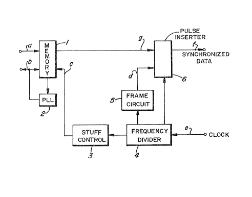
be described with re~erence to Fig. 2. In Fig. 2, re~erence
numerals 1 and 11 are buffer memories, 2 and 12 are phase
lock loop ~PLLi circuits, 3 is a stuff control circuit, 4 and 14
are frequency dividers, 5 is a frame signal generator~ 6 is a
pulse inserter, 13 is a destuff control circuit, 15 is a
synchronization circuit and 16 is a clock extraction circui~O
In Fig. 2~a), the data ~ is written into the bu`ffer
memory l in synchronization with a write clock signal ~ havin~
a bit rate of 704kb/s output by the PLL 2. This clock signal
is generated as indicated below from a high frequency clock
signal ~ . Namely, the clock signal ~ is divided by the
divider 4 to provide the basic frequency required for forming
the frame and is then subjected to stuff control (extraction of
a clock signal~ in the stu~f control circuit 3 so that a constant
stuff rate can be obtained ~3/8 in the example of Fig. l). Namel ,
as a result of stuffing ~insertion of dummy pulses), the
~6~
outp~t pulse train ~ or the stuff control circuit 3 has a
pulse frequency of 704 kb/s with a timing such that a dummy
pulse can be inserted as the leadlng bit position of ~he G3
frame when the main frame synchronization pulse SF is "1"
and the read operation o~ data from the buffer memory 1
is inhibitted. Moreover, the phase o~ the output pulse
train ~ is synchronized by the PLL clrcuit 2 and such
pulse is output as the clock signal ~ . Simultaneously, an
output of the frequency divider 4 is used to drive a frame
signal generator 5 which generates the required frame signal
and forms a frame as shown in Fig. 1 at the output of
the pulse inserter 6.
A phase comparator in the PLL 2 compares the phase of
an output of a voltage controlled oscillator and the phase
of the read clock signal ~ , and therefore it is enough for ~he
buf~er memory 1 to have the capacity to absorb only the fluctua-
tion o~ phase due to the ~rame ~it, stuf~ bit and stuf~ designatio
pulse insertion.
With the aforemen~ioned structure, the data signal written
in the buffer memory 1 is read by the clock signal ~ ,and
is then sent to the pulse inserter 6 as the data ~ . In
the pulse inserter 6, the frame signal O is inserted into
the data O as described above, and the frame as shown in FigsO
l(a) and l(h) is formed and is output to the transmission line
as the synchronized output data ~ .
The time at which the main ~rame synchronization pulse
SF becomes "1" matches the time at which the read operation of
~'~ -6~
~ .'
~ I 9,9' '- 1 1
buffer memory 1 is inhibitted. When the read operation is
inhibittQd, the data ~ to be input to ~he pulse inserter
6 is logic "0" and it becomes the dummy pulse.
The synchronized output data ~ sent to the transmissi.on
¦ line is re.-eived by the clock extraction circuit 16 in
the receiver shown in Fig. 2~b) and the synchronized clock
0 is extracted. The subframe synchronization pulse F and
the main frame synchroniza~ion signal SF are removed from
the synchronized data ~ in the synchronizer 15 and only the
data 0 in signal Q is written into the ~uffer memory ~l.
; Meanwhile, the synchronized clock input ~ is divided ~y
; the divider 14 and a timing signal for extraction of sub- and
main-fr me synchronization signals is output to the synchronizer
15~ while a timing signal ~or writing data to the buffer memory
ll is output simultaneously to the destu~f controller 13. In
the present invention, the data which indicates existence or
nonexistence of a stuff pulse in the transmitter is contained
in the code train of the main fxame synchronization siynal SF
and it is also used as the stu~f designation pulse.
l In the destuff controller 13, the data corresponding ~o
i the stuff designation pulse can be obtained from the code train
of the multiframe synchronization signal SF. Namely, the data for
judging existence or nonexistence of the stuff or dummy pulse
V can be obtained. The multiframe synchronization signal SF
l indicates that the stuff pulse V does not exist when it is "l"o
¦¦Therefore, when S~ = "0", the leading pulse in the G3 frame
7-
126Z~
is ~dged as part of ~he data. On the other hand, the synchron-
ization signal SF indicates that the stuff pulse exists when
¦it is "1". In this case, the leading pulse in the G3 frame
is judged as invalid, i.e., it is not included in the data
I ~ . In accordance with the value or the SF bit, the destuff
¦controller 13 inputs the clock signal ~ to the buffer memory so
~that a valid data pulse is written to the buffer memory 11
but the writing o~ the invalid ~stufr or dummy~ pulse V
is inhibitted. Such clock pulses are extracted and the phases
of them are averaged by the PLL circuit 12 and a clock
signal ~ corresponding to the original low frequency
clock signal ~ can be xecovered at the output of the PLL
circuit 12. The data in the buffer memory 11 is read by the
recovered clock signal ~ and thereby the data output signal
can be obtained at a re~uency of, e.g., 704 kb/s.
The stuff controller 3, freauency divider 4, frame signal
generator 5 and pulse inserter 6 are described in more detail
with reference to Fig. 3 and Fig. 4. In Fig. 3, 10 is a
~requency generator which generates clock signal ~ ; 31, 51~S4,
58, 59 and 61 are NAND gates; 41, 42 and 43 are ~req~ency
dividers; 32 is an AND gate with an inverting input' ~5 and 56
are inverters; and 62 is an AND gate. The signal wa~eforms of
respective portions in Pig. 3 are indicated by the same symbols
in Fig. 4. In Fig. 4, F is the code train of the subframe
synchronization signal, while SF is the code train of the multi-
frame synchronization signal and FF is the frame formatO
~ 3~7
-The opera-tions of the embodiment illust~ated in Figs. 3
and 4 is described below. The clock signal ~ generated by
the generator 10 is input to a divider 4, divided by 85 in the
divider 41 and output as clock signal CLl, because one G frame
is composed of 85 bits. The clock signal CLl indicates the
frame signal position of each G frame. The clock signal C~l
is further divided by 3 in the divider 42 and is then output
as clock signals CL2, CL3 and CL4 at different times, i.e.,
with different phases.
The output of clock signal CL2 indlcates the occurrence
of the G3 frame, while clock signal CL3 indicates the occ'urrence
of the G1 frame and clock signal CL4 indicates the G2 frame.
The clock signal CL3 is input to the divider 43 which outputs
a~clock signal CL5, which is CL3 divided ~y 2, clock signaI
CL6, which is CL3 divide~ by 4; and clock signal CL7, which
is CL3 di~ided ~y 8. -
-The clock signals CL5 and CL7 are inverted ~y in~erters
55 and 56. The outputs CL5 and CL7 of the inverters 55 and
56 are supplied to the NAND gate 58 along with the clock signal
CL6, while the clock signals CL5 and CL7 are supplied directly
to NAND aate 54. The outputs CL8 and CL9 of the NAND gates
54 and 58 are supplied to NAND gate 59 which outputs a clock
signal CLlQ.
The clock signals CLl, CL2 and CL5 are input to the NAND
gate 51 and the subframe synchronization signal F is output
therefrom. In addition, the cloc~ si~nals CLl, CL3 and CL10
are input to the NAND sate 52, and the main frame synchronization
signal ~namely, the stuff designation pulse) SF is output there-
from. The clock signals CLl, CL4 and CL10 are input to the
NAND gate 31 and the stuff control pulse SFP, which conducts
~62~3~
extractiorl of clock si.gnal ~ three times for each multiframe,
is output therefrom.
An output of NAND gate 31 is input to the inverting input
terminal of AND gate 32. The clock signal ~ is input to
the other input of the AND gate 32, and the clock signal ~
which is extracted by the stuff control pulse SFP as descri~ed
above, is output from the stuff control circuit 3. On the
other hand, the subrrame synchronization signal F and main
frame synchronization signal SF are input to the NAND gate 53,
the output of which i5 input to the NAND gate 61 and AND gate
~ 62 of the pulse inser~er 6 as the synchronization signal
_ The input signal ~ read from the buffer memory 1 is
input to the other input of NAND gate 61 which inhibits the
output of the synchronized data ~ignal ~ in accordance wlth ~he
pattern of the synchro~ization signal ~ generated by the
subframe synchronization sisnal F and the main frame synchroni-
zation signal SF. When the output of the NAND gate 53 has
logic level "1", the synchronization signal ~ , which is a
combination of the sub~rame synchronization signal F and the
main ~rame synchronization sign~l SF, is output :Erom the AND
gate 62.
Next, practical examples o~ the divider 14 and destuff
control circuit 1~ in the receiver are described with reference
to Fig. 5. In Fig. 5, reference numerals 141, 142 ~nd 143 are
dividers, and 131 is a NAND gate. The clock signal ~ extrac~ed
hy the cloc~ extraction circuit 16 and the synchronized data
received over the transmission line are input to the synchroni-
zation circuit 15. In the circuit illustrated in Fig. 5, the
~,,
~2~
nframe synchronizaticn signal F and main frame synchronization
~cignal SF are removed from the synchronized data ~ , ~ut an
,loutput of divider 14 is fed back to the synchronization circuit
15 in order to loc~ the phases of the output of divider 14
and the synchronized data ~ .
~~ In the divider 14, the frequency dividing circuits 141 and
142 formed in the divider 14 respectively have the same functions
as the frequency dividing circuits 41 and 42 in Fig. 3. Divider/
logic circult 143 corresponds to dividing circuit 43 plus
gates 54-59. As described regarding Fig. 3, an output of ~he
dividing circuit 141, corresponding to the clock signal CLl
in Fig. 3, an output of the divided circuit 142, correspondlng
to the clock signal CL4 in Fig. 3, and an output of the dividing
logic circuit 143, corresponding to the clock signal CL10 in
Fig. 3, are input to the NAND gate 131 which forms the destuff
control circuit 13, in order to provide -the destu~f timing.
Thereby, the pulse indicated as SFP in Fig. 4 is input to the
buffer memory 11 from the NAND gate 131. The buffer memory 11 is
inhibited from writing the synchronized data Q when the pulse
SFP is generated.
As descri~ed abo~e, according to the present invention,
the multlframe synchronization signal is also used as the stuff
designation pulse SF. Therefore, the stuff desi~nation pulse
SF can be transmitted even when the conversion ratio (difference)
between internal memory rates and transmit rates is small.