Note: Descriptions are shown in the official language in which they were submitted.
- 1 - 6~59-921
RADIATION HARD GATED FEEDBACK MEMORY CELL
BACKGROUND OF THE INVENTION
1. FIELD OF THE INVENTION
This invention relates to bistable regenerative solid
state memory cells, and particularly to such cells where redundant
elements are employed to protect the logic state of the cell
against upset due to radia-tion.
2. ~ELATED ART
Prior art reveals a basic known solid state bistable
regenerative memory cell. Random access memories (RAMs) use a
matrix of such cells, each adapted to be uniquely written into or
read.
Radiation, such as alpha particles or cosmic rays, cause
transients in memory cells as they penetrate into the cell. These
transients can trigger the bistable circuit by changing the
current or voltage at a transistor node thereby causing the cell
to switch logic states.
In bipolar memory cells, the causes oE such radiation-
induced upset are primarily (1) collector nodes of OFF transistors
~an short to ground, and (2) base nodes of OFF transistors can
short to collector nodes turning OFF transistors ON. The first
mechanism is the dominant cause of single event upset (SEU) in
.~
,9~
--2--
cosmic ray environments. This mechanism, with small
variations in charge collection volume and circuit upset
thre~hold, is also found in other semiconductor
technologies such as NM3S/Si and CMOS/Si~
The second upset mechanism is found only in
bipolar devices. Here a parasitic current path is
formed within the device i~self rather than between the
device and the substrate~ The second upse~ mechanism
involves a smaller amount of upset charge which can
still cause upset at high LET values (LET denote~ linear
energy transfer, which is the amount of energy deposited
in the semiconductor by the radiation). It i5 e~timated
that if the first up~et mechanism is eliminated
completely, then ~he second upset mechanism will still
limit the error rate to about lE-7 (i.e., lxl0-~) errors
per bit-day.
~arious techniques have been propo~ed for
hardening pipolar circuits to SEU. However, all of
the~e techniques address only ~he first type of up~et
mechanism listed above. They propose to ei~her remove
the collector ~rom electrical contact wi~h the substra~e
or reduce the charge injected into the collector node.
The most effective of these other technique~
dielectric isolation - completely isolates the collector
from the substrate.
--3--
Eliminating SEU-induced collector-to-base
shorts is much more difficult. Pulse rise time can be
used to discriminate S~U currents from normal device
currents. This forms the basis for CMOS hardening by
means of cross-coupled resistors or extra capacitance.
But this ~echnique degrades the speed of bipolar
circuits so much that they lose their competitive
advantage against CMOS.
Phctocurrent compen~a~ion techniques are also
ineffective against the second form of SEU because the
upset current varies with ~he direction o ion
incidence. Geometric effects practically rule out the
location of a secon~ charge collec~ion region which can
produce an equal but oppositely directed photvcurrent
from the same ion path. Finally, circumvention
techniques are almost totally ineffective beca~se of the
difficulty of sensing a time-random ion event at every
transistor node and recovering fas~ enough (~Og.~ 0.2ns)
to prQvent an upset.
A bit error rate of lE-10 error/bit-day is
being sought for memory elements in a cosmic ray
environment. This corresponds to approximately ~hree
year~ without an error for a one megaword memory. Only
one technology (CMOS/SOS) can meet this goal at present,
bu~ CMOS/bulk Si is constantly being improved and may be
able to meet this goal in the near future. No bipolar
technology, however J can approach this goal,
~2~2~
- ~ - 6~159-921
Ever mo-re stringent error/bit-day rates are highly
desirable with the enormous increase in memory capacity being
projected for general purpose computers. In a general purpose
computer an error in the register bit or memory bit can be
retained and used in a number of calculations. ~f the bit is a
critical value, the consequences of even one error can be
disastrous.
It is th~s highly desirable to have a memory cell which
is extremely resistant to both types of SEU. It is further highly
desirable to have such a cell which is adaptable to either
unipolar or bipolar transistor circuits.
In accordance with this invention there is provided a
solid-state gated feedback memory cell which will retain its
current logic state despite the introduction of certain transient
electrical signals at certain locations within said memory cell,
comprising:
first, second, third and fourth switching means, each of said
switching means having a Eirst region, a second region and a
~ontrol region, wherein said ~irst and second regions are doped so
as to be partially conduGtive and wherein said control region
controls the flow of current between said first and second
regions, wherein said first regions of said first and second
switching means are connected at a first node and said first
regions of said third and fourth switching means are connected at
a second node,
first, second, third and fourth load means, wherein said
first load means is connected to and between said second region of
said first switching means and a third node, said second load
.... - ., .
1,'~6~
- ~a - 6~159-921
means is connected to and between said second region of said
second switching means and said third node, sai.d third load means
is connec-ted to and between said second region of said third
switching means and a fourth node and said fourth load means is
connec-ted to and between said second reglon of said fourth
switching means and said fourth node;
Eirst, second, third and fourth isolation means for
controlling electrical signals applied to said control regions,
wherein said first isolation means is connected to and between
said first load means and said control region of said third
switching means~ said second isolation means is connected to and
between said second load means and said control region of said
fourth switching means, said third isolation means is connected to
and between said third load means and said control region of said
second switching means and said fourth isolation means is
connected to and between said fourth load means and said con-trol
region of said fourth switching means; and
wherein said first and second nodes are connected to a first
voltage reEerence point and said third and fourth nodes are
connected to a second voltage reference point, so that dlfferent
voltages may be applied to said first and second voltage reference
points to supply electrical energy to said cell, and wherein said
load means~ said isolation means and said switching means for~l a
bistable regenerative device with logic values provided at said
second regions, and wherein if said transient electrical signals
are introduced at only one of said second regions, the logic
values of the remainder of said second regions ~Jill be unaffected,
- 4b - 64159-921
SUMMARY OF THE INVEN~ION
The present invention is a bistable solid state
regenerative memory cell wherein redundant switching means, such
as bipolar or unipolar transistors, are connected in a cross-
coupled arrangemen-t. Each transistor has a load connected between
the transistor and a voltage referenced current source. Means to
control the current or voltage applied to the base or control gate
of each transistor is provided between such base or control gate
and the collector (or drain) of the other transistor to which it
is crossed coupled.
Diodes are the preferred control means. Read and wri-te
circuitry is readily provided to allow the cell to be incorporated
in a RAM or a logic array~
.
:~f~
The redundant transistors and diodes serve to
retain the logic state of the cell de~pite an SEU
occurring at the collector ~or drain) of one of the
transistors.
~IEF P~RIPTION QE T~E ~RA~IN~
Figure 1 is a prior art solid state
regenerative bistable cell.
Figure 2 is a generalized schematic of ~he
pre~ent invention.
Figure 3 is a DTL version of the present
invention.
Figure 4 is the cell. o Figure 3 with read and
write circuitry added.
Figure 5 is an SDFL version of the present
invention.
DE~RIP~I~N OF THE ~R~FERR~D EM~Q~IM~NTS
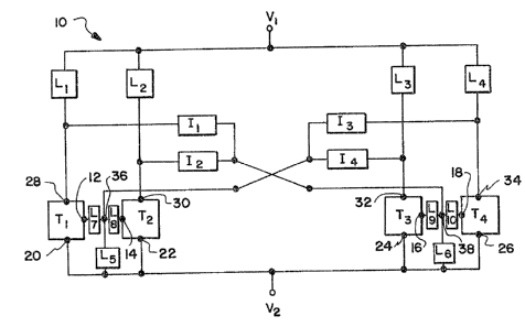
Figure 2 shows the present invention, i.e., a
solid state memory cell 10.
Two cross coupled pair~ of switching means,
such as transistors, are shown as Tl/T2 and T3/T,~. Each
transistor includes a control region ti.e., 12, 14, 16
and 18) which is either the gate of a Eield effect
transistor or the base of a bipolar ~ransi~tor. The
con~rol region in each transistor controls the voltage
or flow of current between a f irst region (i.e., 20, 22,
24 and 2~) and a second region (i.e., ~B) 30, 32 and 34)
of each . ransistor.
~26'~
--6--
Load means Ll, L2, L3 and L~ are connected
between a first voltage reference point V1 and second
regions 28, 30, 32 and 34, respe~tively.
Isolation means Il, I2, I3 and I4 for
5 controlling the voltage or current applied to the
control regions are connected, respectively, between
second region 28 and control region 16, second region 30
and control region 18, second region 34 and control
region 12 and s~cond region 32 and control region 14.
Load means Ls may be provided between common
base node 36 and a second voltage reference point V2J
Similarly, load means L6 may be provided between common
base node 38 and second voltage reference point V~.
Load means Ls and L6 are important to the WRITE process
when the transistors are bipolar. Writing into the cell
will be discussed further below.
Load means L7, Lg, Lg and Llo are each
connected between the control regions of one of the
transistor~ and their respective cross coupling
20 isolation mean~, Thes~ further harden the circuit
against radiation and will be discussed further below.
Note that nodes 36 and 38 are convenient points
for connec~ing a WRIT~ means.
Operation of cell 10 (Figure 2) is as follows.
25 Assume tha'c Tl and T2 are O~, and T3 and r4 ar~ OFF.
The vol~ages at the second regions 28 and 30 are
--7--
low (e.g., a logic 0) since Tl and T2 are in their low
impedance state. The current through Il and I2 i5
insufficient, therefore, to raise the potentials of
control regions 16 and 18 enough to switch ON either T3
or T4. Thus T3 and T4 remain OFF. In turn, the second
regions 32 and 34 are high (e.g., logic 1). I3 and I~
are devices which will provide sufficient voltage or
current to control regions 12 and 14, respectively, to
keep Tl and T2 ON when second region~ 32 and 34
respectively are in a high state. Since I3 and I~ are
connected in common at node 36~ if ei~her I3 or I4 are
providing sufficient voltage, or current, then both T
and T2 will be ON. Similarly, due to their common
connPction at node 38, either Il or I2 will provide
v~lt~,~
~ufficient -~t~ ~ or current to keep T3 and T4 ON if
either node 28 or node 30, respectively, is in a high
sta~e.
If the transistors in Pigure ~ are bipolar, the
electrical signals controlling them will be currents
~ransmitted throuyh the isolation means Il through I~ to
their respective base regions. If transistors in Figure
2 are FET~; the electrical signals transmitted by the
isolation means Il throuhg I4 will be voltages applied
to their respective gate regions.
8 6~159-921
Consider the invention if the memory cell is hit by a
single event pulse. For example, in DTL circuit 40 oE Figure 3,
assume that initially T3 and T4 are OFF, and that T3 is hit by a
heavy ion which -funnels charge into its collector node 32. Then
collector node 32 is pulled to ground. Diode I4 gets reverse-
biased, isolating node 32 from the rest of the circuit~ Diode I3,
however, stays forward-biased maintaining the base current oE Tl
and T2. Thus Tl and T2 stay ON, the collector nodes 28 and 30 oE
Tl and T2, respectively, stay low and diodes Il and I2 remain
reverse-biased. Transistor T4 stays OFF, ensuring that the state
of the cell is not changed.
As soon as the transient charge on collector node 32 of
T3 is dissipatedfe.g., 0.5 ns) the potential at collector 32 rises
to the same level as collector 34 of T4. Cell 40 has thus
survived an SEU event with its information intact with only -the
appearance of a transient state which may or may not be observed
on later readout.
Readout from the cell can be accomplished by numerous
convenient meansO For example, for cell 40 one could use (a)
Schottky diodes coupled to collector nodes, (b) multiple emitters
on transistors or (c) Schottky diodes coupled to base nodes.
Figure 4 shows scheme (a) with transistors T5 and T6 coupled to
regions 28 and 344, respectively.
t~
6~
g
It is not necessary to sample both current
paths on each side of the flip-flop for readout. If a
single event pulse affects one current path while
readout is being accomplished on the other path, the
S event will go unnoticed and the correct logic state will
result. If a single event pulse affects the same
current path that is used for readout, the effect is the
same as if a single event pulse hit one of the
transistors in the logic chain between the cell an~ a
following register or output pin. Therefore, there i5
little reason to harden one part of the chain unless the
other (larger) part of the chain is hardened also.
Voting on three successive readouts of the cell will
eliminate all errors incurred during cell readout, both
inside and outside the cell.
Writing the cell requires forcing a current
into the base node of the OFF transistors which is
larger than the base current provided inside the cell to
the ON tran~is~ors. This is accomplished, conveniently,
20 with transistors T7 and T~ coupled, respectively, to
nodes 42 and 44 as shown in Figure ~. The time for 'che
cell o switch f rom one s'cate to another i~ related to
the time required to pull charge out of the base regions
of the initially ON transistor~ (e.g. T3 and T4). WhPn
2s the initially OF~ transistors are switched O~ by the
externally supplied base current pulse, the diodes
--10~
on the collectors of these tran~istors become~
reversed-biased. This means that there is no way for
the base charge of the initially ON transistors to be
withdrawn unless one supplie~ a leaka~e path ground.
This is accomplished (in Figure 4) by base pull down
load mean8 Ls~ L6~ L7 and L~.
The cell must be accessed from both side~ in
order to WRITE both states successfully~ This means
that somewhere in the WRITE circuit there is a
possibility of single-point failure. This failure can
result in an incorrect s~ate being wri~ten into ~he
cell. ~n ~igure 4, the single point of failure occurs
on the means whereby current is diverted from the base
of ~ransistOrs T7 ~nd T8-
Consideration of errors which occur in the
WRITE mode leads one to the conclusion that i~ is not
effective to harden iust the f2w transistors adjacent to
the ~orage cell unless all transistors in the logic
chain leading lnto the cell are hardened to near the
~ame level. This follows because all the ~rans~stors inthe logic chain have the same duration of susceptibllity
(the path delay time) and all are likely to have tbe
same critical charge and critical time. Therefore, the
probability of upset is approxima~ely the same~ This
mean~ that hardening the la~ N of ~ ~usceptible
transistors in the logic chain will result in a
reduction of the critical volume, and enhance the SEU
error rate, by a factor N/M.
In order to harden the cell again~t SE~ induced
collector-base shorts, load mea~9 Lg~ Llo~ Lll and L12
are preferably employed. Even though th~ teansistors Tl
through T4 are placed in separate isolation region~, the
transistors on one side of the cell share a common base
node. Therefore, collector-base current from one
transistor can affect the base current of the other
transistor on the same side of the cell, turning both
OFF tran~istors 0~ at the same time. This can be
alleviated by adding base resistors such as load means
Lg through L12 as shown in Figures 2 and 4.
Ion-produced single event upset currents from one
transis~or must go through both resistors (e.g. Lg and
Llo) before affecting the second transistor on the same
~ide of the cell. This ls a modified version of cross
coupled re~lstors, which in the pa3t has not been very
effective for bipolar SEU hardening. 8ut in the pre~ent
cell the collec~or~substrate component of upset current
cannot produce upse~, and the collector-base component
i~ much smaller than the normal collector-substrate
component. Therefore, the re~istor values c~n be
relatively small and the circuit is not ~lowed very
much.
--12--
A ~inal improvement which i~ highly desirable
to harden the cell against SEU is to provide isolation
mean~ and load means which are .inherently not
susceptible to SEU. If they are susceptible, SEU could
inject current into the base of both OFF transistors on
one side of the cPll, turning them both ON. Load means
Ls through L12 and isolation meanq Il through I4 are the
most important means ~o be hardened against SEU.
Hardening of these elements o~ the cell can be
lO accomplished by providing thin film poly~ilicon
resistors as the load means and using an implanted
dielectric under Schottky diodes as the isolation mean~.
By itself, the gated feedback cell is of course
only part of an integrated circuit. For a complete
circuit, this cell can be embedded in ei~her a RAM, an
edge-triggered flip-flop, or a register file (which is
an array of edge-trigyered flip-flops.) The area
penalty for R~M design is approximately 100%. The area
penal'cy or an edge-triggered flip-flop can be as low as
~5~ if only the output latch is protected. ~his may be
possible in the edge-triggered fllp-flop scheme becau~e
the remainder of the edge-~riggered flip-flop is used
only during the input operation. This make~ the cell of
the presen~ invention an a~tractive solution for
register files and stand alone flip-flop~.
-13-
Implanted resistors with implan~.ed dielectric
isolation can also be used instead of polysilicon
resis ors to harden the load means. In addition to
implanting a dielectric under a Schottky or junction
diode to harden diodes, some other techniques available
for hardening diodes are (a~ implanted polysilicon
junction diodes t (b) Schottky diodes in recrystallized
~ilicon over insulating sub~trate material, and (c)
Schottky diodes in double epitaxial material, where the
second epitaxial layer i5 grown in a V-shaped region
surrounded by oxide with the original epitaxial layPr as
the floor. Presently, implanted dielectric under the
Schottky diode is the preferred option.
Edge-triggered flip-flops are only one of three
types of sy~chronous clocking schemes commonly used by
logic designers. The other two are master-slave latches
and multi-pha e clocking with logic between the
latches. Each of these clocking cheme~ can be
implemented in various circuit families. The gated
~eedback cell can be used with any of these clocking
schemes.
/~ V'CI /V C,`S
The choice of clockin~ scheme ~ e~ a
tradeoff o~ system speed, clock skew problems, minimum
pa~h delays problems and ease of architectural d~sign.
The choice will be highly application dependent.
-14
Figure 5 shows a version of the present
invention applied to GaAs SDFL technology. READ and
WRITE means are not shown~ ~owever various ~EAD and
WRIT~ means well known to those skilled in the art can
be employed. Yigure 5 employs metal-semiconductor F~Ts
in the depletion mode; however, enhancemen~ mode FETs
Jdc~/~f ,`o ~
can be employed as well as ~e~ ~t~on-doped FET's
~MODFET's).
When MESFETs are employed, GaAs is the
preferred substrate material; however, silicon or other
semiconductor materials can be used for the substrate
with the present inventionO