Note: Descriptions are shown in the official language in which they were submitted.
~3~
.` 1
The present invention relates to an arrangement for establishing a wide band
connection in a switching network in telecommunication equipment operating
with pulse code modulation and time division multiplexing, where the connec-
tion comprises two or more channels.
5 The invention is intended for use in telscommunication systems which divide
the bit flow up into a plurality of channels for a predetermined number of bits,e.g. 64 kbit channels, which applies to such as the AXE type of system.
In such systems is a need of being able to establish high quality connections,
e.g. connectiorls for video transrnission. This means, inter alia that a sampling
10 rate must be enabled which is higher than that applicable to the basic system.
The problem is solved by two or more channels being combined and thus
creating a so-called wide band connection. Such channels which form a wide
band connection must be monitored on establishing communication in the
switching network so that the respective contents/samples are not mutually
15 delayed, since there is distortion in the transmitted information if this delay
takes place.
For solving this problem it would be possible to modify the group selector
(switching networ)k in the respective station/exchange, where its modification
would mean that the selection of internaI time slots must be cantrolled for the
20 wide band connection.
The time slots must then be selected so that writing intn/reading from the
speech memories of the channels included in the connections i9 carried out with
the information kept together. Such a modification can be performed entlrely in
thc software.
,
''
~'. ''' . ..
. . ' ~ '
'~ , ,
~ ~ 3 ~
The solution proposed above also involves large disad-
vantages, however, since the internal time slots cannot be at a
free disposal, which causes the probability of congestion to
increase. The probability of congestion also appears to be
dependent on the mutual relationship of incoming and outgoing
time slots. The increased probability of congestion will thus
extend the mean connection time.
An alternative way of solving the problem mentioned is
that when local or transit nodes are through-connected, a poss-
ible mutual delay is allowed to take place, due to the transfer
between external and internal time slots, and to equalize the
possible delay between the contents of the channels after the
through-connection has been completed in the swi-tching network.
According to the invention addresses during a connec- :.
tion establishment stage the switching network input is supplied
with specific information as to the respective phase position of
the channel contents, and that at the output of the network this .
specific information is detected and delays are regulated in
means for equalizing the contents of the channels.
~ ccordingly, there~ore, the present lnvention provides
an arrangement for establishing a wide band connection in a
switching network in telecommunication equipment operating with
pulse code modulation and time division multi-plexing, where the
connsction comprises two or more channels, comprislng marking
means disposed at the switching network input such that, durin~
the establishment of a connection, the marking means lnsert mark-
ings in a plurality of successive frames o~ the respective con-
tents in the time slots utilized by the connection rh2nnels~ the
marking means assigns to each affected time slot in a first frame
a first marking, the effected time slot in a second frame a sec- .,
ond marking, and so on~. until the number of such successive
frames is e~ual to a maximum time displacement in the switching
network, this displacement corresponding to a number of frames
'
- 2 - `
' ~ .
,; ~
, .
. , .
,
~2~i3~6~
plus a constant and scanning means disposed at the output o~ the
switching network, which detects a pattern formed by said mark-
ings and by means of said pattern conflrms a possible delay
between the respective contents of the channels, due to the con-
nection process in the switching network, and sald scanning meanscontrolling means for equalizing delays in the channels so as to
ensure that, after the establishment of the connection, the con-
tents of the channels/time slots regain their mutually synchro-
nized positions, in spite of the possible, mutual delay.
- ~
What may be more concretely considered as characteriz-
ing for the new arrangement is, inter alia, that a marking means
is disposed at the switching network input such that during a
connection establishment stage the means applies markings in a
plurality o~ successive frames of the respective contents in the
time slots utilized by the connection channels, and that a scan-
ning means is disposed at the output of the switching network
such that the scanning means detects a pattern formed by said
rnarkings, and with the aid of it determines a possible delay
between the respective contents o~ the channels, due to the
through-connection process in the switching network. A further
characterizing feature is that scanning means c~ntrols delays
equalizing means in the channels so that the equalizing means
~ ensures that, after the connection establishment stage, the con-
2s tents of the channels/time slots regain their mutually synchro-
nized positions in spite of the possible, mutual delay.
- 2a -
. . ' .
~63~g
f ~ , I n \/ l~ r~
In ~}P~e~eF~lbe~ t, the content in each aFfected time slot in a first
Fl~llle iS assi9ned ~3 first rnarking, tlle content in eacll affected time slot in a
second frame a second marking, and so on. The number of frames marked thus
is selected such that it is equal to a number of lFrames corresponding to a
5 maximum diFference in the time displacement in the switching network,
reckoned as a number of frames plus the constant two. A group with the
rnentioned number of frames is followed by a corresponding group of frames
where the nnarking of the contents in the different time slots is carried out in a
corresponding manner.
10 The aforementioned means preferably includes a means carrying out the
markings in the respective frame and adapted such that in response to the
comparison it feeds instructions to a memory included in said equalising means.
The equalisiny means may include two or more parallel paths for the bit flow
departing from the switching network. The first of said paths lacks delay, the
15 second delays the bit Flow a frame length, the third delays the bit flow two
frame lengths, and so on. The equalising means guides the contents in the
channels into different paths in response to the instructions obtained from the
comparison means.
With the aid of the inventive arrangement wide band connections can be
20 established without the respective group selector/swltching network needing to
be modified for the connection in question. The equipment required for
rnarking, detection of the marking and establishment of the connection can be
assigned to the wide band connection as such, which may be advantageous for
determining the cost carriers within the system.
25 The invention will now be described in more detail, by way of examplè
on:Ly, with reference -to the accompanying drawings, in which:-
Flgure l illustrates the principle of marking the conten-t in channels/
time slots in a plural:~-ty oE successive Erames;
I ic3ure 2 is a table (a pattern) of the marking oE Erames and channels on
30 Ihe input side of a switching network/group selector;
,.
~ ,
.' ~ . ::
~63~
i(JI11`~3 21 i~; a tal~le (a pattern) or the rnarkinys of tl-e frarnes and channels on
tlle output side oF thr3 switchirly network/group selector
Figure 3 is a principle sketch illustrating the means carrying out the markings,(iisposed at the input of tlle switching network ~group selector), and
5 Fiyure 4 illustrates detection means for detecting the rnarkings and means
delays in the channels.
The invention is intended for use in through connection of wide band connec-
tions in group selectors or corresponding units associated with telecomrnuni-
cation equipment working with pulse code modulation and time division
10 multiplexing. The telecornmunication equipment can be of the AXE type, which
divides the bit flow into 64 kbit channels with the sampling frequency of 80D0
samplings/s wikh 8 bits in 256-bit frames.
Firgure l illustrates six such sequential frames 0-5 in series one after the other
in a connection not illustrated in the figure, to a group selector or correspon-
15 ding unit.
In accordance with the invention, the contents in the time slots which are usedas channels in the wide band connection are marked on the input side of the
group selector. In the ernbodiment it has been assumed that three channels are
included in a wide band connection. The three time slots utilized in these three20 channels have been marked with a,b and c in a first group of frames A, and with
a', b' and c' in a second group B~
The respective three tirne slots in respective frames n-5 have been shown
placed adjacent each other, although the tirne slots can be spread within the
respective frame.
25 The time slots a in frarne O are rnarked identically the same and the markingconsists in the present case of the binary value O which is illustrated with thenumeral value O in Figure l, for the sake of simplicity. The 910ts b in the frame
l are marked in a corresponding manner with the binary value 1 and the time
slot-s c in the frame 2 with the binary value 2.
" .
~" ` , ,:
: ~... . .
~63~ii9
Ihc tiloe slo~r. a' in the fralrle 3 are marked as i9 the time slot a in frame O.
~ (` tilOC 910t l)MIl rrarl)e 4 iS marl<ed as is the tilne slot b in frarrle 1 and the
lilne slot c' in frame 5 as is the tirne slot c in frame 2.
Tl-e numoer o F individual rnarkings, i.e. the number of frames within the
5 respective group A, B is dependent on the maximum difference in time
displacemerlt which can occur in the group ~elector (switching network)
reckoned as a number of frames. The number of individual markings is thus
equal to the maximum displacement plus a constant 2. Since the contents in the
ti1ree channels in the AXE-type system may be mutually delayed by at most one
10 frarne there is obtained a plurality of individual markings, which will be three in
the present case.
The number of groups A, B is dependent on how long a time it takes to
deterrnine the mutual difference. The groups of frames consecutive to the
group B in Figure l have corresponding structure and marking as the yroups A
15 and B.
Figure 2 illustrates in the form oF a table the marking/pattern according to
Figure l, i.e. how the marking appears on the input side of the group selector.
In the table the frames have denotations corresponding to the frames in Figure
l. The channels utilizing the time slots in a, b, c etc have been given the
20 denotations O', l', 2' in the table.
Figure 2a illustrates how the content in the channel l' is delayed in relation to
the contents in the channels 0! and 2'. The delay here is dependent on the
junction between external and internal time slots in conjunction with the
through connection in the group selector. This rneans that the contents in the
25 channels O' ancl 2' rnust be delayed a frame length before the bit flow i5 sent
further to the outgoing line.
According to Figure 3, the bit flow comes from the line L. Marking of the
content in the respective channel/time slot takes place with the aid of a
pattern generator M and a selector Vl which is controllable with the aid of a
30 control unit S. The selector Vl connects the line L to the group selector G via
L', and in response to orders from the control unit it can temporarily connect
.
~L~63~
tlle l~alt~3rn cl(-n~rator for marking the content in the respective affected time
3 ~ S.
The control unit includes a rnemory rm, irlto which the prerequisites for the
operational mode of the control unit are written frorn an unillustrated superior5 unit. Writing t~kes place via a conductor l1 and addressing to the different cells
(0-31) with the aid of the selector means V2 controlled via 12. Thcre are two
control orders: order I "Collect from the line" and order 2 "Collect pattern".
The control order stored in the mernory m are read with the aid of a channel
counter K, counting between 0-31 and contrDlled by a 256 kHz signal via 13 and
10 a synchronizing signal of 8 kHz via the line 14. Actual reading from the memory
m is done by the selector means V3.
The pattern generator M includes registers R1, R2 and R3, the outputs of which
are connected to an OR gate OR, the output of which is connected to position 2
in the selector means V1. lhe respective register generates the markings û, 1
15 and 2~ in binary form.
The respective register has two control inputs stl ànd st2. The first input is
controlled by a counter CNT which, in response to control from the frame
synchronization of 8 kHz via st3 activates the respective register. The control
input st2 obtains a clock pulse of 256 kHz from a clock pulse source in the
20 telecommunication equipment and control input ST2' obtains a clock pulse of
2048 kHz from tlle same source.
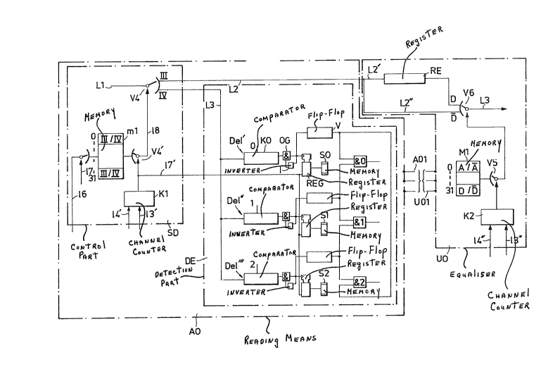
In Figure 4 there is illustrated a reading means AO, which detects a pattern
forrned by said markings, and with the aid of the pattern determines the
possible delay between the contents` of the channels.
Z5 The means AO includes a control part SD a detection part DE, a selector meansV4 and a memory ml, in which are written the orders from a superior unit,
these orders applying to the selector means V4. The latter has two order
positions: position 3 which is a normal position, and position 4 which is a
position for analyzing delayed time slots (channels).
-
.
.
~263~
Writi~ into tbe memory rnl takes place Vi1 a line 16 and addresslng to the cells0-3l via a lh-e 17. Time slot control is obtained from saicl superior Ullit. Reading
out From tl)e memory ml is controlled Frorn the channel counter Kl via the
lines 13', 1~' in a corresponding way as the memory m is controlled from the
5 chanllel counter K. Read out from the memory ml for control of the selector
means V4 takes place via a selector means V4', and a line IE;-
The detection part comprises a plurality of identically implemented parts Part',Part", Part"' the numbPr of which corresponds to the number of patterns used.
The respective part includes a comparator KO, The output of the respective
10 comparator Is connected to an AND gate OG, the other input oF which is
connected to an inverting means I loopconnected from the AND gate output.
There is further included a register REG, the output of which is connected to
its respective memory SO, 51 or 52. The respective output on the AND gate OG
is connected to both the register REG and a flipflop V. An input on the
15 respective register REG is also connected to the output on the channel counter
Kl.
The respective one of said identically implemented parts is adapted for reactingto its individual marking. Accordingly, the Part' reacts for the marking O, the
Part" for the marking 1 and the Part"' for the marking 2.
2û Tl-e output from the respective flipflop V in the parts Part' and Part" is
cunnected to an AND gate &O, the output from the respective flipflop V in
Part" and Part"' to an AND gate &l and the output on the respective flipflop in
Part"' and Part' to an AND gate &2.
In accordance with the example in Figure 2a there is obtained a pattern 0, 2, O
25 from the scanned frame. The comparator KO in Part' reacts for the marking O
in the time slot zero, resulting in that the flipflop V in Part' is set, and that the
channel address for the time slot in question is written into (stored in) the
memory SO. The comparator in Part"' reacts for the marking 2 in time slot 1,
resulting in that the flipflop V is set in Part"', and that the channel address for
30 the time slot in question is written intu (stored in) the memory S2. What hasnow been sald slgniFies that the AND gate &Z sets its output to a One. The
'` .. '
63~
co~ roLc)r in P;~rt' reacts for the marl<ing ~ero in the time slot 2 and the
cb.Illnr31 acl(lre3s for this time slot is also written into (stored in) the memory
50.
A first order or instruction i5 thu~ delivered from the outputs of the AND gates~cO, &l and &2. Other One settings of the AND gate outputs result in different
outgoing instructions, etc.
Figure 4 also illustrates a means UO equalising delays in affected channels. Themeans UO includes a memory Ml, which receives the instructions from the
means AO. The instructions in the memory Ml are read out with the aid of
selector means V5 which is controlled by a channel counter K2, in turn
controlled in a corresponding manner as is the channel counter K via lines I3"
and 14".
The means UC) includes selector means V6 with order positions D and D. The
line coming from the group selector is denoted by Ll in the Figure. The selectormeans V4 normally directs the bit flow to the line L2, but in the cases where
marked channels are to be identified towards the line L3, it directs the bit flow
to said detection means AO.
The line L2 branches into line paths L2' and L2". A register RE comprising a 256bit register of a known kind is linked into the line part L2'. The selector means
V6 connects the line L3 to one of the paths L2' and L2" decided by the mean~
UO.
The instructions from the output AOl formed in the means AO are trans-Ferred
to the rnemory Ml (the input UOl) in a known manner, e.g. with the aid of
known control system. In accordance with the above there are written into the
memory Ml the instructions set forth below, in response to what was obtained
on the outputs AOl, (the outputs &0-&2 of the AND gates)~
If all the AND gate3 d~Ode2 are set to zero, the order D (i~e. no delay)) is
written into the memory M1 for all the affected channels, the addresses of
which are written intostored in SO~ Sl or 52. If the gate &0 is set to One, D iswritten into the memory Ml for all channels having addres3es registered in the
.... .
''
. . , ~..... . .. . . ..
'' ~ ': :' . ` '
'.. " '~
~63~.~9
melllc)ry Sl, alld D for all channels havirlg addresses registered in the memory5(). Ir thc gate ~cl is set to One, D is written into the mernory Ml for all
charlnels havirlg addresses written in the memury ~2, and D for all channels
havincJ addresses written into the memory Sl. Finally, when only the gate &2 is
5 set to One, the order D is written into the memory Ml for all channels having
addresses written into the memory SO and D for all channels having addresses
written into the memory 52.
It will be seen from the above that what is delayed i5 only the content of the
respective channel included in the wide band connection since the contents of
10 rernaining time slots in the respective frame are shunted via the order position
[~.
After generation of instructions to the memory Ml, the wide band connection is
made and subsequent frarnes will be guided in the line paths determined by the
memory Ml past and /or through the delay register RE, which delays the bit
15 flow controlled via the line path L2' by one frame length.
The equipment described hereinbefore is suitably included in terminal equip-
ment in connection with the group selector network. The terminal equiprnent is
duplicated in the case where two-way paths are to be established through the
switching network.
20 The invention is not lirnited to what has been described hereinbefore and
exemplified by the embodiment~ but may be subject to modifications within the
scope of the following claims and the inventive concept.
.
~' :
: . .
' . . ~
'' ~