Note: Descriptions are shown in the official language in which they were submitted.
~3~ 3
AUTOMATIC LEVEL CONTROI, CIRCUIT
FOR AN AD CONVERTER
Background of the Invention
The present invention relates to an automatic level
control circuit and, more particularly, to an automatic
level control circui-t applicable to a demodulator of a
multi-level quadrature amplitude modulation (QAM) system
and others.
The current trend in the art of microwave band
digital communications is toward the use of a multi-level
QAM system which enhances effective utilization of the
limited fre~uency band. In such a communication system,
an analog-to-digital (AD) converter at a receive terminal
compares a demodulated baseband signal with a plurality
of predetermined reference levels to thereby -transform
-the baseband signal to two-level parallel digital signals.
In this instance, the prerequisite is that the input level
o~ the baseband signal to the AD converter is maintained
constant relative to the reference levels despite possible
changes in the receive level and those in the gain of a
receive amplifier.
The above prerequisite has heretofore been met by
installing variable-gain amplifiers one before a QAM
detector and the other a~ter the QAM detector and
; : ~
'';
66446-367
controlling their gains by means of outputs of AD converters.
The problem with the prior art implementation is that,
as will also he discussed later in detail, the use of variable-
yain amplifiers which are adapted for stabilization of signal
level makes the circuit construction complicated and, thereby,
brings about the need for extra s~eps and time for the adjustment
of variable-gain amplifiers in the production line.
Summary of the Invention
It is therefore an objeet of the present invention to
provide an automatic level control circuit which is practicable
with a simple construction~
An automatic level control circuit of the present
invention for use in a multi-level signal transmission system
comprises an analog to-digital (A/D) converter for discriminating
a demodulated multi-level baseband signal with respect to a
plurality of reference levels to produce a plurality of decoded
digital signals and an exror digital signal, and a reference
voltage generator, including logic circuit means~ responsive to
said decoded digital signals and said error digital signal for
providing a reference voltage to said A~D converter to uniformly
shift sald plurality of reference levels, said reference levels
beiny controlled to optimum ones responsive to a variation in the
level o~ said input signal.
,. ~ . .
"' ' : .,.: :
. :. .: .
Brief Description oE the Drawings
The above and other ohjects, features and advantages
of the present invention will become more apparent from
the following detailed description taken with the
accompanying drawings in which:
Fig. 1 is a block diagram showing a prior art 16-level
Q~M demodulator, which includes an automatic level control
circuit.
Fig. 2 is a discrimination domain map associated
with a 4-level ~aseband signal;
Fig. 3 is a block diagram of an automatic level
control circuit for an AD converter embodying the present
invention;
Fig. 4 is a block diagram showing another embodiment
of the present invention; and
Fi~s. 5 and 6 are block diagrams representative
of two different applications of the automatic level
control circuit bf the present invention to a 64-level
QAM demodulator.
:
~20 Detaile.d Description of the Invention
Refexring to Fig. 1 of the drawings, a prior art
16-level QAM (16 QAM) demodulator is shown. As shown,
a received intermediate frequency (IF) signal is applied
to a QAM detector 2 via a variable-gain amplifier la.
The QAM detector 2 detects the IF signal by using
'
~ ~;2i3~
reference signals which are shiEted 90 degrees in phase
relative to each other, thereby producing two parallel
streams of demodulated signals. One of the demodulated
signal streams is routed through an amplifier 3 to an
AD converter 4a, and the other through a variable-gain
amplifier lb to an AD converter 4b. As shown in Fig. 2,
each of the AD converters 4a and 4b is provided with
four different error discrimination levels (dotted lines)
and three different cocle discrimination levels (solid
lines) in order to convert the input to three-bit
outpu,ts (,Xl, X2 and X3). Among the outputs Xl - X3, the
outputs Xl and X2 represen-t reproduced decoded outputs
(D~TA,ll and 12) associated with the detected baseband
signal, while X3 is an error output for determining a
deviation of the input signal from a referènce level.
The first- and third-bit outputs Xl and X3 are applied
to an Exclusive-OR (Ex-OR) gate 5a which provides a
value X4' as shown in Fig. 2 in response to the input
signal levelO Specifically, the value X4' becomes a
ZERO when the input signal level is higher than the
reference level and a OME when the former is lower than
the latter.
Similarly, the AD converter 4b provides the three-bit
outputs Yl, Y2 and Y3. The outputs Yl and Y3 are applied
to an Ex-OR gate'Sb which provides a value Y~' in response
to the input signaI level.
... .
~i3.~
-- 5 --
By controlling the variable~-gain ampli:Eiers la and lb
by -the outputs of the Ex-OX gates 5a and 5b via low-pass
filters (LPF) 20a and 20b, respectively, it is possible
to stabilize gain fluctuations common to the quadrature
components, and gain fluctuations particular to the
individual quadrature components which are attributable
to variations in the circuit characteristics.
The reference numeral 21 designates a carrier
synchronizing circui-t adapted to generate a reference
signal for the QAM detector 2 xesponsive to the outputs
Xl and X3 of the AD converter 4a and the outputs Yl and
Y3 of the AD converter ~b.
The prior art system described above has the
disadvantage that it cannot avoid a relatively complicated
circuit arran.gement due to the use of variable-gain
amplifiers and, therefore, requires.extra steps and
time for adjusting the amplifiers in the production line.
For details of such a prior art system, a reference
may be made to European ~atent Application Publication
No. 0 120 416.
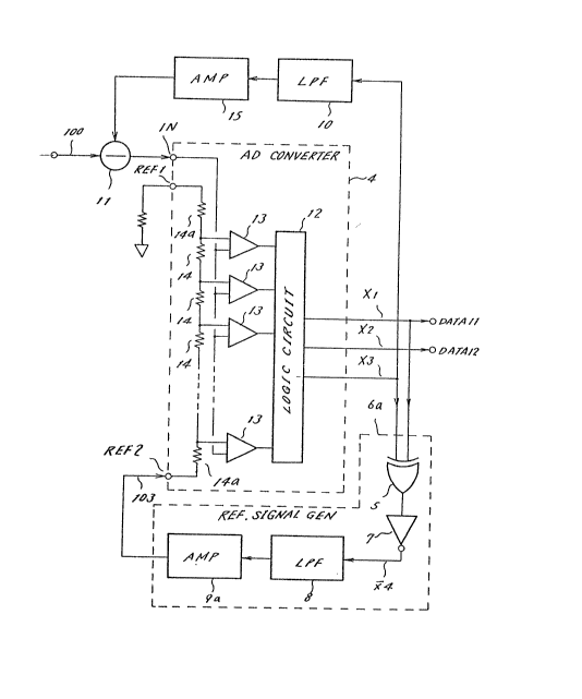
Referring now to Fig. 3, an automatic level control
cir~uit or an AD converter embodying the present invention
is shown. As shown, the circuit comprises an ~D converter
adapted to transform an input signal into 3-bit digital
signals by multi-level discrimination, and a reference
voltage generator 6 adapted to lbgically process the outputs
f~ 3' ~
-- 6 --
of the AD converter 4. The outputs of the reference
signal generator 6 are applied to the AD converter ~ to
control reference levels which are assigned to the AD
converter 4.
In detail, the AD converter 4 includes seven
comparators 13 to which the reference levels shown in
Fig. 2 are assigned. An input signal 100 (baseband
signal provided by QAM-detection of a 16-level QAM wave)
is applied -to an input terminal IN of the AD converter 4
and compared by the comparators 13 with the respective
reference levels. The outputs of the comparators 13 are
applied to a logic circuit 12 which then produces three-bit
output signals Xl, X2 and X3. The reference levels, or
voltages, associated with the respective comparators 13
are generated by dividing DC voltages applied to reference
voltage terminals REFl and REF2 of the AD converter 4
by means of a series connection of multiple voltage
di~iding resistors and 14a.
Among the outputs Xl - X3 of the AD converter 4, X
and X3 are applied to an Ex-OR gate 5 which is included
in the reference voltage generator 6. The output Oe the
Ex-OR gate 5 is delivered to an inverter 7 whose output
is coupled to an LPF 8. The LPF ~ separates a DC
component from the input and applies it to a polarity
converter 9 with the result that the DC component is
transformed into two reference voltages 101 and 102
~ . .
.
`
- 7 -
which are the same in level but opposite in polarity.
The reference voltages 101 and 102 respectively are
coupled to the reference voltage terminals REFl and REF2
of the AD converter 4.
In the construction described above, the output
X4' of the inverter 7 becomes a ONE when the level of
the input signal 100 has fluctuated to a level higher
than the reference level and becomes a ZERO when it has
fluctuated to a level lower than the reference level.
The positive and negative reference voltages applied to
the AD converter 4 increase responsive to a turn of the
signal X4l to a ONE so as to increase the distance
between each adjacent reference levels ~although the
center reference level i5 unchanged), while decreasing
it responsive to a turn of the signal X4' to a ZERO.
This allows the distance between the input level and
each reference.level to be successfully controlled to
an optimum one.
Referring to Fig~ 4, another.embodiment of the
preseht invention is shown. In this paxticular embodiment,
the automatic level control circuit comprises the AD
converter 4, a re~erence voltage generator 6a, a
subtractor 11 for applying subtraction to the input
signal 100, an LPF 10, and an amplifier 15.
In Fig. 4, the reference voltage generator 6a uses
an inverting amplifier 9a in place of the polarity
. ~
~;o~
-- 8
converter 9 of Fig. 3 so that a negative re~erence voltage
103 is applied to the reference voltage terminal REF2 o~
the AD converter 4. The other reference voltage terminal
REFl of the AD converter 4 is connected to ground via a
protective resistor. In such a circuit arrangement, a
change in the output of the reference voltage generator
6a causes not only the distance between adjacent reference
levels but also the center reference level to change.
To compensate for such an occurrence, the error signal
X3 output from AD converter 4 is routed to the subtractor
11 via the LPF 10 and amplifier 15.
The circuit in accordance with this particular
embodiment is capable of adjusting the distance between
adjacent re~erence levels to an optimum one responsive
to any fluctuation in the input level and, besides,
coping with drifts of a DC component which is superposed
on the input as well as DC drifts particular to the
circuit.
It should be noted that the DC component compensation
circuitry inclusi~e of the subtractor 11 as shown in
Fiy. 4 is applicable in the same manner to the arrangement
shown in Fig. 3. It should also be noted that the same
circuit arrangement is applicable to input signals other
than four-level signals. In an actual 16 Q~M demodulator,
the circuit of Fig. 3 or 4 will be directly connected
to each of the output components of the QAM detector 2
o~ Fi~. 1
Referring to Fig. 5, a 64 QAM demodulator is shown
which is made up of a QAM detector 40, 4-bit AD converters
41 and 42, reference signal generators 43 and 44, and a
carrier synchronizing circuit 45. The QAM detector 40
and the carrier synchronizing circuit 45 respectively
are constructed in the same manner as the circuits 2 and
21 of Fig. 1, while the reference signal generator 43
or 44 is constructed in the same manner as the circuit 6
of Fig. 3 or the circuit 6 of Fig. 4. The QAM detector 40
is adapted to detect a 64 QAM signal output from the
carrier synchronizing circuit 45 and, thereby, produce
quadrature slgnals P and Q. The.AD converter 41 converts
the output P of the QAM detector 40 to 4-bit digital
signals Xl - X4 responsive to reference voltages which
are applied thereto from the reference signal generator 43.
Among the signals Xl - X4, Xl - X3 are delivered as
reproduced data DATAll - DATA13, while the signal X4 is
applied to the reference signal ~enerator 43 together
with the signal Xl to be processecl in the same manner as
in FigO 3. Likewise, the AD converter 42 converts the
output Q of the QAM detector 40 to 4-bit digital signals
Yl - Y4 responsive to reference voltages which are applied
thereto from the reference signal generator 44. The
signals Yl ~ Y3 are delivered as reproduced data DATA21-23
while the signal Y4 is applied to the reference signal
generator 44 together with the signal Yl.
~æ~3f.~3~
-- 10 --
Referring to Fig. 6, another application of the
present inventlon to a 64 QAM demodulator is shown.
In Fig. 6, blocks 40, 42, 44 and 45 are the same as those
blocks of Fig. 5 which are designated by like reference
numerals, and blocks la, 5a and 20a those of Fig. 1.
In Fig. 6, fixed voltages are coupled to the terminals
REFl and REF2 of the AD converter 46, while outputs of
the reference signal generator 44 are coupled to those
of the AD converter 42 as has been the case with the
arrangement of Fig. 5. The automatic gain controlled
(AGC) circuit la which is connected to an input terminal
of the QAM detector 40 functions to compensate for the
level difference between the outputs P and Q of the
detector 40 only. Advantageous features of such a circuit
arrangement will be more clearly understood when compared
with the previously stated publication.
In summary, it will be seen that the present invention
provides an automatic level control circuit which is
capable of optimumly controlling the reference levels
of AD converters agalnst fluctuations of input level
without resortin~ to variable-~ain amplifiers, thereby
achieving a simple construction and promoting the ease
of adjustment.
Various modifications will become possible for those
skilled in the art after receiving the teachings of the
present disclosure without departing from the scope
thereo~.
. .