Language selection

Search

Patent 1263457 Summary

Third-party information liability

Some of the information on this Web page has been provided by external sources. The Government of Canada is not responsible for the accuracy, reliability or currency of the information supplied by external sources. Users wishing to rely upon this information should consult directly with the source of the information. Content provided by external sources is not subject to official languages, privacy and accessibility requirements.

Claims and Abstract availability

Any discrepancies in the text and image of the Claims and Abstract are due to differing posting times. Text of the Claims and Abstract are posted:

  • At the time the application is open to public inspection;
  • At the time of issue of the patent (grant).
(12) Patent: (11) CA 1263457
(21) Application Number: 1263457
(54) English Title: ARRANGEMENT FOR COUPLING HOLLOW WAVEGUIDES TO A SEMICONDUCTOR COMPONENT
(54) French Title: AGENCEMENT POUR L'ACCOUPLEMENT ENTRE GUIDES D'ONDES CREUX ET UN COMPOSANT SEMICONDUCTEUR
Status: Expired and beyond the Period of Reversal
Bibliographic Data
(51) International Patent Classification (IPC):
  • H01P 05/103 (2006.01)
(72) Inventors :
  • ALBERTY, MICHAEL (Germany)
  • GROSS, WALTER (Germany)
(73) Owners :
  • ANT NACHRICHTENTECHNIK G.M.B.H.
(71) Applicants :
  • ANT NACHRICHTENTECHNIK G.M.B.H. (Germany)
(74) Agent: SMART & BIGGAR LP
(74) Associate agent:
(45) Issued: 1989-11-28
(22) Filed Date: 1987-02-03
Availability of licence: N/A
Dedicated to the Public: N/A
(25) Language of filing: English

Patent Cooperation Treaty (PCT): No

(30) Application Priority Data:
Application No. Country/Territory Date
P 36 03 454.1 (Germany) 1986-02-05

Abstracts

English Abstract


ABSTRACT OF THE DISCLOSURE
An arrangement for coupling waveguide modes between two
waveguides via a semiconductor element. The two waveguides
each have a short-circuiting end wall and a common side wall
constituting a common partition wall between the waveguides
so that the two waveguides extend parallel to, and overlap
one another at least over a partial length where they are
separated from one another by the common side wall. The
common partition wall is provided with a coupling aperture
and the semiconductor element is inserted into the coupling
aperture between the two waveguides and is in ground contact
with the common partition wall. The semiconductor element
has two connecting arms, one connecting arm extending as a
coupling probe into one of the waveguides and the other
connecting arm extending as a coupling probe into the other
waveguide.


Claims

Note: Claims are shown in the official language in which they were submitted.


THE EMBODIMENTS OF THE INVENTION IN WHICH AN EXCLUSIVE
PROPERTY OR PRIVILEGE IS CLAIMED ARE DEFINED AS FOLLOWS:
1. In an arrangement for coupling waveguide modes
between two waveguides via a semiconductor element, wherein
the two waveguides have a common partition wall provided with
a coupling aperture, the semiconductor element is inserted
into the coupling aperture between the two waveguides, is in
ground contact with the common partition wall, and has two
connecting arms, one connecting arm extending as a coupling
probe into one of the waveguides and the other connecting arm
extending as a coupling probe into the other waveguide, the
improvement wherein:
said waveguides each have a short-circuiting end wall
and a common side wall constituting said common partition
wall so that said two waveguides extend parallel to, and
overlap one another at least over a partial length where they
are separated from one another by said common side wall.
2. Arrangement as defined in claim 1, wherein said
coupling aperture is inserted into said common side wall of
the two waveguides at a distance of .lambda./16 to .lambda./4 from a
respective one of said short-circuiting end walls, wherein
is the waveguide wavelength.
3. Arrangement as defined in claim 1, and further
including a dielectric substrate mounting said semiconductor
element, said semiconductor element having contact
terminals; two conductor paths extending in opposite
- 9 -

directions on said dielectric substrate and being connected
with the contact terminals of said semiconductor element; and
at least one conductive area disposed on said dielectric
substrate with which said semiconductor element is in ground
contact; wherein said dielectric substrate is disposed in
said coupling aperture with said at least one conductor area
connected with said common side wall and said conductor paths
each projecting as a said coupling probe into a respective
one of said two waveguides.
4. Arrangement as defined in claim 3, wherein said
waveguides each have a broad side and a narrow side and said
conductor paths each have a length which is 0.3 to 0.8 times
the length of the narrow side of the respective waveguide
into which it extends.
5. Arrangement as defined in claim 3, including wires
for supplying a direct voltage each being connected with a
respective one of said conductor paths, said wires each
extending perpendicularly to an E field of a respective one
of said waveguides.
6. Arrangement as defined in claim 1, including tuning
pins projecting into said waveguides through side walls of
said two waveguides and being disposed opposite said common
side wall in the vicinity of said coupling probes.
- 10 -

7. Arrangement as defined in claim 1, wherein said
waveguides each have a broad side and a narrow side and said
connecting arms each have a length of 0.3 to 0.8 times the
length of the narrow side of the respective waveguide into
which it extends.
8. Arrangement as defined in claim 1, including wires
for supplying a direct voltage each being connected with a
respective one of said connecting arms, said wires each
extending perpendicularly to an E field of a respective one
of said waveguides.
- 11 -

Description

Note: Descriptions are shown in the official language in which they were submitted.


63~57
BACKGROUND OF THE INVENTION
The present invention relates to an arrangement for
coupling waveguide modes between two waveguides via a
semiconductor element, with the semiconductor element being
inserted into a coupling aperture in a partition between the
two waveguides and being in ground contact with this parti-
tion. In such an arrangement the semiconductor element has
two connecting arms, one of which extends as a coupling probe
into one waveguide and the other of which extends as a
coupling probe into the other waveguide.
Such an arrangement is disclosed in a publication by
I. Angelov, A. Spasov, I. Stoev, L. Urshev, entitled "In-
vestigation of Some Guiding Structures For Low-Noise FET
Amplifiers", European Microwave Conference 1985, pages
535-540. This publication describes a high frequency
amplifier whose amplifier element is a field effect transis-
tor (FET). The FET is coupled in the manner described above
to an input waveguide and to an output waveguide, both being
disposed one behind the other along a common axis. This
known arrangement has a drawback in that its structural
length is unusually large, particularly if a multistage
amplifier is involved.
- 2 -

1263~57
SUMMARY OF THE INVENTION
It is an object of the present invention to provide
an arrangement of the above-mentioned type which has very
little attenuation and has the shortest possible structural
length.
The above and other objects are accomplished in the
context of an arrangement for coupling waveguide modes
between two waveguides via a semiconductor element as first
described above, wherein, according to the invention, the
waveguides each have a short-circuiting end wall and a common
side wall constituting the-common partition wall between the
waveguides so that the two waveguides extend parallel to, and
overlap one another at least over a partial length where they
are separated from one another by the common side wall.
Advantageously, in the arrangement according to the
invention, the connecting arms serving as coupling probes of
the semiconductor element may be very short. It is possible,
therefore, to permit very thin connecting arms to extend
freely into the waveguides without having to support them by
special means.
The overlap of input and output waveguides in the
coupling range according to the invention has the advantage
that it results in a considerable reduction of the str~ctural
Iength of the device, particularly in multistage high
- 3 -
~ ~ - ' " ' .
.
~:

1263457
freguency amplifiers, compared to comparable prior art
arrangements.
The invention will be described in greater detail below
with reference to an embodiment that is illustrated in the
drawings.
BRIEF DESCRIPTION OF THE DRAWINGS
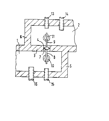
Figure 1 is a partial longitudinal sectional view of two
waveguides and a semiconductor element disposed therein
according to one embodiment of the invention.
Figure 2 is an end view into a waveguide arranged as
shown in Figure 1.
Figure 3 shows a similar arrangement as Figure 1, but
with the semiconductor element applied to a dielectric
substrate wafer.
Figure 4 is an end view into a waveguide arranged as
shown in Figure 3.
.
.

~263~S7
DESCRIPTION OF THE PREFERRED EMBODIMENTS
Figure 1 is a longitudinal sectional view of a microwave
circuit, e.g. an amplifier, oscillator, mixer or the like,
which includes an input waveguide and an output waveguide.
Input waveguide 1, which is short-circuited at its end wall
5, and output waveguide 2, likewise short-circuited at its
end wall 6, are parallel to one another over a length of
about A/8 to ~/2 (~ - waveguide wavelength) and are separated
from one another in a region of overlap by a common side
wall 3 on the broadside of the waveguides and common to both
waveguides in the overlap region. Input waveguide 1 is
coupled with output waveguide 2 by means of a coupling
aperture 4 provided in common side wall 3. This coupling
aperture 4 is spaced at about A/16 to ~/4 from the inner
surface of short-circuiting end wall 5 of input waveguide 1
and by the same distance from the inner surface of
short-circuiting end wall 6 of output waveguide 2.
An active semiconductor element 7 (e.g. a diode or an
FET) of the microwave circuit is inserted into coupling
aperture 4 between the two waveguides 1 and 2 and is in
ground contact with common side wall 3. A first connecting
arm 8 of semiconductor element 7 projects into input wave-
guide 1 and there couples into semiconductor element 7 the
mode of the input signal. A second connecting arm 9 of
semiconductor element 7 projects into output waveguide 2 and
~ ,.... -

~2634S~
couples into it the modes of the signal which have been, for
example, amplified or multiplied in frequency by the semi-
conductor element. Connecting arms 8 and 9, which serve as
coupling probes for semiconductor element 7, have a length
that is about 0.3 to 0.8 times the length of the narrow side
of the waveguide (i.e. about 0.15 to 0.35 cm at an operating
frequency of 20 GHz). Because this requires only very short
coupling probes, very thin and not very stable connecting
arms can project freely into waveguides 1 and 2, respectively,
and need no separate support.
Connecting arms 8 and 9 of semiconductor element 7 are
supplied with a direct voltage through coaxial feed-through 10
and 11 in the walls of waveguides 1 and 2, respectively. As
shown by the view into input waveguide 1 in Figure 2, the
direct voltage is fed to connecting arm 8 of semiconductor
element 7 through a thin wire 12 which passes through the
waveguide perpendicularly to the E field. This type of
direct voltage supply assures that the waveguide field is
inte-rfered with as little as possible and that the attenuation
during coupling is relatively low.
Matching the coupling between the waveguides and the
semiconductor element can be effected in a simple manner
by means of tuning screws 13, 14 and 15, 16, respectively,
which project into waveguides 1 and 2 through the waveguide
-- 6 --

~2~i3~57
walls opposite coupling aperture 4 in the vicinity of coupling
probes 8 and 9.
The arrangement shown in Figures 3 and 4 is identical
with the above-described arrangement of Figures 1 and 2 except
for the mounting of the semiconductor element and the configuration
of the coupling probes. Therefore, the same reference numerals
can be found in Figures 3 and 4 as are used in Figures l and 2.
In the embodiment shown in Figures 3 and 4, a semiconductor
element 7, which is not accommodated in a package, is placed
onto a dielectric substrate 17. At one side, substrate 17
is provided with two conductor paths 18 and l9 which each have
a length of about 0.3 to 0.8 times the length of the narrow
side of the waveguide and extend in opposite directions. Two
contact terminals of semiconductor element 7 are connected
with these conductor paths by means of bonding wires. Substrate
17 is provided with two further conductive areas 20a and 20b
with which the semiconductor element is grounded. This
dielectric substrate 17, equipped with semiconductor element 7,
is installed in coupling aperture 4 so that its conductive
areas 20a and 20b are contacted with common side wall 3 and
its conductor paths 18 and 19 project into waveguides 1 and 2
as coupling probes.
.~ :

1263~a57
27371-156
It will be understood that the above description of the
present invention is susceptible to various modifications, changes
and adaptations, and the same are intended to be comprehended
within the meaning and range of equivalents of the appended
claims.

Representative Drawing
A single figure which represents the drawing illustrating the invention.
Administrative Status

2024-08-01:As part of the Next Generation Patents (NGP) transition, the Canadian Patents Database (CPD) now contains a more detailed Event History, which replicates the Event Log of our new back-office solution.

Please note that "Inactive:" events refers to events no longer in use in our new back-office solution.

For a clearer understanding of the status of the application/patent presented on this page, the site Disclaimer , as well as the definitions for Patent , Event History , Maintenance Fee  and Payment History  should be consulted.

Event History

Description Date
Time Limit for Reversal Expired 1997-11-28
Letter Sent 1996-11-28
Grant by Issuance 1989-11-28

Abandonment History

There is no abandonment history.

Owners on Record

Note: Records showing the ownership history in alphabetical order.

Current Owners on Record
ANT NACHRICHTENTECHNIK G.M.B.H.
Past Owners on Record
MICHAEL ALBERTY
WALTER GROSS
Past Owners that do not appear in the "Owners on Record" listing will appear in other documentation within the application.
Documents

To view selected files, please enter reCAPTCHA code :


To view images, click a link in the Document Description column. To download the documents, select one or more checkboxes in the first column and then click the "Download Selected in PDF format (Zip Archive)" or the "Download Selected as Single PDF" button.

List of published and non-published patent-specific documents on the CPD .

If you have any difficulty accessing content, you can call the Client Service Centre at 1-866-997-1936 or send them an e-mail at CIPO Client Service Centre.


Document
Description 
Date
(yyyy-mm-dd) 
Number of pages   Size of Image (KB) 
Abstract 1993-09-14 1 20
Claims 1993-09-14 3 72
Drawings 1993-09-14 1 25
Descriptions 1993-09-14 7 167
Representative drawing 2001-04-25 1 7
Fees 1995-10-25 1 49
Fees 1994-10-17 1 43
Fees 1993-10-18 1 53
Fees 1992-10-18 1 36
Fees 1991-11-13 1 32