Sélection de la langue

Search

Sommaire du brevet 1263457 

Énoncé de désistement de responsabilité concernant l'information provenant de tiers

Une partie des informations de ce site Web a été fournie par des sources externes. Le gouvernement du Canada n'assume aucune responsabilité concernant la précision, l'actualité ou la fiabilité des informations fournies par les sources externes. Les utilisateurs qui désirent employer cette information devraient consulter directement la source des informations. Le contenu fourni par les sources externes n'est pas assujetti aux exigences sur les langues officielles, la protection des renseignements personnels et l'accessibilité.

Disponibilité de l'Abrégé et des Revendications

L'apparition de différences dans le texte et l'image des Revendications et de l'Abrégé dépend du moment auquel le document est publié. Les textes des Revendications et de l'Abrégé sont affichés :

  • lorsque la demande peut être examinée par le public;
  • lorsque le brevet est émis (délivrance).
(12) Brevet: (11) CA 1263457
(21) Numéro de la demande: 1263457
(54) Titre français: AGENCEMENT POUR L'ACCOUPLEMENT ENTRE GUIDES D'ONDES CREUX ET UN COMPOSANT SEMICONDUCTEUR
(54) Titre anglais: ARRANGEMENT FOR COUPLING HOLLOW WAVEGUIDES TO A SEMICONDUCTOR COMPONENT
Statut: Périmé et au-delà du délai pour l’annulation
Données bibliographiques
(51) Classification internationale des brevets (CIB):
  • H01P 05/103 (2006.01)
(72) Inventeurs :
  • ALBERTY, MICHAEL (Allemagne)
  • GROSS, WALTER (Allemagne)
(73) Titulaires :
  • ANT NACHRICHTENTECHNIK G.M.B.H.
(71) Demandeurs :
  • ANT NACHRICHTENTECHNIK G.M.B.H. (Allemagne)
(74) Agent: SMART & BIGGAR LP
(74) Co-agent:
(45) Délivré: 1989-11-28
(22) Date de dépôt: 1987-02-03
Licence disponible: S.O.
Cédé au domaine public: S.O.
(25) Langue des documents déposés: Anglais

Traité de coopération en matière de brevets (PCT): Non

(30) Données de priorité de la demande:
Numéro de la demande Pays / territoire Date
P 36 03 454.1 (Allemagne) 1986-02-05

Abrégés

Abrégé anglais


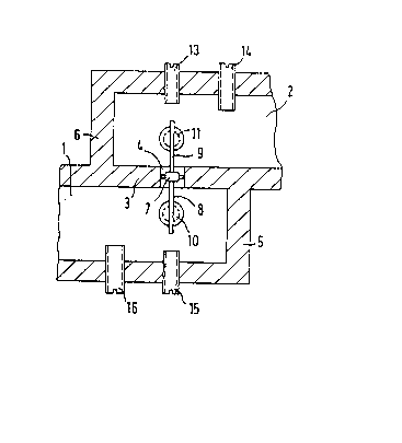
ABSTRACT OF THE DISCLOSURE
An arrangement for coupling waveguide modes between two
waveguides via a semiconductor element. The two waveguides
each have a short-circuiting end wall and a common side wall
constituting a common partition wall between the waveguides
so that the two waveguides extend parallel to, and overlap
one another at least over a partial length where they are
separated from one another by the common side wall. The
common partition wall is provided with a coupling aperture
and the semiconductor element is inserted into the coupling
aperture between the two waveguides and is in ground contact
with the common partition wall. The semiconductor element
has two connecting arms, one connecting arm extending as a
coupling probe into one of the waveguides and the other
connecting arm extending as a coupling probe into the other
waveguide.

Revendications

Note : Les revendications sont présentées dans la langue officielle dans laquelle elles ont été soumises.


THE EMBODIMENTS OF THE INVENTION IN WHICH AN EXCLUSIVE
PROPERTY OR PRIVILEGE IS CLAIMED ARE DEFINED AS FOLLOWS:
1. In an arrangement for coupling waveguide modes
between two waveguides via a semiconductor element, wherein
the two waveguides have a common partition wall provided with
a coupling aperture, the semiconductor element is inserted
into the coupling aperture between the two waveguides, is in
ground contact with the common partition wall, and has two
connecting arms, one connecting arm extending as a coupling
probe into one of the waveguides and the other connecting arm
extending as a coupling probe into the other waveguide, the
improvement wherein:
said waveguides each have a short-circuiting end wall
and a common side wall constituting said common partition
wall so that said two waveguides extend parallel to, and
overlap one another at least over a partial length where they
are separated from one another by said common side wall.
2. Arrangement as defined in claim 1, wherein said
coupling aperture is inserted into said common side wall of
the two waveguides at a distance of .lambda./16 to .lambda./4 from a
respective one of said short-circuiting end walls, wherein
is the waveguide wavelength.
3. Arrangement as defined in claim 1, and further
including a dielectric substrate mounting said semiconductor
element, said semiconductor element having contact
terminals; two conductor paths extending in opposite
- 9 -

directions on said dielectric substrate and being connected
with the contact terminals of said semiconductor element; and
at least one conductive area disposed on said dielectric
substrate with which said semiconductor element is in ground
contact; wherein said dielectric substrate is disposed in
said coupling aperture with said at least one conductor area
connected with said common side wall and said conductor paths
each projecting as a said coupling probe into a respective
one of said two waveguides.
4. Arrangement as defined in claim 3, wherein said
waveguides each have a broad side and a narrow side and said
conductor paths each have a length which is 0.3 to 0.8 times
the length of the narrow side of the respective waveguide
into which it extends.
5. Arrangement as defined in claim 3, including wires
for supplying a direct voltage each being connected with a
respective one of said conductor paths, said wires each
extending perpendicularly to an E field of a respective one
of said waveguides.
6. Arrangement as defined in claim 1, including tuning
pins projecting into said waveguides through side walls of
said two waveguides and being disposed opposite said common
side wall in the vicinity of said coupling probes.
- 10 -

7. Arrangement as defined in claim 1, wherein said
waveguides each have a broad side and a narrow side and said
connecting arms each have a length of 0.3 to 0.8 times the
length of the narrow side of the respective waveguide into
which it extends.
8. Arrangement as defined in claim 1, including wires
for supplying a direct voltage each being connected with a
respective one of said connecting arms, said wires each
extending perpendicularly to an E field of a respective one
of said waveguides.
- 11 -

Description

Note : Les descriptions sont présentées dans la langue officielle dans laquelle elles ont été soumises.


63~57
BACKGROUND OF THE INVENTION
The present invention relates to an arrangement for
coupling waveguide modes between two waveguides via a
semiconductor element, with the semiconductor element being
inserted into a coupling aperture in a partition between the
two waveguides and being in ground contact with this parti-
tion. In such an arrangement the semiconductor element has
two connecting arms, one of which extends as a coupling probe
into one waveguide and the other of which extends as a
coupling probe into the other waveguide.
Such an arrangement is disclosed in a publication by
I. Angelov, A. Spasov, I. Stoev, L. Urshev, entitled "In-
vestigation of Some Guiding Structures For Low-Noise FET
Amplifiers", European Microwave Conference 1985, pages
535-540. This publication describes a high frequency
amplifier whose amplifier element is a field effect transis-
tor (FET). The FET is coupled in the manner described above
to an input waveguide and to an output waveguide, both being
disposed one behind the other along a common axis. This
known arrangement has a drawback in that its structural
length is unusually large, particularly if a multistage
amplifier is involved.
- 2 -

1263~57
SUMMARY OF THE INVENTION
It is an object of the present invention to provide
an arrangement of the above-mentioned type which has very
little attenuation and has the shortest possible structural
length.
The above and other objects are accomplished in the
context of an arrangement for coupling waveguide modes
between two waveguides via a semiconductor element as first
described above, wherein, according to the invention, the
waveguides each have a short-circuiting end wall and a common
side wall constituting the-common partition wall between the
waveguides so that the two waveguides extend parallel to, and
overlap one another at least over a partial length where they
are separated from one another by the common side wall.
Advantageously, in the arrangement according to the
invention, the connecting arms serving as coupling probes of
the semiconductor element may be very short. It is possible,
therefore, to permit very thin connecting arms to extend
freely into the waveguides without having to support them by
special means.
The overlap of input and output waveguides in the
coupling range according to the invention has the advantage
that it results in a considerable reduction of the str~ctural
Iength of the device, particularly in multistage high
- 3 -
~ ~ - ' " ' .
.
~:

1263457
freguency amplifiers, compared to comparable prior art
arrangements.
The invention will be described in greater detail below
with reference to an embodiment that is illustrated in the
drawings.
BRIEF DESCRIPTION OF THE DRAWINGS
Figure 1 is a partial longitudinal sectional view of two
waveguides and a semiconductor element disposed therein
according to one embodiment of the invention.
Figure 2 is an end view into a waveguide arranged as
shown in Figure 1.
Figure 3 shows a similar arrangement as Figure 1, but
with the semiconductor element applied to a dielectric
substrate wafer.
Figure 4 is an end view into a waveguide arranged as
shown in Figure 3.
.
.

~263~S7
DESCRIPTION OF THE PREFERRED EMBODIMENTS
Figure 1 is a longitudinal sectional view of a microwave
circuit, e.g. an amplifier, oscillator, mixer or the like,
which includes an input waveguide and an output waveguide.
Input waveguide 1, which is short-circuited at its end wall
5, and output waveguide 2, likewise short-circuited at its
end wall 6, are parallel to one another over a length of
about A/8 to ~/2 (~ - waveguide wavelength) and are separated
from one another in a region of overlap by a common side
wall 3 on the broadside of the waveguides and common to both
waveguides in the overlap region. Input waveguide 1 is
coupled with output waveguide 2 by means of a coupling
aperture 4 provided in common side wall 3. This coupling
aperture 4 is spaced at about A/16 to ~/4 from the inner
surface of short-circuiting end wall 5 of input waveguide 1
and by the same distance from the inner surface of
short-circuiting end wall 6 of output waveguide 2.
An active semiconductor element 7 (e.g. a diode or an
FET) of the microwave circuit is inserted into coupling
aperture 4 between the two waveguides 1 and 2 and is in
ground contact with common side wall 3. A first connecting
arm 8 of semiconductor element 7 projects into input wave-
guide 1 and there couples into semiconductor element 7 the
mode of the input signal. A second connecting arm 9 of
semiconductor element 7 projects into output waveguide 2 and
~ ,.... -

~2634S~
couples into it the modes of the signal which have been, for
example, amplified or multiplied in frequency by the semi-
conductor element. Connecting arms 8 and 9, which serve as
coupling probes for semiconductor element 7, have a length
that is about 0.3 to 0.8 times the length of the narrow side
of the waveguide (i.e. about 0.15 to 0.35 cm at an operating
frequency of 20 GHz). Because this requires only very short
coupling probes, very thin and not very stable connecting
arms can project freely into waveguides 1 and 2, respectively,
and need no separate support.
Connecting arms 8 and 9 of semiconductor element 7 are
supplied with a direct voltage through coaxial feed-through 10
and 11 in the walls of waveguides 1 and 2, respectively. As
shown by the view into input waveguide 1 in Figure 2, the
direct voltage is fed to connecting arm 8 of semiconductor
element 7 through a thin wire 12 which passes through the
waveguide perpendicularly to the E field. This type of
direct voltage supply assures that the waveguide field is
inte-rfered with as little as possible and that the attenuation
during coupling is relatively low.
Matching the coupling between the waveguides and the
semiconductor element can be effected in a simple manner
by means of tuning screws 13, 14 and 15, 16, respectively,
which project into waveguides 1 and 2 through the waveguide
-- 6 --

~2~i3~57
walls opposite coupling aperture 4 in the vicinity of coupling
probes 8 and 9.
The arrangement shown in Figures 3 and 4 is identical
with the above-described arrangement of Figures 1 and 2 except
for the mounting of the semiconductor element and the configuration
of the coupling probes. Therefore, the same reference numerals
can be found in Figures 3 and 4 as are used in Figures l and 2.
In the embodiment shown in Figures 3 and 4, a semiconductor
element 7, which is not accommodated in a package, is placed
onto a dielectric substrate 17. At one side, substrate 17
is provided with two conductor paths 18 and l9 which each have
a length of about 0.3 to 0.8 times the length of the narrow
side of the waveguide and extend in opposite directions. Two
contact terminals of semiconductor element 7 are connected
with these conductor paths by means of bonding wires. Substrate
17 is provided with two further conductive areas 20a and 20b
with which the semiconductor element is grounded. This
dielectric substrate 17, equipped with semiconductor element 7,
is installed in coupling aperture 4 so that its conductive
areas 20a and 20b are contacted with common side wall 3 and
its conductor paths 18 and 19 project into waveguides 1 and 2
as coupling probes.
.~ :

1263~a57
27371-156
It will be understood that the above description of the
present invention is susceptible to various modifications, changes
and adaptations, and the same are intended to be comprehended
within the meaning and range of equivalents of the appended
claims.

Dessin représentatif
Une figure unique qui représente un dessin illustrant l'invention.
États administratifs

2024-08-01 : Dans le cadre de la transition vers les Brevets de nouvelle génération (BNG), la base de données sur les brevets canadiens (BDBC) contient désormais un Historique d'événement plus détaillé, qui reproduit le Journal des événements de notre nouvelle solution interne.

Veuillez noter que les événements débutant par « Inactive : » se réfèrent à des événements qui ne sont plus utilisés dans notre nouvelle solution interne.

Pour une meilleure compréhension de l'état de la demande ou brevet qui figure sur cette page, la rubrique Mise en garde , et les descriptions de Brevet , Historique d'événement , Taxes périodiques et Historique des paiements devraient être consultées.

Historique d'événement

Description Date
Le délai pour l'annulation est expiré 1997-11-28
Lettre envoyée 1996-11-28
Accordé par délivrance 1989-11-28

Historique d'abandonnement

Il n'y a pas d'historique d'abandonnement

Titulaires au dossier

Les titulaires actuels et antérieures au dossier sont affichés en ordre alphabétique.

Titulaires actuels au dossier
ANT NACHRICHTENTECHNIK G.M.B.H.
Titulaires antérieures au dossier
MICHAEL ALBERTY
WALTER GROSS
Les propriétaires antérieurs qui ne figurent pas dans la liste des « Propriétaires au dossier » apparaîtront dans d'autres documents au dossier.
Documents

Pour visionner les fichiers sélectionnés, entrer le code reCAPTCHA :


Pour visualiser une image, cliquer sur un lien dans la colonne description du document. Pour télécharger l'image (les images), cliquer l'une ou plusieurs cases à cocher dans la première colonne et ensuite cliquer sur le bouton "Télécharger sélection en format PDF (archive Zip)" ou le bouton "Télécharger sélection (en un fichier PDF fusionné)".

Liste des documents de brevet publiés et non publiés sur la BDBC .

Si vous avez des difficultés à accéder au contenu, veuillez communiquer avec le Centre de services à la clientèle au 1-866-997-1936, ou envoyer un courriel au Centre de service à la clientèle de l'OPIC.


Description du
Document 
Date
(aaaa-mm-jj) 
Nombre de pages   Taille de l'image (Ko) 
Abrégé 1993-09-14 1 20
Revendications 1993-09-14 3 72
Dessins 1993-09-14 1 25
Description 1993-09-14 7 167
Dessin représentatif 2001-04-25 1 7
Taxes 1995-10-25 1 49
Taxes 1994-10-17 1 43
Taxes 1993-10-18 1 53
Taxes 1992-10-18 1 36
Taxes 1991-11-13 1 32