Note: Descriptions are shown in the official language in which they were submitted.
5~'~
RECO~DING ELEMENTS COMPRISING
WRITE-ONCE THIN FILM ~LLOY L~YERS
Field of the Inuention
This inuention relates to recording elem~nts
and recording methods.
B~CKGROUND OF THE INUENTION
Thin film optical recording layers using
chalcogenide thin-films and amorphous to crystalline
phase transitions haue been the subject of many
in~estigations since the early 1970's. The initial
10 interests were focused on "erasable", and therefore
reusable, optical recording layers since the amor-
phous to crystalline transition ls, in principle, a
re~ersible process. Such layers are generally pre-
pared by a uacuum process. The layer is amorphous
15 when so prepared. ~ low power, relati~ely long
duration laser pulse is used to heat a local spot on
the layer to below the melting point for a sufficient
length of time to cause the spot to crystallize.
These crystalline spots can in turn be heated, by a
20 higher power, shorter duration laser, abo~e the
melting point of the crystallized spots to randomize
the structure of the spots. The layer is designed
such that upon the termination of the laser pulse the
cooling rate of the heated spot is high ~nough that
the randomi7ed structure is frozen to achieue an
amorphous state.
Thus by adiusting the laser power and
d~ration, the state of a selected area on the layer
can be switched between the amorphous state and the
30 crystalline state to create a pattern of amorphous
and crystalline spots which can be used for informa-
tion storage. Since the phase transition is
reuersible, the pattern can be erased and replaced
with a different recorded pattern. Theoretically,
35 this erase-write cycle can be carried out any number
of times.
35~
_~_
~ principal difficulty is that the rate of
crystallization of most layers studied is wsually too
low. For practical applications, it is desirable to
ha~e layers which can be crystallized by laser pulses
shorter than a microsecond (~s). Presently, few
materials ha~e demonstrated such capabilities. For
some materials with high crystallization rates (e.g.
Te-Sn alloy), the data retention times are often not
adequate because of the instability of the amorphous
state.
Because of the slow crystallization of most
materials, the crystallization step is generally used
as the erasure step in erasable optical recording
layers. ~ laser spot elongated in the direction of
the laser mo~ement is used to giue an effecti~ely
long duration laser exposure. Such long laser spots
cannot be used for high density recordings. The
amorphizing step, on the other hand, is used as the
recording step since this can be achieved with short
laser pulse, and hence can be done at high speed.
Uery few materials are known for optical
recording layers in which the abo~e described write-
erase-write cycle is of practical use. No erasable
phase-change type optical recording layers haue beçn
commerclalized.
~ good deal of attention has also focused on
so-called "write-once" thin film optical recording
layers. Write-once simply means that the layers can
be recorded upon only once. Such layers cannot be
erased and reused for a subsequent recording.
Since thin film optical recording layers are
generally amorphous when prepared, it is desirable to
use the crystallization step as the recording step in
write-once layers. Howe~er, the problem of slow
crystallization pre~ents the achie~ement of high data
539~
--3--
rates. High data rates are critical for write-once
layers designed fQr use with computers.~
European Patent ~pplication 0184452 broadly
discloses erasable optical recording layers of
antimony and germanium. No instructions are giuen
regarding what the relati~e proportion of ~ach
element should be in the layers. ~lso no examples
are giuen of antimony and germanium layers. Informa-
tion recording and erasure are said to be achie~ed by
switching the layers between two different crystal-
line states. The layers are generally prepared in
the amorphous states which ha~e to be first con~erted
into one of the two crystalline states before
information can be recorded. The crystalli~ation
step, achie~ed by either a bulk heat-treatment or a
prolonged laser exposure, is sa~d to have a lower
reflectance than the amorphous state. Exa~ples of
antimony and germanium alloys were not giuen and the
examples of alloys other than antimony and gerrnanium
are disclosed. Layers of such alloys ha~e a uery low
rate of crystalli~ation. This application further
teaches that the optical recording layers disclosed
therein are unsuitable for use in the amorphous-to-
crystalline transition mechanism because of the
instability of the amorphous state in generAl.
Experimental e~idence has shown that the
crystallin2-crystalline recordings and the fast
amorphous-to-crystalline recordings are mutually
exclusiue. Compositions which demonstrate properties
suitable for one mode of recording are not suitable
for the other mode of recording.
~ nother problem is that many of the
chalcogen containing materials which undergo the
amorphous-to-crystalline transition mechanism are
usually corrosion prone.
1~ 534
The problem is that the prior art has not
provided writc-once optical recording layers which
possess the combination of a) a crystalli~ation rate
less than l.O ~s~ b) good corrosion resistance, c)
a stable amorphous state and d) a capability of high
rate, high density recordings.
BRIEF DESCRIPTION OF THE DRAWINGS
Figure 1 is a description of a schematic
recording and readback apparatus for using the
recording elements of the invention; and
Figure 2 is a schematic cross section of an
optical recording element of this invention; and
Figures 3 and 4 are curves showing some of
the experimental results of examples 1 and 3.
Figure 5 is a ternary composition diagram
showing polygons within which useful alloy mixtures
of the present invention are found.
SUMMARY OF THE INVENTION
The present invention provides a recording
element comprising a write-once amorphous thin-film
optical recording layer of an alloy having a composi-
tion within a polygon in a ternary composition
diagram of antimony, tin and germanium described in
figure 5 herein; wherein the polygon has the follow-
ing vertices and corresponding coordinates in atompercent:
Vertices Coordinates
Sb Sn Ge
A 86 13.990.01
B 55 44.990.01
C 18 52 30
D 18 42 40
78 o 22
F 98 0 2
}53~
-5-
The present invention also provides a record
element having
a) a composition within the above described
polygon in figure 5; and
b) a pattern of amorphous and crystalline areas
in which the crystalline areas are all in the same
state with a higher reflectivity than the amorphous
state.
The elements of this invention do not suffer
the environmental corrosion seen in chalcogen rich
thin films. The rate of crystallization of the
optical recording layers is less than 1 ~s using
p~actical laser power. The amorphous state is very
stable. Thus, recordings on the thin film are made
15 using the amorphous to crystalline transition
mechanism~ The layers are capable of high denslty,
high rate recordings. Moreover the layers cannot be
switched between two different crystalline states as
suggested by European Patent Application 0184452 and
the crystalline state is uniformly more reflective
than the amorphous state.
It has been found that layers formed rom
alloy compositions outside of the defined polygon a)
are either crystalline as deposited or b) crystallize
too slowly to be of practical use. The layers have
an amorphous to crystalline transition temperature of
at least 80OC.
Layers used in the elements of the invention
are capable of forming only a single crystalline
state. That is the crystalline state is the same
throughout the recorded layer. In many recordings
the crystalline areas will have a uniform composition.
Especially useful record and recording
elements have alloy compositions within the polygon
in figure 5 having the following vertices and
corresponding coordinates:
~3~3~
-6-
Vert ce~ ~s~ordinates
Sb Sn Ge
A 86 13.990.01
B 55 44.990.01
C 18 52 30
D 18 42 40
I 75 2 23
J 96 2 2
Preferred record and recording elements have
alloy compositions with the polygon of figure 5
having the following vertices and corresponding
coordinates:
Vertices Coordinates
~ Sn Ge
A 86 13.990.01
B 55 44.990.01
G 40 48 12
36 24
DETAILED DESCRIPTION OF THE I~VENTIOM
Recording information on the thin film
layers is achieved by focusing an information modu-
lated laser beam on the layer thereby forming a
pattern of crystalline and amorphous areas on the
layer. All the crystalline areas will be in the same
3~ state.
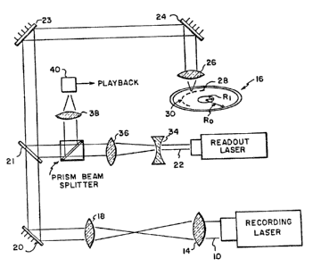
Figure 1 shows a schematic of an apparatus
for recording information on an optical recording
element 16 of the invention and for playing back the
recorded information therefrom. Referring to-
~i~
~Z6353~
figure 2, recording element 16 comprises an o~ercoatlayer 41, amorphous thin film optical recording layer
42 on substrate 45. In response to a dri~e signal,
the intensity of a diode recording beam is modulated
in accordance with information to be recorded on thin
film 42. The modulated laser be~m is collected by a
lens 14 and collimated by a lens 18 and is directed
by means of mirror elements 20, 23 and 24 to a lens
26 which focuses the modulated laser beam to a
recording spot 28 on the film 42 as shown in fiywre 1.
During recording, the element 16 is spun at
a constant rate, e.g. 1800 rotations per minute
(rpm~. ~s a result, a track of information 30 is
recorded on the optical recording layer in the form
of selected crystallized areas. ~s recording contin-
ues, the recording spot 28 is caused (by means not
shown) to scan radially in~ard across the element 16,
thereby causing information to be recorded along a
spiral or concentric track that extends from an outer
radius rO to an inner radi~s ri. The sizes and
spacings of the recorded information marks uary in
accordance with the information content of the
recording laser dri~e signal, as well as with radial
position on the element 16.
During the readback process, the new
information bearing element 16 is spun at the same
rate as it was spun during the recording process. Q
laser beam 22 from a readout laser is e~panded in
diameter by means of lenses 34 and 36. The optical
path of the readout laser beam is folded by a beam
splitter 21 and mirrors 23 and 24 so that the readout
laser beam is focused to a playback spot on the
element 16 by the high numerical aperture lens 26.
The element 16 is assumed to be of the refle~ti~e
type so that the radiation forming the playback spot
534
-8-
is reflected b~ck through the high numerical aperture
lens 26 after interacting with the information rnarks
recorde~ on the optical element 16. A lens 38
directs reflected laser radiation which has been
di~erted by the prism beamsplitter onto a detector 40
which produces an electrical playback signal in
response to temporal variations ~contrast) in the
irradiance of the reflected laser radiation falling
on the detector,
The amorphous thin film optical recording
layers of this in~ention are written upon with a
coherent beam of electromagnetic radiation of suffi-
cient energy to con~ert selected portions of the
amorphous film 42 to a crystalline state. In the
present inuention the amorphous thin film optical
recording layers are of sufficient sensitiuity that
-laser powers of about 2 to 10 mW at laser pulsewidth
of 40 to 100 nanoseconds pro~ides sufficient energy
to make the conuersion.
Recorclings on the amorphous thin film were
made with a static pit tester.
The static pit tester pro~ides automated
facilities in which a microcomputer controls the
sample position, the laser power and the laser pulse-
width. Each recording layer is exposed with a 830
nanometer laser diode in the static pit tester to
produce a matrix of spots in which the laser power is
varied from 4 to 12 mW and the pulse width ~aried
from 40 to 30,000 nanoseconds. The suitability of
the recording layer for optical recording is deter-
mined by measuring the change in reflection between
the exposed and unexposed areas of the sample, i.e.
between the crystalline and amorphous states.
This reflection change is expressed as
recording contrast, CT, by the following definition:
~Z~353~
_g_
R - R
CT - Rc ~ Ra
wherein Rc and Ra are the reflectances of the
crystalline and the amorphous states, respectiuely.
minimum contrast of 5 percent must be achie~ed for the
films to be considered use~ul as optical recording
layers.
The thin amorphous film recording layers san
be prepared by con~entional thin film deposition
techniques such as e~aporation, Rf (radio frequency)
and DC ~direct current) sputtering from an alloy
target, and RF and DC co-sputtering from targets of
the indi~idual elements. Enhancement of sputtering
processes by applying magnetic fields (magnetron
sputtering) can also be used. The thickness of the
films can be from a few tens to a few hundreds nano-
meters depending on compromises among factors such as
contrast, sensiti~ity, production rate, material cost,
ease of control" data rate, etc.
Supports which ean be used include plastic
films, such as polyethylene terephthalate, polymethyl
methacrylate, and polycarbonate, a glass plate, paper
and metallic plates.
The practice of the in~ention is further
described in the following examples. In the examples,
each thin film optical recording layer is represented
by the symbol SbxGey5nz wherein x, y and z are
atom percents.
Example 1
Amorphous thin film optical recording layers
of this in~ention were prepared ky a sp~ttering
process. ~ target composed of homogeneously mixed Sb
and Ge powders was pre-sputtered in an 8 mtorr ~r
:~L r ~ ~ ~ r3 ~3 9L
--1~
atmosphere for one hour. The pre sputtering step was
designed to achieue a steady state deposition
condition.
Thin films of about 140 nm in thickn~ss were
then prepared by sputtering the pre-sputtered mix for
7 minutes onto a glass support. The atomic fraction
of each component in the prepared film was determined
by inducti~ely coupled plasma atomic emission
spectrometry (ICP) and X-ray florescence (XRF). The
recording layer comprised 91.5% Sb and B.5% Ge. The
amorphous to crystalline transition temperature was
164~C. This high transition temperature shows that
the amorphous state of the films of the invention are
uery stable. This is an important keeping property.
~ ~ery low transition temperature from amorphous to
crystalline would be detrimental to optical recording
layers in that the reflectance difference between
written data encoded as crystalline marks and unmarked
amorphous areas would be lost.
~nother sample of the above film was written
upon using the static pit tester described herein
before. The writing was in the form of crystalli~ed
marks on the films. The film with the crystallized
written spots was placed in a chamber at 70~C and 30
percent relative humidity for an accelerated stability
test. ~fter 44 days, the film was examined. We did
not obser~e any phase change or corrosion on the
unwritten film or the written spots. The film did not
ha~e any overcoat as a protecti~e layer against
corrosion. This test shows that the films of the
~in~ention hearing written spots are also en~ironmen-
tally stable.
~ nother film sample of the same composition
was subjected to performance tests on the static pit
tester. The film was o~ercoated with a ~acuum coated
:
:
1~3S3~
-Il-
140 nm thick SiO2 film to reduce deformation during
the writing step ~ pulsed semiconductor laser beam
with a wauelength of 830 nm was used for writing. The
writing sensiti~ity and contrast at various powers and
5 pulse widths are shown in Figure 3. Figure 3 shows
that the percent contrast between the reflectance of
the amorphous state and the reflectance of the crys-
tallized state is clearly measurable and can thus be
read by state of the art laser read systems. These
data also show that the thin films can be written upon
using practical laser powers and writing speeds.
Example 2
~ number of amorphous Sb-Ge thin films with a
range of compositions were prepared according to the
method in Example l. Some of the representati~e
compositions and their corresponding writing sensiti~-
ities (minimum required laser pulse length and power)
are listed in the following: Sbg4Ge6, 50 ns,
6 mW; Sb89Gel1, 100 ns, 6 mW; Sb86Gel4,
200 ns, 8 mW; Sb84Gel6, 400 ns 8 mW; Sb79Ge21,
1 ~s, 10 mW.
The thin films of examples 1 and 2 are sensi-
tive write-once optical recording layers. The films
cannot be cycled between two different crystalline
states as taught in European Patent ~ppli~ation
0184452.
Example 3
~morphous thin film optical recording layers
of this in~ention were prepared by the sp~ttering
process of example l.
Thin films of about 100 nm in thickness were
then prepared by sputtering the pre-sputtered mix for
4 minutes onto a glass support. The atomic fraction
3~
-12-
of each component in the prepared film was determined
by ICP. The composition of the film on an atom to
atom basis was 64% Sb, 30% Sn and 6% Ge.
The amorphous to crystalline transition
temperature was 152C as shown in Figure 4. The
heating rate was 25 milli-Kel~in per second.
This high transition temperature shows that
the amorphous state of the films of this in~ention are
~ery stable.
hnother sample of the abo~e thin film was
written upon using the static pit tester clescribed
herein before~ The writing was in the form of crys-
tallized marks on the film. The film with the
crystallized written spots was placed in a chamber at
70~C and 30 percent relati~e humidity for an acceler-
ated stability test. ~fter 24 days, the film was
examined. We did not obser~e any phase change or
corrosion on thl3 unwritten film or the written spots.
This test shows that the films of the in~ention
bearing written spots are also en~ironmentally stable.
~ nother film sample of the same composition
was subjected to performance tests on a static pit
tester. ~ pulsed semiconductor laser beam with a
wa~elength of 830 nm was wsed for writing. The
resulting data showed that the thin ~ilms can be
written upon using practical laser powers and writing
speeds. The writing contrast was about 20 percent at
a pulse width of 100 ns and 10 mW of laser power. The
sensiti~ity of the film was such that it could be
written upon at 40 ns and 4 mW of power.
Example 4
A number of amorphous Sb-Ge-Sn thin films
with a range of compositions were prepared according
to the method of Example 1. Some of the representati~e
53~
-13-
compositions are Sb81Ge~Snl4, Sb78Ge8Sn14,
7~ 4 24~ sb6sGe7sn24~ Sbfi6Ge4sn30and Sb65~e9sn26
These films can be written upon at a laser pulse
length of 50 ns and power of 6 mW. The written
information was in the form of crystalline spots.
Example 5
~ homogeneous Sb-Ge-Sn alloy sputtering
target was prepared by hot pressing. ~n amorphous
thin film, with a composition of Sb74Ge4Sn22,
was prepared by sputtering. The film can be crystal-
lized at a laser pulse length of S0 ns and power of
4 mW.
Comparatiue Example
Thin films were prepared in which the alloy
compositions were 1) Sb40Sn58Ge2 and 2)
Sb58Sn2Ge40. Thin film 1) was crystalline when
deposited. Thin film 2) was amorphous when deposited
but extremely difficult to crystallize. 80th of these
films are outside oF the scope of the present
in~ention.
The in~ention has been described in detail
with particular reference to preferred embodiments
thereof, but it will be understood that variations and
modifications can be effected within the spirit and
scope of the invention.
3~