Note: Descriptions are shown in the official language in which they were submitted.
1~37~;~
Preformatted information medium and optical reader device.
FIELD OF THE INVENTION
The present invention relates to optical memories for
storing data in reserved areas on the surface of an information
medium. In order to provide fast and easy access to data
areas, this type of information medium may be in the form of a
disk whose reference surface is split up into regularly spaced
track elements. These track elements may, for example, follow
the path of spiral turns in a constant pitch spiral which is
centered on the center of a centering orifice. The data areas
may also be subdivided angularly into sectors, and the sectors
may be subdivided into blocks for containing data and for
containing the addresses which are essential for addressing
track elements and sectors. By virtue of this radial and
angular distribution o~ data areas, the handling of data
transcription can be particularly flexible using a read/write
head which is displaceable radially over the reference surface
of the disk either to follow a track element regularly, or else
to skip quickly over the distance separating any two track
elements. Which sector or data block is selected depends on
disk rotation, and in general this is fast enough to ensure a
high data rate. In order to locate specific track elements and
the portions thereof which are allocated to data storage, the
reference surface of the disk is "formatted", i.e. it is marked
with prerecorded reference ma~ks which are interspersed between
the data areas. A light spot can be constrained to center
itself exactly on the axis of a track, in spite of any possible
excentricity defects of the disk by making use of the
repetitive nature of these reference marks. Some of the
reference marks are made from prerecorded patterns which are
specifically intended for synchronizing a clock which governs
the serial spacing of the data and of the other reference marks
scanned by the light spot.
The reference surface of an optical memory has a change in
its optical characteristics at the locations of the prerecorded
patterns, and this change is detected by a verv fine light
spot. Tracking errors and losses of synchronization which need
1;2637S~-O
to be compensated can thus readily be detected by optically
scanning the disk. Other modifications of the optical
characteristics are produced by writing data, but steps are
taken to ensure that such data writing or "postrecording" does
not effect the prerecorded patterns necessary for tracking and
for clock s~nchroni~ation.
The use of an optical memory such as a preformatted
optical disk requires an optical reader device which includes:
means for projecting as small as possible a light spot onto the
reference surface of the disk; means for radially displacing
said spot; photodetector means for detecting radiation which
has interacted optically and has been returned from the illum-
inated region of the reference surface; and means for causing
the disk to rotate. When using high inormation density
optical disks, it is essential to provide radial servocontrol
of the spot position together with automatic spot focusingO
Finally, in order to write information on the disk, it is
necessary to be able to modulate the intensity of the light
spot so as to induce erasable or indelible modifications in the
optical characteristics in the data areas, which modifications
re~present useful information.
For optical disks having a track-to-track pitch of about
two microns, reading by means of a spot having a diameter of
about one micron makes it possible to use the tracking
technique which consists in sampling prerecorded patterns which
are excentrically located relative to the track axis. The
circuit which provides radial servocontrol of the spot position
is designed to compare two samples of the detected signal,
which samples correspond to a pair of excentric patterns. The
disposition used is such that the radial offset of the second
scanned pattern relative to the first is in the same direction
in each pair encountered.
If the angular subdivision of the disk into blocks and
sectors takes place along radiuses, the excentric patterns are
radially aligned at the same pitch as the pitch of the track
elements. In order to increase the density of information on
an optical disk, the track pitch must be reduced. The track
~63~:150
pitch can be made considerably less than the above-mentioned
value of two microns without causing difficulty in reading the
data properly, however difficulties are created in detecting
tracking errors.
The lack of resolution observed in the radial direction is
attributable to the closeness of the prerecorded patterns,
since the excentricity of these patterns makes it possible for
them to be overlapped by the read light spot.
SUMMARY OF THE INVENTION
In order to mitigate this drawback, the present invention
proposes reversing the offset order of the preformatted
trackin~ patterns from one revolution or from one frac-tion of a
revolution to the next. When reading a disk which has been
modlfied in this way, a suitable switching circuit may be used
to compensate for the order reversal.
More specifically, the present invention provides an
information medium comprising a reference surface including
adjacent track elements marked by prerecorded patterns in the
form of spaced non-circular marks; with the equidistant
scanning lines of said track elements being segmented into
equal portions by orthogonal lines to form intersections, each
of which is associated with at least one of said patterns; said
patterns having equal offsets of opposite sign about said scan
lines, at least one sequence of half-waves being marked along
each of said track elements by the edges of said patterns, the
invention including the improvement whereby said non-circular
pattern shapes are symmetrical about mid lines lying between
two immediately adjacent scan lines.
The invention also provides an optical reader device for
information medium having the above-defined preformatted
tracking pattern arrangement thereon, since the loop which
performs tracking must include at least one commutator or
toggle responsive to a track skipping command.
More specifically, the present invention also provides an
information reader device comprising optical detector means for
detecting read radiation ater it has interacted with said
support in that portion of its reference surface which is
lZ~;37~iil[)
illuminated by a read spot, means for displacing said spot
transversely relative to adjacent track elements in said
reference surface, and sampling servocontrol means for
constraining said spot to follow the scan lines of said track
elements by scanning prerecorded patterns in the form of
spaced-apart marks which serve to mark said track elements, the
device including the improvement whereby said sampling
servocontrol means are associated with commutator means
actuated at least each time a track skip is performed over a0 distance equal to an odd multiple of the track element pitch.
BRIEF DESCRIPTION OF THE DRAWINGS
Embodiments of the invention are described by way of
example with reference to the accompanying drawings, in which:
Figure 1 shows a conventional arrangement of prerecorded
patterns, together with a waveform diagram of the associated
read signal;
Figure 2 is a diagram similar to Figure 1 provided for
e~planation purposes;
Figure 3 shows an arrangement of preformatted tracking
patterns in accordance with the invention;
Figure 4 is a diagram for explanation purposes;
Figure 5 shows a variant embodiment of the invention;
Figure 6 shows another variant embodiment of the invention
in which patterns are also provided for synchronizing the phase
25 of a clock;
Figure 7 shows a pattern shape which is more compact than
that shown in Figure 6;
Figure 8 is a diagram showing an example of a sector
header for a preformatted optical disk;
Figure 9 is a block diagram of a reader device in
accordance with the invention;
figure 10 is a block diagram of a variant reader device in
accordance with the invention; and
Figure 11 is a diagram provided for explanation purposes.
MORE DETAILED DESCRIPTION
In the following description, an optical disk has been
selected as an example of the information medium, however the
~i37~i~
invention is equally applicable to media of other shapes, e.g.
to cards, tapes, or cylinders.
The reference marks on the reference surface of the
information medium are distinguished from the surrounding
surface by a change in an optical characteristic such as
reflectivity, and such a change may be obtained in various
different ways. For example, the reference marks may be
prerecorded by pressing the reference surface against a master
having suitable surface irregularities (somewhat analogous to
making an ordinary audio disk), or else the reference marks may
be the result of an optical interaction between a write beam
and an initially blank surface of an information medium. In
either case, the essential point is that the medium has marks
prerecorded on it to define the layout or "format" of the
tracks to be followed.
Data is stored on the reference surface of an optical disk
in the manner shown in the diagram of Figure 4 which is a front
view of an optical disk 83. The reference surface is sub-
divided angularly into sectors by radial lines 67, 69, 70, 71,
and 72 which meet at the center M. As shown in Figure 4, the
sector lying between radiuses 71 and 72 is further subdivided -
into equal portions in order to store blocks of data. In the
example shown, the number of sectors is odd as is the number of
blocks per sector, thereby giving rise to an odd number of
blocks per complete revolution of the disk. Naturally, in some
cases, an even number of blocks per revolution may be chosen.
Data is stored along a track on an optical disk. In
Figure 4, this track is represented by its scan line 68 shown
in dot-dashed form, and by way of non-limiting example this
scan line is shown as being in the shape of a regular pitch
spiral centered on M. The track is thus constituted by a grid
of equidistant elements each of which represents one complete
turn. Three turns are shown in Figure 4, and each of them
beyins with the radius referenced 67. In order to illustrate
the succession of data blocks along the tracks, the track axis
is graduated with numbers lying in the range 0 to 45 and marked
at the block header for each block. Between two adjacent (and
~;263~
consecutive) -track elements there is an inter-track gap which
is marked in Figure 4 by a dashed line 73. Data areas extend
between successive graduations, e.g. between graduations 9 and
10 .
Another data area similar to the first-mentioned data area
extends between graduations 24 and 25.
A data area adjacent to the irst-mentioned data area may
be the data area which extends between two other graduations on
the same turn. Data areas are not immediately consecutive
either radially or along the track since a special area is
provided at each graduation to include prerecorded patterns for
marking the track format.
Figure 1 is a plan view o a por-tion of the contents of
such special areas. The scan lines 58, 59, and 60 of three
successive turns are marked, and at either end (to left and to
right in the figure) of these special areas there can be seen
the terminations 50 of the ad;acent data areas. The
terminations 50 are shown, for example, as being constituted by
prerecorded patterns in the form of grooves which are
interrupted by the special areas. It is assumed in the Figure
1 example that the track elements are narrower than the inter-
track gaps so that when optically reading a track using a spot
of light 53, the track appears to be darker than the inter-
track gap since it defracts more light~ The radial lines 67,
69, 70, 71, and 72 are orthogonal to the grid of scan lines,
and the scan lines are equidistant from one another.
The middle of Figure 1 shows prerecorded patterns 51 and
52 which are used for determining the tracking error of the
spot relative to the axis of the track. These patterns, in
association with other patterns (not shown), constitute the
header of a sector or of a data block.
The patterns 51 and 52 are equally and oppositely offset
on either side of the track axis in such a manner as to ensure
that they interact equally with a centered spot 53. The bottom
of Figure 1 shows the read signal S(t) delivered by a
photosensor which senses radiation due to the interaction of
the read spot with the pattern area plotted as a function of
~2~37~
time t. The solid line curve 61 relates to a spot which is
scanning the track witnout any tracking error.
It can be seen that the signa:L S(t) rises each time the
portion of the spot which illuminates the pattern surround
increases. The detected level is thus higher while the
patterns 51 and 52 are being scanned since they are offset from
the track axis, and it is higher still when the spot passes
over a completely blank or unrecorded region of the disk.
The dashed lines 54 and 56 of a spot outline correspond to
different stages in scanning along scan line 59 for a spot
which is itself offset towards scan line 58. The signal S(t)
then has the changes in level which are illustrated by the
dashed line at the bottom of Figure 1. The level rises in
portions 62 and 64 because the spot covers less of the patterns
50 and 52. ~n contrast, the level is lower in portion 63
because the spot is offset in the same direction as is the
pattern 51. By sampling the levels 63 and 64 and by
subtracting the sampled values from each other, a continuous
tracking error signal is obtained. The dashed lines 55 and 57
relate to a spot which is offset in the opposite direction
relative to scan line 60, thereby providing an error signal of
opposite sisn, with the level 63 being higher than the level 64
in this case. In a variant prior art embodiment, not shown in
Figure 1, only one of the patterns 51 and 52 is provided in any
given special area, with the other pattern being provided in
the immediately preceding and in the immediately following
special areas.
The configuration shown in Figure 1 is satisfactorv so
long as the ~ap between successive scan lines 58, 59, and 60 is
relatively large compared with the diameter of the read spot.
So long as the spot is small enough to be certain of not
overlapping two adjacent patterns 51 or 52 which are at the
same spacing as the centered patterns 50, there is no problem.
The same is no longer true when the same kind of excentric
pattern is used with tracks at a closer pitch.
Figure 2 shows a situation when the track density is one
and a half times greater than that shown in Figure 1. The
diameter 66 of spot 53 represents, for example, the half-height
width of the response curve 65 to received light intensity on
the surface of the information medium. Although the spot 53 is
still capable of reading data written along the patterns 50,
its interaction with the patterns 51 and 52 ma~ lead to faulty
detection of the tracking error. In the offset position marked
56, the spot overlaps two patterns 52, and similarly in offset
position 55 it overlaps two patterns 51. As a result, the
levels 63 and 64 shown in figure 1 are no longer sufficiently
different to provide proper tracking. This loss of transverse
readability appears before the level of cross-talk between
ad~acent data tracks hinders proper reading of the data, so
long as the spot is properly centered.
In order to improve transverse readabilit~ between the
special areas, the present invention suggests changing the
distribution of the prerecorded patterns which are used for
detecting tracking errors.
Figure 3 is a plan view of a first disposition of patterns
in accordance with the invention. The track pitch and the read
spot size are essentially the same as those shown in Figure 2,
but the transverse distribution of the prerecorded patterns 51
and 52 is no longer regular.
The prerecorded patterns 51 and 52 are offset relative to
the track axes by the same absolute amount as in the two
preceding figures, however the order of the offset signs is
swapped over from one track element to the next.
The inter-track axis is shown in Figure 4 in ths form of a
dashed line 73, and Figure 4 also shows prerecorded patterns
having the Figure 3 disposition in the vicinity of its radial
lines 67, 69, 70, 71, and 72. Supposing that an outward offset
towards the periphery of the disk is said to be positive in
sign, the offset order is plus-minus on the turn beginning at
graduation zero and ending at graduation 15. The turn which
begins at graduation 15 and ends at graduation 30 has its
offset in the order minus-plus and returns to the previous
shape on recrossing the radius referenced 67. When data blocks
are preceded by a pair of prerecorded patterns 51 and 52 which
~2~
are offset in the opposite direction, there may be any number
of data blocks per revolution, but in ordPr to extract a
tracking error signal on the basis of sampling the prerecorded
patterns 51 and 52, account must be taken of the order reversal
which is imposed each time the reference radius 57 is crossed.
However, there is no reason why there should not be several
reversals in the offset order, for example one reversal at each
of the radiuses referenced 67, 69, 70, 71, and 72.
When data blocks are preceded by a single prerecorded
pattern which is alternately offset in a positive and then in a
negative direction, each revolution or track element may
include an even number or an odd number of patterns. If the
number is odd, the desired pattern distribution is obtained
without ma~ing any changes in the alternating sequence.
1~ However, if there is an even number of blocks, the sign of the
offset must be swapped over at least once per revolution.
In order to obtain a good idea of the disposition of the
patterns in the latter case, it may be imagined that the
patterns 51 and 52 in Figure 3 are separated by a data block 50.
Figure 5 shows a pattern arrangement which also lies
within the invention. ~his is a limiting case in which the
patterns 51 and 52 are offset so far that they fully occupy the
inter-track gap. Pattern density is reduced to one-half since
the offset is equal to one-half of the track pitch. Any
disposition lying between those illustrated in Figures 4 and 5
may also be used.
The prerecorded pattern is provided by means of a
photosensitive resin which is irradiated using a light beam
whose spot creates a latent image during a single pass, which
image gives rise to a pattern of constant width W.
The pattern is offset by displacing the spot laterally
relative to the scan line. However, when the track element
pitch is reduced and when offset reversal is performed in
accordance with the invention, the prerecorded pattern may have
an overlapping shape due to two successive irradiations. The
diagrams of Figure 11 show several situations which may occur
in practice. The offset of a pattern may be described using
~L2637
two magnitudes, namaly the gap between the edge of the
pattern and the scan line, and the offset E between the axis of
a pattern produced by a single irradiation and the scan line.
Diagram a of Figure 11 shows two scan lines 100 and 101
and a pattern provided by two irradiations to provide oblong
zones 102 and 103 of width W. The axis 105 of the zone 102 is
offset by E relative to scan line 100, and the same offset with
opposite sign characterizes the position of the axis 106 of the
zone 103 relative to scan line 101.
The edge 107 of zone 102 is separated by a gap ~ from the
line 100 and the same gap of opposite sign exists betwesn the
edge 108 of the zone 103 and the line 101. Taking the gap
and the offset E as being positive in sign, with the edge 107
and the axis 106 being on the same side of the axis 100, it can
be seen that these magnitudes satisfy the algebraic relation-
ship E - = W/2 where W/2 is a positive number. Since the
edge 107 may change side (see figure lld) the sign of the gap
may be inverted. As a result, an offset E of zero value is
characterized by ~ = - W/2. This particular value for the gap~
must therefore be avoided when writing the offset patterns.
This said, Figure lla shows the contour 104 of a read spot~
which is offset relative to the scan line 100. In order to
clarify one 19 ideas, this positive offset may be equal to ~ ,
for example, which means that half of the spot interacts with
the resulting pattern and only the edge 107 is involved in t~is
interaction.
Thus, the only parameter of the resulting pattern which
has an effect on detecting the tracking error is the gap ~
which must be different from the value - W/2, but which may be
positive, negative, or zero.
With the pitch ~ illustrated in Figure lla, the resulting
pattern exactly satisfies an offset E and a gap which comes
from the relationship: = E - W/2.
By reducing the pitch ~ by an amount ~ , Figure llb shows
the special case where the zones 102 and 103 overlap each other
exactly, th~reby providing a single resulting pattern 109 which
interacts with the spot 104 in a manner which is free from the
~6
11
influence of pitch variation. However, the value p - ~p equal
W ~ 2~ represents the minimum pitch value which can be accepted
when making prerecorded patterns. For example, and as shown in
Figure llc, if the pitch is reduced to a value p - ctwhich is
less than W -~,the resulting pattern has a shape such that its
outer edges are no longer separated from the scan lines 100 and
101. A new gap ~' is created which depends on the pitch value,
and this is a drawback.
However, it is worth mentioning that the resulting pattern
shown in Figure llc is defective only in the way it has been
made. If the zones 102 and 103 from which it is built up had
had a new gap ~substantially equal to zero) different from the
gap ~, the situation shown in Figures lla or llb could have
obtained.
It ma~ be concluded from the above that the concept of the
offset of an overlapping pattern is related, above all, to the
gap between the pattern and the scan line within pitch limits
for which it is reproducible. It may be observed that patterns
obtained in accordance with the invention are symmetrically
disposed about the average of scan lines 100 and 101. It may
also be observed that a zero gap does not mean that the
offset is zero, and that it is a gap = - W/2 which
corresponds to no offset. Figure 11_ shows an example of the
pattern which results from the gap ~ being of opposite sign to
that shown ~n Figure lla thereby enabling the pitch to be
considerably reduced. Increasing the pitch of the track
elements may prevent the irradiated zones 102 and 103 from
overlapping, so that the disposition changes from one to two
patterns, however this does not disturb the gap ~.
However, it is possible to make prerecorded patterns which
simultaneously comprise at least one offset portion and at
least one centered portion located at the end of the pattern.
The presence of the centered end portions makes it possible to
create read signal transitions during prerecorded pattern
scanning which, after suitable processing, are suitable for
generating a synchronizing signal. This signal is transmitted
only when scanning a prerecorded pattern which has been encoded
7S~
12
for the purpose, and no other readable entity on the
information medium is suitable for generating such a signal.
Figure 6 shows the shape of dual purpose prerecorded
patterns. The unit pattern appears in the top left and bottom
right corners of Figure 6. It is of substantially uniform
width but its middle is offset whereas its ends are centered on
the scan line (shown as a dot-dashed line). By virtue of the
offset reversal rule mentioned above, unit patterns may run
into one another as shown in Figure 6, thereby constituting a
elongate X-shape.
Figure 7 shows a similar shape but with the prerecorded
patterns overlapping to a maximum extent.
The offset portions of the patterns obey the requirements
described with reference to Figure 11. Wh~n the prerecorded
patterns are irradiated, the concave edge of each unit pattern
must be irradiated once only, since otherwise it is the convex
portion which would determine the final profile of the pattern.
By virtue of the dispositions illustrated in Figures 3, 5,
5, and 7, it can be seen that positive and negative offsets
meet in a determined order on a track element, and that this
order is reversed for two adjacent track elements. This order
reversal or permutation must be matched in the circuit which
determines the tracking error.
It is thus generally necessary to deine the scanning
phase on the information medium which corresponds to the
current order permutation.
In the information medium shown in Figure 4, the order of
track elements is marked by the radius line 67.
Figure 8 shows the beginning of a sector having blocks of
~ data at regular intervals. By scanning the sector which
extends along a track element over a fraction of a revolution,
e.g. over lt32nd of a turn, special areas 77 are encountered at
regular intervals and include prerecorded patterns for
providing synchronization and tracking. These areas may be
scanned in the left-to-right direction with reference to Figure
8. Typically each area 77 has an extent A which is eight times
the size of a bit cell, and it is separated from its nearest
~fi3~
13
neighbor by an intermedia~e area which may contain 96 bit
cells. Thus, each zone b1, b2, b3 constitutes a group of
104 cells. The sector header H is constituted by a first group
b1 which comprises an area 79 which is reserved for memory
zone addressing. The area 79 contains the sector address
expressed by means of three 24-bit words. The intermediate
area 78 may contain a symbol indicating the permutation order
applicable to each revolution, for example. There then remain
areas 80, 81, et seq which are allocated to storing data. For
example, extent B may comprise 24 bits, with area 79 having an
extent C which is 72 bits long, and each data area may have an
extent D of 96 bits.
An information support as described above can only be read
after the circuits for constraining the light spot to follow the
trac~ elements or to skip several tracks have been modified.
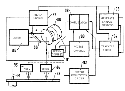
Figure 9 is a block diagram of a first embodiment of an
optical reader device in accordance with the invention.
The information medium 83 is carried by a rotary spindle
having an axis M and driven at a uniform speed of rotation, for
example. The reference surface of the information medium 83 is
illuminated by a laser source 85 via a semi-transparent blade 86,
a pivoting mirror and a focusing lens 84. The pivoting mirror
is ro~ated by a motor 88 so as to displace the light spot
formed by the lens 84 over the reference surface of the medium
83. This displacement takes place transversely relative to the
track element scan line. The light which has interacted with
the information medium is returned via the objective lens 84
and via the pivoting mirror and the blade 86 to photosensitive
means 87 which deliver an electrical read signal containing the
successively read information along each track element.
This electrical signal is applied to a sampling window
generator 93, to a circuit 94 for evaluating the offset of the
spot relative to the scan line and, if necessary, to a circuit
92 for identifying the special order permutation mark. A
control circuit 91 actuates the motor 88 as a function of two
input magnitudes which are the tracking error to be compensated
and the amplitude of the track sXip to be performed. The
~2fi3~,7~0
14
amplitude of the track skip is determined by a control circuit
90 which controls disk access depending on external read or
write requests and which is suitable for acting on an access
motor (not shown in Figure 9). The magnitude representative of
the tracking error is produced by the circuit 94 without taking
account of the permutation order of the prerecorded patterns
provided for the purpose. Consequently, the sign of the signal
delivered by the evaluator circuit 94 must be modified as
required, and to this end the invention provides for a commut-
ator circuit 84 to be inserted between the circuits 91 and 93in order to ensure that the tracking error signal has the
appropriate sign and thus ensure that the servocontrol loop for
compensating this error functions properly. The commutator
circuit 89 shown in Figure 9 comprises two stages connected in
cascade for swapping over the connections between its inlet and
outlet terminals as a function of two different commands. One
of these commands is provided by the circuit 90 when skipping
an odd number of tracks. The other command is providPd by the
circuit 92 for identifying the order permutation mark present
in one of the above-mentioned areas 78 and èncountered during a
scan.
If a track skip coincides with this mark being detected,
both stages change over thereby changing the sign of the error
twice over, and thus returning to the original sign.
In a variant, the information medium 83 may alternatively
be provided with a reference track which is solely constituted
by prerecorded marks relating to synchronizing its passage past
a read head. This applies, for example, if the information
medium is a disk including a ring which is concentrically
mounted with the annular area containing the track elements.
This ring may be indexed by a special mark concerning the
permutation order of the prerecorded marks situated in the
annular area where information is stored. The optical ring is
scanned by an auxiliary optical head 95 which delivers a read
signal characteristic of disk rotation. As illustrated ir.
dashed lines in Figure 9, this read signal takes the place of
the read signal from the detector circuit 87 as the input
~2~3~t
signal to the circuit 92. In this case, the zone 78 shown in
Figure 8 may contain a special signal indicative of sector
address scanning.
In Figure 9, the commutator circuit 89 is shown outside
the circuit 94 for determining the spot offset signal by
comparing the two read signal samples taken while scanning the
offset portions of the prerecorded patterns.
The samples may also be swapped over at the input to the
comparator circuit as shown in Figure 10.
The rectangle referenced 94 includes the circuit 89,
whereas the items outside the rectangle 94 are the same as in
Figure 9.
The circuit for evaluating the spot offset includes two
analog gates 96 and 97 which receive the read signal delivered
by the detector circuit 87. Each gate is controlled by a
sampling pulse from the generator circuit 93, but these two
pulses are applied to the gates 96 and 97 after being switched
by the circuit 89 in such a manner as to ensure that the sample
available at the output from the gate 96 is always
representative of interaction between the spot and a
prerecorded pattern whose offset is of predetermined sign. The
same situation applies to the other gate and to the other sign
of offset, so that the comparator circuit 98 always provides a
spot offset value of the appropriate sign~ This value may be
stored or smoothed by a circuit 99 prior to being applied to
the control circuit 91. The commutator circuit 89 is
controlled in the same way as before and it could equally well
have been integrated in tha generator 93.
The reader devices shown in Figures 9 and 10 may be
rendered compatible with reading information media using
prerecorded marks which are all arranged in the same order.
This can be done by locking the commutator 89 in a single,
preselected state. The circuit 92 for detecting the mark which
indicates that the order is being swapped over can readily
recognize which mode of operation to put into effect, if used
in conjunction with a timing circuit.
~263~
16
The invention is also applicable to prerecorded patterns
including two offsets of opposite sign. This version stems
from the configurations shown in Figures 6 and 7 where the
prerecorded patterns drift towards one another parallel to the
track element scan line until their centered ends meet. Since
the ends are lost by virtue of the X-shaped patterns meeting,
the ends of the centered patterns 50 may be used for defining
the transition code necessary for synchronizing the sca~. It
is also possible to add a centered pattern to the head or tail
end of the structure built up from meeting X-shaped patterns
such that the ~wo ends thereof provide the necessary additional
information for four-transition decoding.
If account is taken of the track element addresses read
from the medium, there is no need for special means to be
provided for indicating the order permutation. For example, if
two consecutive track elements have addresses numbered n and
n ~ 1, the change in parity may be used for selecting the
appropriate permutation. In this case, the circuit 92 in
Figures 9 and 10 is used to determine the parity of track
e~ement addresses and to indicate each parity change which
occurs during a revolution. The sector addresses could also be
used by detecting, for example, the changeover from the last
sector of one track element to the first sector of the next,
and by changing over the order permutation when the first
sector is encountered.