Note: Descriptions are shown in the official language in which they were submitted.
126376~
ELECTRON SPECTROMETER
This invention relates to an electron energy
spectrometer having an energy analyzer of the torroidal
capacitor type and which is adapted for analyzing
electrons emitted from the surface of a sample on
bombardment by a beam of primary radiation such as
X-rays, UV light or electrons.
Such spectrometers are used for the investigation of
sample surfaces because the energy of the emitted
electrons is characteristic of the chemical nature of
the bombarded surface. Consequently it is useful to
obtain information concerning the distribution of a
particular chemical species on the suface. A variety of
methods of producing an image of the surface utilizing
electrons having only a particular range of energies
are known. These include a projection method,
described by D.W. Turner, I.R. Plummer and H.Q. Porter
in Journal of Microscopy, 1984, vol.136 (2) pp 259-277,
in which secondary electrons travel along trajectories
determined by a powerful divergent magnetic field. The
electrons also pass through a retarding potential
energy analyzer so that images of the surface
comprising only electrons of certain energies can be
produced. An instrument of this type does not involve
any electrostatic lenses and requires a very large and
expensive magnet. It is quite different from the
spectrometers conventionally used for surfaca analysis
with which the present invention is concerned.
Another approach, described by C.T. Hovland at the
Third International Conference on Solid Surfaces,
Vienna, 1977 (pp 2363) is to recreate an image of the
2 126376~j
surface point by point by scanning a narrow beam of
primary radiation across the sample and analyzing the
secondary electrons with a conventional spectrometer,
eg a cylindrical mirror analyzer. Hovland suggests that
the sample is coated in a thin layer on an aluminium
substrate. A high-energy electron beam is then scanned
across the surface of the aluminium substrate so that
X-rays emitted at the point of contact of this beam and
the aluminium pass through the substrate and irradiate
a small area of the sample. This technique is limited
to use with samples which can be coated on an aluminium
substrate, which excludes a large proportion of the
samples usually investigated by X-ray photoelectron
spectrometry (XPS).
Electron microscopes having energy filters are well
known in the art and some are described by H. Watanabe
in J. Phys. Soc (Japan), 1962, vol. 17, pp 569, S.L.
Cundy, et al, J. Sci. Instr., 1966, vol. 43, pp 712,
D.B. Wittry, Brit. J. Appl. Phys, 1969, vol. 2 pp 1757,
A.V. Crewe et al, Rev. Sci. Instr. 1971, vol 42 (1) p
411, J.W. Andrew, et al, Proc. Ninth Int. Congress on
Electron Microscopy, Toronto, 1978, vol. 1 pp 40, and
R.F. Egerton, et al, J. Phys. E, 1975, vol 8 p 1033.
At first sight it would appear that an energy filtered
image of a surface which is emitting photoelectrons
could be produced by an electron microscope fitted with
such a filter, but in practice this is not possible.
All the instruments described operate with a very high
energy beam of electrons and the filters are used, for
example, for energy analysing electrons which have lost
energy by passing through the sample or for filtering
so that only electrons having energies within a narrow
band are used to form an image, thereby reducing the
chromatic defects of the microscope. Typically they
,~
~ 26376~
employ magnetic field energy filters such as that
described by Castaing, R and Henry, L in J.
Microscopie, 1964 vol. 3 (2) pp 13~, or electrostatic
lens filters such as that described by Mollenstedt and
Rang in Z.Angew. Phys, 1951 vol. 3 (5) pp 187. None
employs the torroidal or spherical sector capacitor
electrostatic analyzers conventionally used for the
analysis of low energy secondary, photo or Auger
electrons. Such instruments are therefore in fact
unsuitable for imaging surfaces emitting electrons at
low energies, as explained by Cazaux in
Ultramicroscopy, 1984, vol 12 pp 321-. Cazaux coated a
sample on a thin aluminium foil and produced the
incident X-rays according to the method of Hovland,
described above. The emitted electrons were passed
through the lens systems of an electron microscope
fitted with an energy filter of the type described by
Castaing and Henry in an attempt to form an energy
filtered image of the surface. However, Cazaux found
the results were unsatisfactory and that the images
obtained were in fact secondary electron images rather
than photoelectron images. He further showed that the
expected spatial resolution of the system would be low
when used with photoelectrons, and the expected
sensitivity would be so low as to make it very
difficult to produce an image of adequate contrast with
the small number of photoelectrons produced by XPS. In
general therefore, the extensive technology developed
for energy filtered microscopes is not applicable to
low energy electron spectrometers, and especially to
torroidal or spherical sector capacitor analyzers which
have not been used in this way with an electron
microscope.
It is well established in the field of surface analysis
that an electron energy analyzer based on a torroidal
lZ~3766
capacitor is the type best suited for the analysis of
low energy photoelectrons or Auger electrons. The term
"torroidal capacitor" is used herein to relate to
electrostatic energy analysers which comprise two
electrodes which are sectors of torroidal surfaces and
in which the equipotential surfaces are substantially
sectors of torroidal surfaces, at least close to the
electrodes. Most commonly the electrodes are sectors
of spherical surfaces (one of the range of possible
torroidal surfaces), often with a lBO sector angle,
but various angles between 90 and 270 are also
employed.
It is known that a properly designed analyzer of this
type possesses a pair of conjugate planes which are
such that a surface emitting monoenergetic electrons
situated in one plane will produce a two dimensional
image of that surface in the other plane. The energy
dispersion of the analyzer will cause this image to ba
dispersed according to electron energy along the energy
dispersion axis of the spectrometer in the image plane,
so that the spatial features of the image cannot be
distinguished from the energy spectrum at least along
this axis. N. Gurker, H. Ebel and M.F. Ebel, in Surface
and Interface Analysis, 1983, vol.5 (1) pp 13 -,
suggest that this can be overcome by imaging only a
narrow strip of the sample disposed so that the image
of the strip is perpendicular to the energy dispersion
axis in the image plane. Because the strip is narrow,
there is very little spatial detail along the energy
dispersion axis of the spectrometer and the energy
spectrum is independent of the image. A complete
two-dimensional image can be produced by mechanically
æcanning the sample so that different linear strips are
successively imaged by the spectrometer. An energy
spectrum may be recorded at each position of the sample
~ 5 1~6376~
relative to the slit using a two-dimensional position
sensitive detector situated in the image plane of the
analyzer. This information can be processed by computer
to yield complete two-dimensional images of the scanned
region of the surface and energy spectra corresponding
to each position of the sample. The chief disadvantage
of this method is the requirement to use a narrow slit
in the object plane of the spectrometer which clearly
prevents a large majority of the emitted photoelectrons
from reaching the detector. Consequently, the
sensitivity of the technique is low, and in view of the
relatively small number of electrons emitted in the
first place, this represents a serious proble~, as in
the case of the methods previously described. Greater
sensitivity is of course achieved by use of a wider
entrance slit, but this clearly reduces the resolution
of the energy spectrum and the spatial resolution along
one axis.
It is an object of the present invention, therefore to
provide an electron energy spectrometer with an
analyzer of the torroidal capacitor type which is
capable both of producing an energy spectrum of
electrons emitted from a small area of a sample and of
imaging at least a part of the surface of a sample
using electrons of a selected energy, and which does
not require the use of scanning techniques of any kind.
Such an analyzer is consequently more efficient than
previously known imaging analyzers, and overcomes the
problem of producing an energy filtered image with low
energy photoelectrons from XPS.
Viewed from one aspect the invention provides an
electron spectrometer operable to produce an image of
an electron emitting surface, said spectrometer
comprising in sequence:-
lZ6376fi
6 20208-1310
a) means for causing electrons to be emitted from
said surface;
b) a first lens system, for example a first electrostatic lens system,
arranged to project at least some of said electrons onto
a first diffraction plane as a Fourier transform
of an electron image of at least a part
of said surface;
c) a torroidal capacitor type electrostatic energy
analyzer having an object plane and conjugate
thereto a first image plane, said analyzer being
disposed with said object plane coincident with
said first diffraction plane and being arranged to
project electrons of said Fourier transform as an
energy dispersed Fourier transform in said first
image plane;
d) energy selection means for transmitting electrons
of said energy dispersed Fourier transform having
energies only within a selected range; and
e) a second lens system, for example a second electrostatic lens
system, arranged to receive electrons transmitted by aid energy
selection means and therewith to project an
electron image of at least a part of said surface
onto a second image plane.
In the case of an electrostatic energy analyser in
which the first image plane lies outside the
electrodes, the second electrostatic lens system (which
possesses a second diffraction plane) is disposed with
the second diffraction plane coincident with the first
image plane so that the final image is created in the
.~
7 126376~;
second image plane.
Preferably a transfer electrostatic lens system is
disposed between the surface and the first
electrostatic lens system and is arranged to receive
at least some of the electrons emitted from the surface
and to produce an electron image of at least a part of
the surface. If such a lens system is provided, the
electron image it produces serves as the object for the
first electrostatic lens system of the invention.
Preferably also, means disposed between the surface and
the analyzer are also provided for allowing into the
energy analyzer only those electrons which leave the
surface in directions which make a certain range of
angles to the surface. Further preferably, the
electrons leaving the surface are selected so that only
those which are travelling in directio~ which make a
certain range of angles to the axis of the first
electrostatic lens system ~or the transfer
electrostatic lens system, if provided) are allowed
into the energy analyzer.
In a further preferred embodiment, the electrodes
comprising the electrostatic energy analyzer are
sectors of spheres so that the analyzer comprises a
part-spherical electrostatic analyzer, for example of
the type conventionally used in electron spectrometers
operating at low pass energies. However, non-spherical
torroidal electrostatic analyzers may also be employed.
Preferably a first electron detecting means is provided
in or adjacent to the second image plane for either
visually displaying the electron image or for recording
it electrically. Such means are conventional and may
include a phosphor screen or a position sensitive
126376tS
detector, for example those described in US patent
4,395,636 or by M. Lampton and R.F. Malina in Rev. Sci.
Instruments, 1976, vol. 47 (11) p 1360. Other types of
position sensitive detectors may be used. Preferably at
least one channelplate electron multiplier is disposed
with its entrance in the second image plane in front of
the detector or the phosphor screen. However, where
further magnification (or reduction) of the image
produced by the second electrostatic lens system is
desired, an image magnifying electrostatic lens system
may be disposed between the second electrostatic lens
system and the first electron detecting means.
In a yet further preferred embodiment, the apparatus is
provided with means for adjusting the energy of
electrons passing into the energy analyzer. Thus the
potential of the central tra;ectory of the energy
analyzer and the potential of the surface may be
maintained at different values in order to accelerate
or retard the electrons to an energy particularly
suitable for analysis in the energy analyzer at a
desired resolution. Typically the sample is maintained
at ground potential, and the potential of the central
trajectory of the analyser and at least the entrance
and exit elements of the first and second electrostatic
lens systems, are maintained at a second potential
which can be adjusted to vary the degree of
acceleration or retardation as required. It is
particularly preferred that emitted electrons within
the energy band to be imaged in each imaging procedure
are accelerated or decelerated to the passband of the
energy analyzer. Preerably that passband will be
arranged about an energy of at least 50 eV,
conveniently 50 to 200 eV and specially about 100 eV.
The higher passband energy yields better spatial
resolution in the final image.
126376~;
In further preferred embodiments, either or both of the
transfer electrostatic lens system (if provided) and
the second electrostatic lens system are conveniently
of variable magnification.
As well as providing an electron image of at least part
of the sample surface, the invention offers the
possibility of recording the electron energy spectrum
of the electrons passing through the object plane of
the energy analyzer. An electron detector similar to
those described may be inserted into the path of the
electrons in the analyser image plane in order to
record the spectrum. As explained below, information
relating to the spatial features of the surface exists
in this plane in the form of the angles between
electron trajectories and the plane while the energies
are dispersed along the dispersion axis. Consequently a
spectrum recorded in this plane is substantially free
of interference from the spatial features of the
specimen. Typically, the spectrum detector is fitted on
a retractable mounting so that it can be withdrawn to
allow the electrons to form a real image of the surface
via the second electrostatic lens system.
Alternatively, if a spectrum detector containing an
aperture is used, the spectrum (except for the portion
falling on the aperture) and the image may be
simultaneously recorded. This is impossible on any
previously known electron energy spectrometer suitable
for analyzing Auger or photoelectrons. In such an
apparatus the means for detecting the spatial image
might if desired be omitted, and thus viewed from a
further aspect the invention provides an electron
spectrometer comprising elements (a) to (c) as defined
above and having an electron detecting means disposed
for the detection of electrons in said energy dispersed
126;~76fi
Fourier transform.
The first and second electrostatic lens systems of the
invention each may conveniently comprise one or more
electrostatic lenses, typically a simple conventional
three element cylinder lens.
If provided, the transfer electrostatic lens system
forms in the object plane of the first electrostatic
lens system an electron image of the sample surface.
Typically it comprises at l~ast two, and preferably
three electrostatic lenses, each of which is a
conventional three element lens. This allows the
magnification of the transfer lens system to be
selected independently of the position along the axis
of the image it produces. Such a system will desirably
be arranged to provide image magnification of a factor
of at least 16, preferably at least 25, and especially
at least 50, and a system capable of variable
magnification in the range x16 to x64 is particularly
preferred.
Advantage may also be gained by providing a similar
variable magnification system in the second
electrostatic lens system of the invention. The simple
three-element lens referred to above may then be
replaced by a multi-element two or three-lens system.
Preferably the electrostatic energy analyzer is of the
spherical sector type. Any suitable sector angle,
generally between 90 and 270 can be employed. Sector
angles of 190 or less, for example 150to 190, are
preferred for reasons of facility of component
mounting, but especially good results can be obtained
with a sector angle of about 180. The sectors of such
an analyzer typically do not physically extend to the
lZ6376'15
11
image and object planes, so that room is left for the
input and output slits which need to be positioned in
the image and object plan~s. Analyzers of this type are
known in the art and need not be described further.
Viewed from another aspect the invention provides a
method of forming an image of an electron emitting
surface, said method comprising:-
a) causing electrons to be emitted from a surface;
b) passing at least some of said electrons through afirst field, for example a first electrostatic field, arranged to
produce in a first diffraction plane a Fourier transform of an
electron image of at least a part of said surface;
:
c) passing at least some of the electrons of said
Fourier transform which travel through said first
diffraction plane through a second field which is an
electrostatic field generated by a torroidal capacitor type
electrostatic analyzer having an object plane
and a first image plane, said object plane being
coincident with said first diffraction plane,
thereby to produce an energy dispersed Fourier
transform in said first image plane;
d) selecting electrons which have energies within
a selected range; and
e) passing said selected electrons through a third
field, for example a third electrostatic field, arranged to focus
them to form in a second image plane a second electron image
comprising electrons having energies within said
selected range.
Preferably the electrons emitted from the surface are
12 1 26 3766
passed through a transfer electrostatic field before
the first electrostatic field. The transfer
electrostatic field is adapted to focus the electrons
to produce an image which serves as an obJect for the first
electrostatic field.
Preferably also the method of the invention
incorporates the step of selecting electrons which are
travelling in directions which make a certain range of
angles to the surface before they enter the first
electrostatic field.
In a further preferred embodiment, the method comprises
the step of changing the energy of the electrons before
they enter the second electrostatic field so that their
energies lie within a range in which the desired energy
resolution is obtained following energy dispersion by
the second electrostatic field.
,
In a yet further preferred embodiment, the
equipotential surfaces of the second electrostatic
field are part-spherical. Preferably also, the energy
of the electrons emitted from the surface is changed to
a value at which the energy analyzer will give the
desired energy resolution. This is a conventional mode
of operation of an electron spectrometer used for the
analysis of Auger or photoelectrons. See for example,
Brundle, Roberts, Latham and Yates, in J. Electron
Spectroscopy and ~elated Phenomena, 1974, Vol 3 pp
241-261. It will also be appreciated that a spectrum of
the energies of the electrons passing through the
second electrostatic field exists in its image plane
and can be recorded if required. This spectrum is such
that there is substantially no spatial information
contained in it. Further, the resolution of the image
formed in the second plane is substantially unaffected
13 1 Z6 376~
by the energy spread of the electrons which it
comprises.
In this way the problem of separating the energy
dispersion and the spatial imaging properties of a
torroidal capacitor electron energy analyzer can be
overcome. In a preferred embodiment, a sample is
bombarded with photons (X-rays, UV light, etc) to emit
photoelectrons, or with electrons to emit Auger
electrons, and some of the emitted electrons are
collected by the transfer lens system which produces an
image of the surface. As in a conventional analyzer,
the energy of the electrons may be varied by changing
the electrical potential of their environment, usually
to retard them so that the pass energy of the analyzer
can be set at a relatively low value, increasing the
energy resolution. In a conventional spectrometer,
such as that described by Gurker, Ebel and Ebel
(described previously), the transfer lens system causes
an image of the surface to be formed on the object
plane of the energy analyzer, which in turn forms an
energy dispersed image of the sample in its image plane
where a position sensitive detector is located. By
contrast, in the present invention the first lens
system is interposed between the image plane of the
transfer lens system and the object plane of the energy
analyzer. In the simplest case when the first lens
system comprises only a single thin lens, this will be
disposed so that the transfer lens system image plane
and the analyzer object plane are each situated at a
distance from the first lens system equal to the focal
length of the first lens system. Thus the object plane
of the analy~er coincides with a diffraction plane of
the first lens system in which a Fourier transform of
the surface image exists. Electrons leaving a
particular point on the sample surface in directions
14 1;2~376~
which make a certain range of angles to the surface
will pass through the diffraction plane of the first
lens system in the form of a substantially parallel
beam inclined at a specific angle to the plane, while
electrons leaving a different point on the surface pass
through the plane at a different angle. Thus there is
substantially no intensity variation in the plane due
to the spatial features of the surface. The torroidal
capacitor energy analyzer forms an "image" of this
diffraction plane in its imag~ plane and also
introduces energy dispersion of the electrons along one
axis (its dispersion axis). Thus electrons from
different points on the sample pass through the image
plane of the analyzer at different angles, but are
displaced along the dispersion axis according to their
energy. Consequently the intensity varies along this
axis according to the energy of the electrons, while it
is largely independent of the point on the sample from
which the electrons originated (assuming a uniform
sample surface). This allows a complete energy
spectrum, substantially independent of the spatial
features of the surface, to be recorded in the image
plane of the analyzer.
If, however, the electrons passing through the image
plane of the analyzer are received by a second lens
system suitably situated then another image of the
surface will be formed by that lens, i.e, the second
lens system reverses the effect of the first lens
system. In the case where the second lens system is a
single thin lens, this will be disposed so that the
image plane of the analyser is spaced from the lens by
a distance equal to its focal length, and the image
will be produced in the image plane of the lens, also
spaced from the lens by a distance equal to its focal length.
This image is independent of the energy dispersion of
15 ~ 26 3766
the electron distribution in the analyzer
image plane because it comprises a
Fourier transform of the analyzer image plane and is
consequently dependent only on the angles at which the
electrons pass through that plane. The energy band of
the electrons comprising this image can of course be
selected by varying the pass energy of the analyzer,
the difference in potential between the sample and the
central trajectory of the analyzer (i.e. the retarding
ratio), and/or the width of a slit situated in its
image pl an~3 .
It is also desirable to limit the angular range of
electron trajectories entering the analyzer by means of
another slit disposed in the object plane of the
analyzer.
It is therefore possible to select electrons
characteristic of a particular element in the surface
and produce an image of the distribution of that
element over the surface. Alternatively, the energy
spectrum of electrons from a particular region of the
surface can be recorded. A suitably shaped aperture
disposed in the transfer lens system in a plane where
an image of the surface is formed can be used to select
the region of the sample to be imaged by the
spectrometer. It will also be seen that by using a
detector in the analyzer image plane which contains an
aperture to allow some electrons to enter the third
lens, a large part of the spectrum can be recorded
simultaneously with the production of an image of the
surface. Alternatively, a detector may be used which
contains an aperture or slit which extends only part
way along the axis in the image plane of the analyzer
substantially perpendicular to the dispersion axis. In
this way a complete energy spectrum can be recorded in
16 1Z6376~5
one part of the image plane while an image of the
surface can be created from the electrons which pass
into the final lens through the aperture in the
detector.
This process is clearly more efficient than a scanning
process and uses the maximum possible number of the
electrons emitted by the surface.
A preferred embodiment of the invention will now be
described in greater detail by reference to the
following figures in which:-
figure 1 is a schematic drawing of an embodiment ofthe spectrometer of the invention showing the
positions of the various lens elements and images;
figure 2 is a diagram of the ob~ect and image
planes of an electron energy analyzer suitable for
use in the spectrometer of the invention,
illustrating some of the parameters raferred to
below;
figure 3 is a schematic drawing of a transfer lens
system and first electrostatic lens system suitable
for use with the invention;
figure 4 is a drawing of the major components of a
spectrometer according to the invention;
figure 5 is a drawing illustrating a practical
embodiment of the transfer lens system and first
electrostatic lens system shown in figure 3; and
figure 6 is a drawing illustrating an output lens
and detector suitable for use with the invention.
1.26376~i
17
Referring first to figure 1, electrons emitted by an
object 4 are focused by a transfer lens system
described in detail below, which comprises
electrostatic lenses l and 2. The transfer lens system
produces a real image 3 of the object 4. Image 3 is
located a distance F2 from a first electrostatic lens
system 5, which in turn is located at F2 from the
object plane 6 of a hemispherical capacitor electron
energy analyzer, the central trajectory of which is
shown at 7. Object 4, and the transfer lens system
entranc~ and exit elements (15 and 25, figure 5) are
maintained at ground potential while the potential of
central trajectory 7 and the entrance and exit elements
of lens system 5 (27 and 32, figure 5) is adjusted to
obtain the desired retardation (or acceleration) of the
electrons before they enter the energy analyzer. In the
case when lens system 5 is a single thin lens, distance
F2 is made equal to the focal length of lens system 5,
so that a Fourier transform of image 3 exists in ob;ect
plane 6. Electrons passing through plane 6 pass into
the energy analyzer, and those having energies within
the range passed by the analyzer pass through the
analyzer image plane 8 which is conjugate to plane 6.
An aperture disposed in plane 8 allows the passage of
electrons with a selected range of energies, as in a
conventional electron energy spectrometer. The Fourier
transform of image 3 which exists in plane 6 is
therefore reproduced in plane 8, but with energy
dispersion of the electrons comprising it along an axis
lying in plane 8, as explained. A second electrostatic
lens system 9, disposed at a distance F3 from plane 8
(where F3 is the focal length of lens system 9,
assuming that lens system 9 is a single thin lens),
causes a second electron image 10 of object 4 to be
formed at a distance F3 from lens system 9 fro~ the
- - .;.,~ , , ,
18 126376~S
electrons passing through the aperture in plane 8. In
other words, lens system 9 operates to convert
electrons having energies within the selected range
from the energy dispersed Fourier transform existing in
plane 8 into the image lO which is recorded in a
conventional way using a position sensitive detector.
As explained, image lO is not affected by the energy
dispersion which exists in plane 8.
Referring next to figure 2, R is the radius of the
central trajectory 7 of a part-spherical energy
analyzer havlng its entrance face 11 and exit face 12
both inclined at an angle ~ to the object plane 6 and
image plane 8, respectively. Also shown in figure 2,
r(0) is the polar coordinate of the trajectory 13 of an
electron which has travelled an angle 0 through the
analyzer from entrance face 11.
It can be shown that the position of the electron on
trajectory 13 is given by equation [1]:-
r(0)- = 1 + 6(1 - COS0) + ~(tan~cos0 + sin0) + pcos0
+ 62(COS 0 - COS0)
~ ~x2(-tan2~sin20+cos0 - cos20+2tan~sin0cos0)
+ ~p(-2tan~sin20 + 2sin0cos0)
+ p2 ( - sin20 )
+ ~6 ( 2sin0 - 2sin0cos0 + 2tan~sin20)
+ 6p (2sin20) + etc -[1]
In equation [1], p is the normalised height of an
object situated in the object plane 6 of the analyzer,
(i.e. the actual height = Rp), ~ is the angle between
the normal to face 11 and the direction at which
electrons which will travel through the analyser on
9 1263765
trajectory 13 approach face 11, and 6.E is the
difference in energy between the electrons travelling
along trajectory 13 and the pass energy E of the
analyzer.
At the exit face 12 of the analyzer, 0 = 180 - 2~, so
that from equation [1],
r (0)
2 = 1+~(1 + cos2~)+~(-tan~cos2~+sin2~)+p(-cos2~)
+ ~2(CoS22~ + Cos2~)
~ ~X2( -tan2~Sin22~-coS2~-coS22~-2tan~sin2~cos2~ )
+ ~p(-2tan~sin22~ - 2sin2~cos2~)
~ p2( -sin22~ )
(2sin2~+2sin2~cos2~ + 2tan~sin22~)
+p(2sin22~) + etc. -[2]
..
At the exit face 12 of the analyzer, the gradient of
the tra~ectory 13, l.dr , is g$ven by equation [3]:-
r d0
tan~2 = l [drl ~[3]
0=02
In equation [3], ~2 iS the angle at exit face 12
between the trajectory 13 and the normal to face 12,
(on the electron approach side of face 12), and r2 is
the value of r at 0 = ~2, where 02 iS the value of 0 at
face 12.
From equations [1]-[3], the following expressions can
be derived:-
"", . . .
. 20 ~2~37~
a2 ~ = 6 ( 2sin~cos~) - a + p( -2sin~cos~)
+ 62(-2sin~cos~) + a2(-2Sin~COS~)
+ ~a(4sin2~) + ~p(4sin~cos~)
+ etc. ~[4]
where a2 ~ iS the angle at exit face 12 between the
trajectory 13 and the normal to face 12, on the
electron exit side of face 12
and p ~ 2 6 - p
+ 3( 2-4Sin2~ + 4Sil14~ )
+ a2( -2-2tan2~Sin2~ + 2tan2~Sill4~ + 4sill4~ )
+ P (-4sin2~ + 4sin4~)
+ ap( -4sin~cos~
+ a6 ( 8sin~cos~ + 4tan~sin2~)
+ 6p( 12sin2~ - 8sin4~)
+ etc. ~[53
in which P2 is the normalized displacement of the
electron trajectory 13 from the central trajectory 7 on
image plane 8 (i.e., the actual displacement = Rp2).
It is clear from equations [4] and [5] that it is
preferable to utilize an energy analyzer in which ~=0,
that is, a 180 sector analyzer, because when ~=0, the
second order terms in the equations become zero and the
aberrations of the analyzer are consequently minimized.
However, it is within the scope of the invention to
21 ~26376fi
utilize an analyzer in which ~0. The procedure for
selecting the optimum embodiment for such an instrument
will be similar to the following example which is given
for a 180 analyzer, but equations [4] and [5] must be
substituted for equations [6] and [7], and the most
important aberrations minimized by an appropriate
design.
In the case of a 180 sector analyzer, ~=0 and equations
[4] and [5] respectively become:
~21 = -~ ( + 3rd. order terms) -[6]
and P2 = ~6 - p + 262 _ 2~2
+ ( 3rd. order terms) -[7]
Assuming that the coefficients of the third order terms
are approximately unity, it follows from equations [6]
and [7] that the angular error a~2' (which gives rise
to a blurring of the image after the electrons have
passed through lens 9) will not be greater than about
10 4 when ~, ~, and p do not exceed approximately 0.05,
which is easily achieved in practice. Therefore, if the
focal length of lens 9 (F3, figure 1) is 150 mm, the
displacement error F3a~2' in the final image 10 will be
approximately 15 micron, that is, about the same as the
resolution of a conventional position sensitive
electron detector. Thus the focal length of lenses 5
and 9 may conveniently be 150 mm, making the
aberrations of the analyzer approximately equal to the
resolution of the detector.
If, however, a 150 sector analyzer is used, ~=15 and
the spatial resolution F3a~2'(when ~, 6 and p do not
exceed 0.05) is of the order of several mm when F3 =
150 mm, which clearly illustrates the advantage of
using a 180 sector analyzer.
, 22 12fi3766
As explained, the potentials applied to lens system 5
and to the analyzer electrodes may also be arranged to
change the energy of the electrons emitted from the
sample to the desired pass energy of the analyzer. This
should be done without significantly degrading either
the spatial or the energy resolution of the analyzer. A
practical design may be arrived at in the following
way.
One way of ensuring that the magnification of the
system is independent of the analyzer pass energy is to
make the retardation plane coincide with a spatial
image. Further, after retardation, the angular
divergence of the beam becomes much greater, and the
chromatic aberrations of the various lenses are likely
to become the most important factors controlling the
overall spatial resolution.
Considering the system of lenses illustrated in figure
3, plane 14 represents the retardation plane of the
lens system which is coincident with image 3. To the
left of plane 14, electrons have energy Eo while to
the right they have energy E , the pass energy of the
analyzer.
The contribution to the chromatic aberration at the
object 4 from lens system 5 is given by equation [8]:-
1 E 3~2 dE
~c M2 E C (5) . ~O . - -[8]
where ~ is the contribution to the chromatic
aberration due to lens 5 at object 4,
is the angular divergence of the electron beam
23 126376~
at object 4,
C (5) is the chromatic aberration coefficient of
lens 5,
M is the magnification of image 3 with respect
to object 4 by lenses 1 and 2, and
dE is the energy passband of the analyzer.
In order to ensure that the effect of the chromatic
aberration due to lens 5 is acceptably small, the
magnification M of lenses 1 and 2 must be made large
enough to overcome the amplification (Eo/E ~3/2 of the
chromatic aberration coefficient of lens system 5.
Typical operating conditions might be Eo = 885 eV and
~ = 12.5 eV, so that M = 24.4 when (Eo/E )3/2/M2 = 1.
Therefore, if the chromatic aberration of lens 5 is to
be insignificant in comparison with that of the
objective lens system, M ~ 24. This implies that the
retardation should preferably take place at image 3
rather than at any previous image where the
magnification would be smaller, and the contribution of
the chromatic aberration from lenses between the retard
plane and lens system 5 would be correspondingly
larger.
Considering next the effect of spherical aberration of
the lenses on the spatial resolution of the system, the
contribution ~ to the resolution from spherical
aberration is given by equation [9]:-
= ~C ~0 -[9]
9 g
where C is the spherical aberration coefficient of the
, ...... .
24 ~2~376fi
entire lens system, which will be dominated by the
spherical aberration of the objective lens system 1.
The contribution ~ to the resolution from the
chromatic aberration is given by equation [10]:-
~ = CC~o.dE/Eo -llO]
where C is the chromatic aberration coefficient of the
entire lens system.
As explained previously, providing that M is
sufficiently high, only lens system 5 and lens system 1
will contribute significantly to the total aberrations.
Therefore,
(Eo/E )3/2
CC = CC~1) + CC(5) ' M2 -[11]
where C (1) is the chromatic aberration of lens system 1.
ChoSing ~8 = ~c ' - [ 12]
and from equations [9] and [10],
/3
dE = s o ~2/3 -[13]
l 4 Cc
and from equation [93,
1/3
4~
~o = _ -[14]
C
In the case where the width of electron beam at object
plane 6 (di ) is small, then dE can be controlled by
selection of the exit slit width (d ), so that
~fi~7~;
out ( 2R.dE/EC) din -[15]
Further, from the Lagrange-Helmholtz relationship,
2F ~ E 1/2
d = 2 0 E -[16]
c
so that from [15],
dE 2F ~ r E l
d = 2R.- _ 2 L ~ -[17]
Alternatively, in the case where di is greater than the
desired value of d t~ then ~0 and dE must be adjusted
so that the input beam width is equal to d t ~ SO that
d = d = R(dE/E )
in out c
and 8 = ~ while s < c -[18]
From equations [12],[16] and [18],
MR dE
~ 2F E l/2E 1/2 -[19]
2 c O
and
dE = [ - ~ E / Eo /4~1/2 -[20]
In equations [9] - [20], ~ represents the blurring of
the final image referred to object 4, that is, the
smallest element which can be resolved by the system.
The count rate X' from an image area ~ into a cone of
semi-angle ~ is given by equation [21]:
12~376fi
26
X' = ~'(Eo)dE.~.~o2~2 -[21]
where ~'(Eo)dE is the brightness of the electrons
emitted from the object 4 in the energy band Eo to
(Eo + dE). From equations [10], [12], and [21],
X' = Eo ~4 -[22]
Cc dE
Equation 22 shows that in order to maximise X' for a
given resolution ~, C and dE must both be minimized.
From equation [11] it can be seen that if M is very
large, the minimum value of C is C (1), and because it
is always possible to reduce di so that equation [13]
rather than equation [20] is operative, the maximum
value of X' (X'(max)) will be given by equation [23]:-
_ 1 l/3 _ ~10 3
X'(max) = ~ (Eo)-~ C ~ C (1) -[23]
Values of dE, doUt, ~0 and X'can be calculated for any
proposed arrangement of lenses from equations [13],
[17], [14] and [22] in the case when di < d t or from
equations [20], [18], [19] and [22] when di = d
Table 1 lists some typical values for chosen values of
~ Ec and M.
~26376fi
27
TABLE 1
_ ¦ Ec(eV)ll 12.5 ¦¦ 50 ¦¦ 100
__ _ __
~ M 16 64 16 64 16 64
(~m) Cc(mm) 1440 399 469 339 379 333
__ _ _
dE 2.5 0.14 0.25 0.35 0.29 0.47 0.30
(eV)10 0.28 0.62 0.70 0.73 0.93 0.75
0.56 1.57 1.41 1.85 1.86 1.88
2.5 1.71 5.11 1.06 1.30 0.70 0.59
(mm)10 3.41 13.5 2.11 3.68 1.40 1.75
A0 6.82 35.5 4.23 9.99 2.80 4.85
2.5 11 22 15 22 1322
o10 22 36 27 36 2536
(mrad)
, . 40 43 57 54 57 5057
: X'(max) _
` X' 2.5 0.08 0.01 0.07 0.03 0.08 0.04 0.08
:~ (cps)10 8.4 1.19 6.99 4.47 ~.21 5.16 8.28
854 152 706 569 830 660 846
The underlined values in Table 1 are those for which
d = d
in out
The values of C and C required in the equations can
be found from the tables for electrostatic lenses given
by E. Harting and F.M. Read in "Electrostatic Lenses",
Elsevier, 1976. Note that C is assumed to be due
almost entirely to lens system 1 (equation [9]),
and in practice the first element of lens system 1,
while C is determined by lens system 1 and also lens
5 (equation [ll]). In Table 1, the following dimensions
have been used:-
~ 263'76~
28
lens 5:- focal length (F3) = 150mm
diameter = 60mm
lens 1:- focal length = 64mm
diameter = 32mm
Other parameters used to determine C and C , using the
terminology of Harting and Read, are A/D=l, G/D=0.1,
D1=D2, and V1=V3, which are typical for conventional
three element lenses.
The contribution of lens 9 to the overall aberrations
can be estimated from equations t24] and [25], which
give the spherical (~ (9)) and chromatic (~ (9))
aberrations due to lens 9, referred back to the plane
of object 4. The semi-angle of a cone of electrons
converging on a point in the image 10 after
transversing lens system 9 is doUt/2F3, where F3 is the
focal length of lens 9, so that if lenses 5 and 9 are
identical (i.e., the magnification of image 10 relative
to object 4 is equal to the magnification of image 3
relative to object 4),
[ 3 ~ [ ~ - [ 24]
and
[ 3~ [ ~ M ~
in which C (9) and C (9) are respectively the spherical
~ 2637~fi
29
and chromatic aberration coefficients of lens 9, which
can be found from the tables given by Harting and Read.
Using equations t24] and [25] it can be shown that
A ( 9 ) and ~ (9) are insignificant in comparison with a
chosen value of ~ providing that M is approximately 25
or greater, and E is 50 eV, or greater.
Table 1 also shows that the highest values of X' are
obtained by using the highest values of E (50 and 100
eV). Also, ~ (9) and a (9) are less than 1% and 20% of
~ respectively when using the highest values of E ( 50
and 100 eV) when M is either 16 or 64. Consequently a
preferred embodiment utilizes a pass energy of between
50 and 100 eV and a variable magnification of between
16 and 64, selected to suit the fineness of detail and
the field of view required. Optimum values of ~ and
d t for a given resolution will vary slightly with M,
but this is not a serious problem. In general there is
a unique combination of ~0 and doUt for given values of
M, E and E which yields the maximum count rate at a
given resolution ~, and these values can be predicted
for the preferred embodiment from the equations given.
Following the procedure outlined, similar sets of
equations can be derived for any particular type of
analyzer and lens system, and the parameters optimised
for maximum performance.
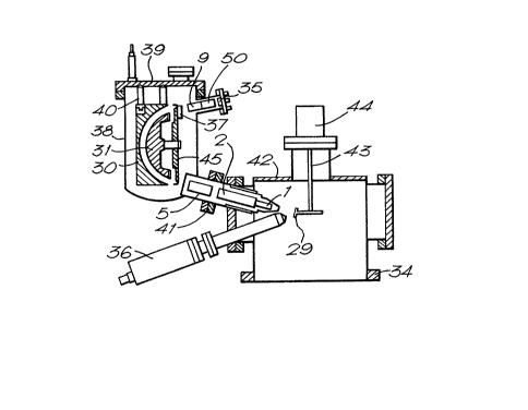
The disposition of the major components of the
invention is shown in figure 4. The energy analyzer
comprises an outer hemispherical electrode 30 supported
on insulators 40 from a lid 39 of analyzer vacuum
housing 38. Inner hemispherical electrode 31 is
supported from electrode 30 by other insulated supports
(not shown). Housing 38 is connected by means of
flange 41 to sample chamber 42 which in turn is
126376fi
connected by flange 34 to a vacuum pump, typically a
diffusion pump (not shown). Sample 29 is supported with
the surface to be examined disposed in the plane of
object 4 (figure 1) by means of rod 43 from a
manipulator 44. The energy analyzer entrance and exit
apertures are mounted on one or more rotatable plates
45 so that different pairs of slits can be brought into
use by rotating the plates. An electron detector 37,
preferably a position sensitive detector, is
conveniently mounted on one of rotatable plates 45 to
enable the energy spectrum to be recorded when
required. Detector 37 may also contain an aperture to
permit simultaneous recording of the energy spectrum
using detector 37 and a spatial ~ge using detector 35
(discussed below).
A primary beam generator 36 is also fitted to chamber
42, and irradiates sample 29 with a beam of particles
or radiation which cause emission of secondary,
photoelectrons or Auger electrons from the sample.
Generator 36 is typically an X-ray, electron, ion beam
or U.V. llght source. In common with all surface
investigation apparatus of this type, the pressure in
chamber 42 and housing 38 is maintained at 10-8 torr or
lower.
The various electrostatic lens systems are disposed
adjacent to the entrance and exit apertures of the
analyzer, as shown in figure 4. A position sensitive
detector 35 is used to record the image of the sample
which is formed in the image plane of lens 9. Detector
35 preferably comprises a wedge and strip detector, as
explained. Electronic signal processing equipment for
generating a visual or printed image from such a
detector is well known in the art.
31 1.2~376fi
In the case where a magnified image of the image
produced by lens system 9 is required on detector 35,
the second electrostatic lens system of the invention
may comprise both lens system 9 and an auxillary lens
system 50 (figure 4) which is preferably a zoom lens
with variable magnification. Lens 50 may then be used
to match the resolution of the final image produced by
the second electrostatic lens system to the resolution
of detector 35.
The power supplies required to maintain the various
electrodes of the spectrometer system at the required
potentials are also well known in the art.
If an apertured detector 37 is used to detect an energy
spectrum simultaneously with the detection of the
spatial image using detector 35 then a gap will exist
in the recorded spectrum caused by the aperture in
detector 37. Providing that this gap is not large
compared with the fine detail of the adjacent parts of
the energy spectrum, tha missing spectrum can be
interpolated using the integrated count rate from
detector 35.
Figure 5 illustrates a practical embodiment of the
transfer lens system and first electrostatic lens
system of the invention. An objective lens comprises
the three elements 15, 16 and 17 which are maintained
at potentials V , Vl and V , respectively. The
objective lens is adapted to form an image of the
surface of sample 29 in the plane of aperture plate 20.
The aperture in plate 20 is preferably adjustable in
size in order to select the portion of the surface to
be imaged. A second adjustable aperture plate 18, is
disposed as shown in the focal plane immediately
following the objective lens, which is situated at a
~2~376~S
32
distance approximately equal to the focal length of the
objective lens from the centre of element 16. The
aperture in plate 18 is used to control the angle ~ .
Transfer tube 19 is provided to ensure that the paths
of the electrons are not affected by stray
electrostatic fields. Sample 29, aperture plates 18 and
20, and tube 19 are maintained at potential V , usually
earth, while V1 is adjusted to cause an image to be
formed in the plane of aperture plate 20. A stigmator,
comprising eight electrodes 26 disposed symmetrically
at one end of transfer tube 19, is also provided to
enable the astigmatism introduced by the lens system to
be corrected.
Lens elements 21, 22, 23, 24 and 25 comprise a pair of
electrostatic lenses which form an image in the
retardation plane 14 from the image formed at aperture
plate 20 by lens system 1. Potentials V2 and V3,
applied to elements 22 and 24 respectively, are
adjusted to sst the magnification of the lens system to
the desired value. Elements 21, 13 and 25 are
maintained at potential V . Elements 21, 22 and 23
(left hand part) are conveniently 20mm diameter and
elements 23 (right hand part~, 24 and 25 may be 60mm
diameter.
Elements 27, 28 and 32 comprise lens system 5 (figure
1), and are maintained at potentials V5, V4 and Vs
respectively. The aperture in aperture plate 33
comprises the entrance aperture of the energy analyzer
which is disposed in plane 6 (figures 2 and 3).
Electrons passing through the retardation plane 14,
which lies between lens elements 25 and 27, are
retarded (or accelerated, if Vs is more positive than
V ) as they pass from potential V to potential Vs and
the electrons which will form the detected spatial
; 33 ~ 26 376~
image emerge with energy E (the pass energy of the
analyzer). The function of lens system 5 has been
described earlier.
Figure 6 illustrates a suitable practical arrangement
for the second electrostatic lens system 9.
Elements 47, 48 and 49, maintained at potentials V5, V6
and V5 respectively, comprise a three element lens
which forms an image on position sensitive detector 35
in the manner described. Aperture plate 46, disposed in
plane 8, provides the exit aperture of the energy
analyzer. The potential V7 of the detector 35 is
maintained several hundred volts more positive than Vs
in order that electrons leaving the lens are
accelerated and impact the detector with sufficient
energy to ensure efficient operation of the detector.
It will be understood that the lens systems shown in
figures 5 and 6 is intended only as an example, and
that other arrangements may be used.