Note: Descriptions are shown in the official language in which they were submitted.
63~
ANDOOl
--2--
Background of the Invention
The present invention relates to the formation of a
coating having a cermet structure and devices usable
therewith, preferred uses being for optical data
recording.
: It is known that data can be recorded by selec-
tively illuminating a material so a~ to selectively
change a reflectance of specific portions of the
material, such iLlumination being done using high
powered lasers. To read the data, the material is later
illuminated with a low powered laser, and differences
in reflection from various bits of the material are
detected as either a "11' or a "O".
Materials used for this purpose suffer several
drawbacks~ since oftentimes relatively high power den-
sities are required to adequately change a reflectance
of~a portlon of the material so as to obtain a desired
,
~ AND001
signal-to-noise ratio upon reading~ In addition, such
materials are oftentimes environmentally unstable~ and
therefore require the use of additional protective
layers thereover. Furthermore, such materials have also
proved difficult to make in a controlled fashion, and
hence are relatively expensive.
An example of a prior art optical recording
material or sub-trate is described by Chao "New Media
Development at Burroughs: Material and Coating",
Optical Data Storage, SPIE Vol. 382, pages 14~-156.
According to this reference, a tri-layer structure is
formed which is composed of a reflective mirror layer
; over which is disposed a quarter wave length dielectric
spacer layer over which is disposed a very thin metal
absorber layer over which is disposed a thick overcoat
protective layer. A preferred example for the metal
absorber layer is gold. The gold is deposited in such a
way so as to control its thin film microstructure ~uch
that the microstructure can be altered by laser heating
to ~orm an aggregated discontinuous structure whose
: :
::
~i3~l~
AND001
--4--
reflectivity changes subsequent to being heated.
Jipson, "The Writing Mechanism for Discontinuous Metal
Films", Optical Storage Media, SPIE Vol. 420, pages
344-48, describes a mechanism by which a reflectivity
of a metal absorber layer disposed on a PMM~ substrate
is changed by laser heating.
Substrates and coatings of the type described and
analyzed by these two references are disadvantageous
since optical, chemical, and mechanical properties ot
the metal coating layer are difElcult to control during
manufacture. Specifically, though the thickness of the
metal layer can be varied to vary its absorption,
reflection, and transmission, these variables cannot be
independently controlled for any given metal to obtain
optimum writing recording thresholds or optimum signal-
to-noise ratios upon reading. In addition, since metals
are excellent heat conductors, metal coatings are
disadvantageous since relatively high writing powers
are required to locally change the reflectance of the
metal coating due to the metal's tendency to rapidly
disperse heat over a wide area.
: :
~2~
AND001
--5--
Summary_of the Invention
Accordingly~ it is an object oE the present inven-
tion to provide an optical recording coating and device
therewith which does not have the above-noted
drawbacks, which has a relatively low recording
threshold, which can be made to be environmentally
stable, and which can be tailored so as to have desired
optical, mechanical, and chemical characteristics.
These and other objects are achieved by a coating
comprising a cermet which includes a layer of metal
particles dispersed in a solid dielectric matrix, pre-
ferably a ceramic, the metal particles and dielectric
matrlx being co-deposlted on a substrate, preferably
made of a polymer, the coating being formulated such
that upon being illuminated by high powered light a
localized optical reflectance of the coating changes so
as to be capable of recording data therein. In par-
ticular, the mètal particles of the cermet are selected
: ~ ~ : ; :
~: ; `
~: ~
;:
~3~
AND001
--6--
from a group of metals having relatively high mel-ting
points, these metals for example being nickel, copper,
rhodium, palladium, silver, platinum, and gold. In
addition, the dielectric or ceramic material is one
which also has a xelatively high melting point, pre-
ferred examples including oxygen being SiO2, SnO2,
In23~ GeO2, Ti2, Ta205, ZnO, ZrO~, Y203, and CdO,
and examples of dielectric materials including nitro-
gen being Si3N4, TiN, and other tran3ition metal nitri-
des. Accordingly, the invention comprises ~orming the
cermet using metal particles which khemselves have a
relatively high mel.ting point and dispersing them in a
ceramic matrix ~orm such that the ceramic matrix also
has a relatively high melting point. A particularly
preferred embodiment of the invention is a cermet
comprising gold particles disposed in a silicon
dioxide ceramic matrix.
one preferred method of forming the optical coating
of the invention is by sputtering, and preferably reac-
tive sputtering, whereby a sputtering target comprises
.
~ ~63~
ANDOOl
--7-
a metal to be deposited, with a sputtering cham~er
including the target having therein an ionizable inert
gas, such as argon, and other gases capable of forming
a dielectric matrix of the cermet during -the sputtering
process. By applying a high voltage diEferentiaL bet-
ween an anode and the target~ which comprises a
cathode, the target is co-deposited on the substrate
with the dielectric matrix, with densities of the gases
constituting the dielectric matrix being carefully
controlled during the sputtering process so as to vary
and optimize the properties of the coating so formed.
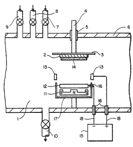
Brief Description of the Drawin~
Figure 1 is a partial cross-sectional view of a
sputtering apparatus for forming coatings in accordance
with the invention.
:; :
ANDOO1
--8--
Description of the re~erred Embodiments
According to the invention, a novel optical
recording device includes a cermet structure layer 14
disposed on a surEace of a polymer 2, with the layer 14
being constructed and dimensions such that its reflec-
tance from a source to a detector~ both relatively
fixed in space, substantially and permanently changes
subsequent to illuminating the layer 14 with high power
light, such as can be supplied from a high powered
laser, preferred embodiments including the use of a
semiconducting laser. The change in re~lectance can be
used to denote either an on or an off state, e.g. a "1'
or a 1-0ll, with little or no change in reflectance
denotlng the converse. Hence, to write information on
such a device, successive portions of the layer are
illuminated with a high powered laser appropriately
modulated such that selective bits of the layer undergo
a change in reflectance. To read the information, the
device is later illuminated with a low powered laser,
and reflection intensities from successive bits of the
:~
~Çi3~
AND001
_9_
layer are detected, with a high reflectance denoting
either the 1 or the l and a low reflectance indicating
either the 0 or the 1.
Various metals can be chosen for the target 12,
with preferred metals being those with high melting
points such metals including, but not being limited to,
gold, nickel, copper, platinum, palladium, and rhodium.
Also, various dielectric materials can be formed, with
pre~erred dielectrics being those with high melting
points as well t examples oE such dieLectric materials
including oxygen being SiO2, SnO2, In203, GeO2, TiO2,
Ta20s, ZnO, ZrO2, Y203~ and CdO, and examples of such
dielectr~c materials including nitrogen being Si3N4,
TiN, and other transition metal nitrides.
:
A particularly preferred embodiment is a ¢ermet
consisting essentially of gold particles dispersed
throughout a silicon dioxide ceramic matrix this embo-
diment being advantageous since gold is an extremely
: stable metal and silicon dloxide is also an extremely
~2639~ ANDOO1
--10--
stable material, thus resulting in an optical recording
coating which i9 highly stable in nature and hence long
lasting.
The change in reflectance induced by the high
powered laser is believed to b~ the result of layer 14
changing in structure due to the heat absorbed therein
which seems to result in the metal particles at least
partially agglomerating. It is desirable that the
substrate be made of a material which does not unduly
retard or inhibit the desired agglomeration of the
metal particles.
Substrates to which the layer is applied pre-
ferably have a smooth surface, and in general prefor-
mating structure on the substrate is included to help
identify where the data is contained, the preformating
structure being non-uniform and being much larger in
slze than a laser spot diameter used in writing or
reading. Also, the surface of the substrate exclusive
of the preformating structure can be non-uniform by
~2~
AND001
using a fine textured structure, wherein "bumps"
defined by the textured structure are significan~ly
smaller than the laser spot diameter.
Since during reading an optical detector essen-
tially remains fixed in space relative to an optical
source (the low powered laser) and the layer 14, a
change in the direction of the re~lectance of the layer
14 is interpreted as a decrease in reflection. Metal
particle agglomeration and substrate deformation are
both capable of changing a direction of the reflectance
of the layer 14. Since deformation of the substrate is
a desirable phPnomenon during writing it is pre~erable
to dispose the layer 14 on a substrate having a rela-
tive low heat distortion point of approximately 130UC,
possibly as high as lS0UC, 200~C, or 220~C, since such
relatively low heat distortion points of the substrate
result in the substrate possibly being locally altered
or deformed when the layer 14 is illuminated with a
high light power density. Accordingly, preferred
substrates of the inventlon lnclude polymers, preferred
.
:;
~:
~2G~
-12- ANDOOl
embodiments comprising polycarbonate, acryl.ates, ~e.g.
PMMA), and polyester, though other high melting point
substrates are possible where the substrate does not
unduly retard or inhibit agglomeration o~ t:he metal
particles.
Coatings o~ the invention can be uniquely formed
to provide a wide variety of desired optical, chemical,
or mechanical properties by forming the coating on the
substrate by reactive sputtering, one example of which
will be described by reference to Figure 1.
Figure 1 illustrates a sputtering chamber 1 having
a substrate 2 onto which the coating 14 is to be depo-
sited, the coating 14 comprising a cermet which lnclu-
des metal particles dispersed in a dielectric matrix.
The metal particles originate from target 12, which
comprises a cathode, and a voltage differentiaL is
maintained between an anode 1~ and the target 12 to
create a sputtering deposition process. A magnet 11 is
utllized for confining ionized gases in a region of the
~26~ ANDOOl
~13-
target 12, the gases to be ionized being injected into
the sputtering chamber 1 via any one of inlet ports
7-9. An outlet port 10 is provided for evacuating the
sputtering chamber 1~ The dielectric matrix is co-
deposited onto the substrate 2 with the metal particles
from the target 12 so as to form the composite coating
14 by supplying appropriate gases to form the
dielectric matrix via any one of the inlet ports 7-9.
The gases so supplied are ionized and polymerized by
the electric ~ields created within the sputtering
chamber 1 and hence are co-deposited with the metal
particles ~rom th2 target 1~ onto the substrate 2.
Figure 1 further shows a substrate holder 3, 4, a seal
5 for sealing between the holder portion 4 and a wall 6
of the sputtering chamber 1, a D~C. high voltage power
source 15, insulation 16, a shielding box 17 disposed
around the cathode 12, and electrical connection cables
18.
By appropriately selecting the gases which are to
constitute the dielectric matrix and by~appropriately
~3 ANDOOl
-14-
controlling their partial pressures within the sputtering chamber 1, any given layer composition 14 can be
formed, and the Eormation thereof can be precisely
controlled by measuring any one of a number of proper-
ties of the layer 1~ as it is being deposited, and uti-
lizing feedback control ~ased upon such measurements.
Hence, the reflectance, transmittance, and absorption
of the layer 14 can be independently varied using
information desired from such feedback so as to arrive
at a combination of properties particularly desirable
for a product's end use during product development and
~uch properties can later be maintained constant using
feedback control during actual manufacturing.
:
According to a preferred embodiment, the target 12
~comprises a single metal material, and other elements
constituting the layer 14 are supplied in gaseous form.
Such an embodiment has advantages in ease of fabrica-
tion of the target 12, and the proportion of the metal
particles in the cermet can be precisely controlled
sin-e the partia1 pressures of the gases introduced
.
~: :
39~
~2G ~ AND001
-15-
into the chamber 1 can be appropriately controlled as
well as the electric field intensities within the
chamber 1. According to a preferred embodiment, oxyg~n
constitutes one element which forms part of the
dielectric matrix, and hence since it is not desired
that the metal particles substantially react with the
oxygen, the metal is chosen so as to have a free energy
of oxide formation which is substantially lower than
that o~ at least one oE the gases in the chamber other
than the oxygen. According to another embodiment,
nitrogen is used rather than oxygen as part of the
dielectric matrix.
As mentioned previously, preferred materials for
the cermet include metal particles which have a relati-
vely high melting point and dielectrics which also have
relatively high melting points, preferred metals being
~old, nickel, copper, platinum, palladium, and rhodium,
with pre~erred dielectric materials being either oxides
or nitrides, preferred oxides being SiO2, Sno2, In203,
GeO2~ Ti2~ Ta2s, Zro, Z~2~ Y203, and CdO, ard pre-
.
~2G39~ ANDOOl
-16-
ferred nitrides being Si3N4, TiN, and other transition
metal nitrides~ ~ particularly preferred embodiment is
a cermet which comprises metal particles selected from
the group consisting essentially of gold, and a
dielectric consisting essentially of silicon dioxide,
such a coating being extremely stable. To form such a
coating, a gold target can simply be sputtered in an
atmosphere which includes oxygen and silicon,
appropriate gases being silane and oxygen in addition
to the inert gas used for bombarding the target. In
the case of a ceramic which includes a transition metal
nitride, nitrogen can be utilized in place of the oxy-
gen, or alternatively a mol~cule containing nitrogen
such as ammonia.
~; :
The choice o~ any given metal and any given
dielectric, and gases used to form these dielectrics,
can be determined experimentally depending on the
desired optical, chemical, and mechanical properties of
the resultant coating desired, and the invention inclu-
des all combinations of the dielectrics and metals sek
., .
6~
AND001
-17-
forth above~ and the use of all gases to form such
dielectrics.
In addition, though a preferred embodiment is to
utilize only a single metal since fabrication o~ the
target 12 i5 thus simplified, it i5 conceivable that
the coating could comprise more than one type of metal
disposed in a dielectric matrix, and hence the target
12 could be formulated from or could comprise a mixture
of various ones of the metals set forth above, the
invention including all such modiEications.
Alternatively, the additional metals could be intro-
duced into the chamber l in gaseous Eorm.
By choosing the correct metal/dielectric ratio, it
is possible to produce a coating that has low ther-
moconductivity and which also has both a high absorp-
tion and a high reflectance at various wavelengths
commonly used for lasers, especially semiconducting
lasers. In particular, it is possible to formulate
: :coatings having a reflectance between 20% and 50% and
::
~:: :
, i
ANDOOl
-18-
an absorption likewise between 20~ and 50~, preferred
values of the reflectance and absorption being between
40% and 50~, and coatings having absorptions and
reflectances between ~5~ and 45% are easily formulated,
typical wave lengths for such values being approxima-
tely 830 nanometers, which is one preferred wavelength
for current semiconducting lasers. However, it should
be understood that preferred reflectances and absorp-
tions can be obtained at other wavelengths as well by
appropriately choosing the metal and dielectric
materials and by appropriately controlling the
metal/dielectric ratio. The thermoconductivity can be
kept low so as to be of an order o~ magnitude of the
ceramic, rather than of an order of magnitude o~ the
metal constituting the metal particles, preferred embo- -
diments being thermoconductlvities of between one and
three times that of the dielectric matrix alone.
.
Since a pxeferred technique for formulating the
coating is by sputtering, the thickness of the coating
can be precisely controlled and can be maintained
::
2~3~L~3
~ AND001
--19--
extremely thin. Typical thicknesses of coatings useful
with the invention are between 500 and 2000 angstroms,
though coatings outside this range could likewise be
employed if so desired. Increasing the coating
thickness increases the absorption of the coating and
decreases its transmittance~ However, it should be
understood that though prior art metallic coatings are
constrained in that the absorption/transmittance values
cannot be independently changed by simply changing the
coating thickness, the coatings of the present inven
tion can be formulated such that the transmittance and
absorption can be independently changed since the
metal/dielectric ratio can be varied in addition to the
coating thickness, and the thermoconductivity can be
independently varied as ~ell.
: Furthermore, by depositing a reflective layer ont.o
the substrate 2 prior to depositing the optical coating
14 thereonj a path length of light propagating through
the coating 14 can be doubLed, and:hence the absorption
of th~ layer 14 can l1kewise be doubled tor any given
~639~ AND001
-20-
thickness. Accordingly, the use ot a reflective layer
can be utilized to decrease the thickness of the
coating 14 if desired. In addition, i~ the
metal/dielectric materials are chosen so as not to be
optimally environmentally stable, a further protective
layer can be deposited over the coating 14 to increase
environmental stability. It should be understood this
is not necessary if the metal/dielectric materials are
appropriately chosen.
The invention further includes a novel method of
Eormulating an optical coating, this method consti-
tuting the steps o~ sputtering a target having a single
material therein while introducing various other
materials comprising the coating into the sputtering
chamber in a gaseous form. As previously indicated, by
varying the partial pressures of the various gases
within the sputtering chamber, the composition of the
coating can be varied as desired, and the various
coatings so formed can then be evaluated to determine
their optical, chemical; and mechanical properties. In
~ '.
:
,
, ,~ .
i2639~8 AND001
-21-
addition or alternatively, the sputtering power can be
varied, e.g. aither increased or decreased, to vary a
rate at which the target is sputtered, thereby also
varying a composition of the resultant coating layer.
Hence, through experimentation, one can formulate an
"optimum" coating having optimum properties for the end
use desired.
Once the optimum composition of the coating is
determined, one can then make the desired coating com-
position by using a target having one or more of the
elements comprising the coating in mixture form thus
alleviating the necessity of introducing as many com-
ponent elements in gaseous form as is done when first
develop1ng the coating. Using a more complicated com-
posite target:is advantageous slnce some elements are
inconvenient to work with in gaseous form due to toxi-
city problems, manufacturing costs, etc~ Hence, when
such problems exist, the disadvantages of formulating a
mo~e complicated composite taryet are relatively minor.
With the invention, coati~gs exhibiting an adequate
, ~.,,
~6~
AND001
-22-
change of reflectance are possible with energy levels
as low as 4 nJ/um2, as low as 3 nJ/um2, and even as low
as 2 nJ/um2, with a change of reflectance in excess of
20 dB being obtainable with an energy level as low as
3 nJ/um2.
Coatings and devices usable therswith have
numerous applications according to the invention.
Continuous substrate films can be coated according to
the in~entionl and such films can then be cut into any
appropriate shapes, such as those appropriate for
recording disks or credit cards, or can be left in
sheet or tape form i~ deslred, the invention includinq
all such ultimate ~mbodiments. Also, discs and other
various preshaped substrates can directly be coated.
.
Example 1
An eighteen inch diameter stainless steel bell jar
type vacuum chamber was fitted with a four inch
diameter planar magnetron sput~ering source, a
~Z~i3~
AND001
-23-
substrate holder suitable for supporting three inch
square substrates three inches from the source, and a
shutter interspersed between the sputtering source and
the substrate. The chamber was evacuated to a pressure
of 1.8x10⁻⁵ Torr, then backfilled with high purity
argon gas to a pressure of 6.0xI0-3 Torr.
A gold target ~9.9~ pure, attached to the sput-
tering source, was sputter cleaned by applying D.C. power
of 150 watts Eor approximately three minutes. The
shutter remained closed during this operation so that
no coating was deposited on the substrate.
The chamber was then reevacuated briefly, then
backEilled to a partial pressure o~ 8.0x10⁻⁴ Torr o~
high purlty oxygen, 3.7x10⁻³ Torr of high purity argon,
and 6.6xlU-4 Torr of high purity silane gas. D.C. power
of 154 watts at 429 volts and 0.319 amps was applied to
the magnetron sputtering source, and the shutter was
opened for a period of twenty seconds allowing a
coating to be deposited onto a substrate of PET
~3~ AND001
-24-
polyester film, three inches square, which had been
fitted to the substrate holder.
The resulting coating had a reflectance of 0.40
for 820 nm wavelength light and an absorptance oE 0.41
for that wavelength of light.
Example 2
The same apparatus as described in Example 1 was
used to produce another coatin~. The same target
sputter cleaning procedure as described in Example 1
was also used.
The deposition conditions for this second coating
were a partial oxygen pressure of 8.0x10⁻⁴ Torr, a par-
tial argon pressure of 3.7x10⁻³ Torr and a partial
silane pressure of 6.6x10⁻⁴ Torr. D.C. power applied to
the target was 150 watts, at 468V, 0.285A. A coating
was deposited onto a PET polyester substrate for 20
.
~ 3 AND001
-25-
seconds, and this coating had a reflectance for 820 nm
wavelength light o~ 46% and an absorptance at that
wavelength of 36~.
Example 3
The same apparatus, cleaning procedure and deposi-
tion conditions described in Example 2 were used to
make a third coating on a PET polye~tex ~ilm substrate,
but the deposition time was increased to 30 seconds.
This coating had an 820 nm reflectance of 37% and an
absorptance of 56~.
The reflectances and absorptances of all three
coatings described above changed by less than 5% when
they~were exposed to an ambient laboratory environment,
80~C dry heat, and 60~C - 95% relative humidity heat,
for over one hundred hours, indicting good environmen-
tal stability.
Though the invention has been described with
~ reference to certaln preferred embodiments thereof, it
::~
3~
ANDOOl
-2~-
should be understood the invention i5 not to be limited
thereby. In particular though coatings and clevices
usable therewith are described as being formulated by
sputtering, in particular reactive sputtering, other
deposition processes could be used as well.
Accordingly, the invention should be limitecl only by
the appended clai~s and reasonable equivalents thereof.