Note: Descriptions are shown in the official language in which they were submitted.
~26~7;~
The present applicatlon relates to signal processing
circuits and, in particular, to parameter filtering circuits
useful in analyzing signals received from radar emitters.
It is known in electronic support measures (ESM) to
analyze various characteristics of each received signal by
representing each characteristic by a binary word or number,
hereinafter called a parameter representing one of the
characteristics of the signal. Typical characteristics are
the time of arrival, angle of arrival, pulse width, amplitude
and frequency. The measured parameter data sets are compared
on a number to number basis with predetermined sets of
parameter ranges or windows and situations where all measured
parameters lie within the windows are identified. This
process is defined as parameter filtering.
Such analysis of parameters is discussed in Canadian
Patent 1,121,036 issued March 30, 1982 to Raytheon Company~
Applicant's copending application Serial No. ~ ,O ~
` filed Or,toh~r ~ n the name of J.F. Mickeal discloses a
foxm of parameter filter in which a binary storage register is
provided for each parameter. This register is set with a
binary word corresponding to the expected value of the
parameter and the outputs of each register are connected to a
common AND gate. If all parameters match, then the AND gate
is enabled and can be used to excise subsequent signals which
axe identical to signals already received thus avoiding
overloading the signal analyzing circuity. Alternatively, if
it is desired to follow a single signal of particular
significance then the occurrence of a match identified by
kh/ `~
'- ~ :
.- . .
':: ..
-.: ' ::
.:
- . ~ ,
~L~6~6~7~
enabling of the AND gate can be used to pass only such
matching signals for subsequent processing.
As described in the above-identified patent and
application the volume of data is such that either complex
circuity is required to handle it or unacceptable slow
processing results. This application provides a technique by
which a single standardized integrated circuit module can be
reconfigured to efficiently handle parameter data of high or
low resolution - the same standardized circuit module can
process either a high precision parameter number or two low
precision parameter numbers. Therefore, for a given
integrated circuit technology, the overall component count of
a system can be reduced and/or the capability increased.
Since such circuits are likely to be used in
integrated circuit form, to keep cost, size and power
consumption to acceptable levels, for a system with more than
a few filters, it may not be practical to implement the system
on a single chip. It is therefore necessary to partition the
system among a number of chips which for economic reasons
should be identical. The present invention achieves this
result by providing a small amount of additional logic to
permit an N-bit single number parameter filter to be split
into a double number parameter filter of length K and M
respectively, where K + M = N. Therefore a single
standardized device can implement one or two filters depending
on the data precision required. Since the outputs of the
individual single number parameter filters are gated by an AND
gate to provide the filter output, the outputs of the double
2 --
``- kh/
~64~
,arameter filter can be similarly gated so that no increase in
input/output connections results except for the single Mode
Select line.
Specifically, the present invention is used in a
reconfigurable parameter fiiter having first and second
sections adapted to be supplied with first and second binary
numbers, respectively, each section consisting of upper and
lower limit storage registers and upper and ]ower limit
comparators. The comparators are coupled to an AND gate and
are responsive to the respective binary signal to enable the
AND gate if the value of the signal lies within the window set
by the storage registers. The invention relates to the
improvement comprising: a mode selecting circuit including an
OR gate having as one input the output of the AND gate of the
second section and as its other input a mode select signal,
and a pair of AND gates each having as one input the output of
the upper and lower limit comparators of the second section,
respectively, and as the other input the mode selecting
signal. The output of each of the two AND gates is connected
to the upper and lower limit comparators, respectively, of the
first section. The sections operate on independent data words
unless the pair of AND gates are enabled to couple the
sections to act as a unit.
A particular embodiment of the invention will now be
described in conjunction with the accompanying drawings, in
which:
Figure 1 shows a basic parameter filter array;
Figure 2 shows one cell of the filter of Figure 1 in
-- 3 --
khj
, ....
'.," . , :
,,
~2~ 7Z
eater detail; and
Figure 3 shows a cell of a reconfigurable filter in
accordance with the present invention.
DESCRIPTION OF THE PREFERRED EMBODIMENT
Figure 1 shows the computer architecture of a basic
parameter filter array of L filters. Terminals 10, 11 and 12
are adapted to receive binary signals representing parameters
of interest. Typically, the parameter supplied to terminal 10
could be an N-bit number, the parameter supplied to terminal
11 a K-bit number and the parameter supplied to terminal 12 an
M-bit number. Each row forms a single filter for three
parameters. Filter 1 consists of cells 131, 141 and 151,
filter 2 similarly consists of cells 132, 142 and 152 and
filter L consists of cells 13L, 14L and 15L. The output of
each cell in a filter goes to a common line 16 connected to a
summing unit 17 which implies a wired AND logic function.
When there is coincidence between the binary numbers
representing the parameters and the numbers stored in the
respective cells, summing unit 17 is enabled to give an output
signal on line 1~.
Figure 2 shows one filter cell in greater detail.
Terminal 20 receives the binary word representing the
parameter of interest, for example an N-bit word. ThiS word
is supplied to comparators 21 and 22. These comparators are
also supplied with binary signals from upper and lower limit
registers 23 and 24. The output from comparator 21 is
connected to an inverting input of an AND gate 25 and the
output from comparator 22 goes to another input of AND gate
25. If the parameter signal exceeds the number stored in the
-- 4
kh/
6~
lower limit register and is less than the number stored in the
upper limit register then AND gate 25 is enabled to indicate
that the parameter signal at terminal 20 falls within the
window.
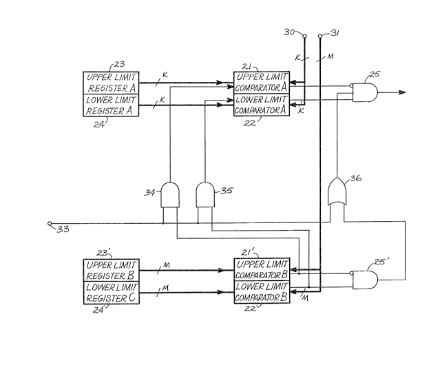
Figure 3 shows a reconfigurable parameter filter
cell constructed in accordance with this invention. It will
be seen that this cell has two sections each corresponding to
the cell of Figure 2. Terminals 30 and 31 are adapted to
receive binary words representing parameters which may, for
example, be a K-bit number at terminal 30 and an M-bit number
at terminal 31, these signals being representative of two
parameters. Alternatively, a (K+M)-bit single number may be
represented by the signals supplied to these terminals, if
greater resolution in signal processing is needed. Terminal
30 is connected to upper and lower limit comparators 21 and 22
as previously described and terminal 31 is similarly connected
to upper and lower limit comparators 21' and 22'. These
comparators function to determine if the signals at terminals
30 and 31 fall within the window limits set by registers 23
and 24 and set by registers 23' and 24'. If the signals do
fall within the windows then AND gates 25 and 25' are enabled
as previously described.
Additional mode selecting circuitry is provided to
control the cell so that the sections act as a single unit. A
terminal 33 is provided to receive the mode control signal and
is connected to one input of each of AND gates 34 and 35 and
to one input of OR gate 36. The other inputs of AND gates 34
and 35 come from the outputs of comparators 21' and 22'. The
~; kh/
.~. . .
.. :~: -- : ,
7~
Gther input to OR gate 36 comes from the output of AND gate
25'. The outputs of AND gates 34 and 35 go to the expansion
inputs oE the upper and lower limit comparators 21 and 22,
respectively.
The action of the mode select signal is as follows:
. . . . _ .
Mode Select Function
_ . . . _ _
0 Independent K and M-bit window comparators
with AND gated output
. . ___ . . ._ .
1 (K~M)-bit window comparator
When the mode select signal is 0 then AND gates 34
and 35 are not enabled and the two halves of the cell operate
independently. If coincidence is detected by AND gate 25'
this coincidence is passed through OR gate 36 to AND gate 35
the ouput of which gives the complete filter output.
When mode select signal is 1 then AND gates 3~ and
35 are enabled and the signal detection limits of comparators
21' and 22' are passed through to comparators 21 and 22 so
that coincidence is indicated only when both comparators 21
20 and 22 and 21' and 22' fall within the appropriate limits.
The output of AND gate 25' plays no part since OR gate 36 is
enabled by the mode select signal.
Thus the application has described a single filter
parameter, preferably implemented as an integrated circuit and
reconfigurable under user control to efficiently handle data
of either high or low precision. The overheads in circuit
complexity or performance to achieve this are minimal.
kh/
- .- . -
:,
,. :- ,, :
,:
.