Note: Descriptions are shown in the official language in which they were submitted.
~26~3fi(3
-- 2 --
l~cK(~RouND OF THE INVENTION
This invention relates to a fast acting solid state AC
circuit hreaker.
Circuit breakers are normally used to protect power
distribl~tion systems by monitoring the current to a load. When
the cllrrent reaches an excessive level which could cause damage
to the line, the breaker opens to prevent the flow of the current
to thereby protect both the line and the load. Prior art circuit
breakers may compr;se a fuse link which overheats as a result of
excessive current and melts thus opening, or may take the form of
a mechanical device which when set provides a current path,
wherein the path is mechanically opened by a reaction of the
breaker to a fault. Fuse link or mechanical circuit breakers,
because of their inherent lag in responding to line faults, do
not immediately open a circuit in response to a fault. This is
acceptable, however, since the line itself can safely handle a
fault for a brief period of time.
A problem exists, however, in the case of power
distribution systems which are supplied by solid state frequency
converters. Such converters are designed to go into a
self-protecting current limiting mode if a fault of a sufficient
magnitude occurs. Because of the slow reaction time of
mechanical circuit breakers, such breakers do not have a chance
to open before the frequency converters enter the self-protecting
current limiting mode. Once this has occurred, the entire system
is without power, and it is impossible to tell where the fault is
since no circuit breaker has tripped to indicate the location of
the fault. In such situations, the fault may be found by opening
the circuit breakers one at a time beginning with those breakers
which are nearest to the frequency converter until the fault is
isolated. This process is very time consuming and is
unacceptable in certain situations.
It would therefore be desirable to provide a fast
acting circuit breaker which would open before a solid state
frequency converter could switch in~o its current limiting mode
1264;~4~9
3 --
so that a load fault would not result in loss of power to the
entire system.
SUMMARY AND OBJECTS OF THE INVE~ITI(`IN
A fast acting solid state AC circuit breaker comprises
a solid state power trans;stor module (PTM) of the ~rlington
type with a damper diode in series with d load circuit. The load
current is sensed in a resistor, and the load current is compared
with preselected threshold current values for equipment turn-on,
load start-up, and steady state conditions. Control circuitry
monitors the comparison to control a driver circuit which turns
the PTM off.
The PTM with suitable driver circuitry is able to be
turned off in less than lO microseconds. This is suffic;ently
fast to prevent a solid state frequency converter wh;ch is
supplying power to the load from switching into a self-protection
current limiting mode in response to a fault, thus removing the
power fro~ the entire line.
In order to allow transients which exceed the normal
steady state current limit to exist on the line without tripping
the circuit breaker, a three level current threshold is utilized
during initial turn-on. Brief current surges are also tolerated
after turn-on to allow additional loads to be added to the line.
It is tllerefore an object of the invention to provide
a fast acting solid state AC circuit breaker.
It is another object of the invention to utilize a
power transistor module of the Darlington type with a damper
diode in a unique manner to provide a fast actin~ AC circuit
breaker.
It is another object of the invention to provide a
fast acting solid state circuit breaker in which the current
waveform to a load is compared to preselected threshold current
values in order to determine if excessive current is being drawn.
It is another object of the invention to provide a
fast acting solid state circuit breaker in which a logic network
opens the breaker to interrupt current to a load if the monitored
lZ643
-- 4 --
current exceeds preselected thresho1d current levels.
It is still another object of the ;nvention to provide
a logic network for a c;rcu;t breaker wh;ch allows steady state
current levels to be exceeded during equ;pment turn-on and load
start-up.
It ;s another object of the invention to provide a
circuit breaker useful in power distribution systems which is
sufficiently fast acting to prevent a solid state frequency
converter from entering a self-protection current limiting mode
in response to a fault in the system.
These and other objects of the invention will become
apparent from the following detailed description taken in
conjunction ~n th the accompanying drawing figures in which
reference numerals used throughout the description designate like
or corresponding parts on the figures.
BRIEF nESCRIPTION OF THE DRAWINGS
Figure l is a schematic drawing of a power generating
and distribution system.
Figure 2 is a ~raph showing maximum permissable inrush
current during system turn-on.
Figure 3 is a graph showing maximum permissable inrush
current during load start-up.
Figures 4A and 4B are schematic dra~n ngs of the fast
acting solid state breaker of the invention.
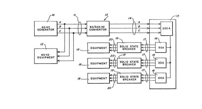
Turning now to Figure l, there is shown a basic
electrical power generation system comprising a 60 hertz
generator lO which supplies three-phase power on lines ll to
general purpose devices 12 such as lights, motors, and 60 hertz
user equipment. The lines 11 are also coupled to a solid state
frequency converter 13 which converts the 60 hertz power from the
generator 10 to DC and then chops the DC power into 400 hertz
three-phase AC power. The three-phase output lines 14 from the
frequency converter 13 are coupled to a switch board 15
comprising a number of mechanical circuit breakers 16 having
selected amperage values. Each mechanical circuit breaker 16 is
1'-'
/
1264369
- 5 -
coupled to three-phase distribution lines 17 which supply power
to the equipment 1~. According to the invention, each
three-phase power distribution line 17 includes a solid state AC
circuit breaker 19 between the mechanical breaker 16 and the
equipment 18.
The frequency converter 13 is a solid state device
which has a self-protect current limitin~ mode. In order for a
circuit breaker 19 downstream of the freguency converters 13 to
be effective, the circuit breaker 19 must open before
self-protect current limiting is reached. The main purpose of
the circuit breaker 19 is to respond to any fault downstream of
the breaker and to open the power line 2n between the circuit
breaker 19 and the failure polnt faster than the frequency
converter 13 can react. This prevents the frequency converter 13
from totally shutting down as a result of a fault.
The solid state circuit breaker 19 comprises a circuit
which includes a power transistor module (PTM). ~Ihen the PTM is
on, current will pass to the equipment 18. When the PTM is off,
the PTM breaks the current path between the equipment 18 and the
upstream switch board 15 and frequency converter 13.
Because of the current capacity of the PTM, and the
characteristics of current flow at turn-on, a plural level
current threshold can be used during turn-on. As an example and
as shown in Figure 2, the turn-on current level for the circuit
breaker is 300 amps for a duration of 10 milliseconds. This
level is then reduced to 150 amps for 25 milliseconds, after
which a set point level of 75 amps is maintained. Curve 21 shows
the envelope of the expected current through the breaker 19
immediately after turn-on. An initial current surge of more than
200 amps decreases to less than 150 amps 10 milliseconds after
turn-on and to less than the set point of 75 amps 25 milliseconds
after turn-on.
Turning now to Figure 3, an in-rush of current through
the breaker 19 caused hy equipment start-up or a momentary
current surge on the line is shown. If the set point current
lZ64369
-- 6 --
level of 75 amps is exceeded, the circuit breaker enters a sur~e
mode in which a maximum of lS0 amps can exist on the line for a
period of 25 milliseconds. After 25 milliseconds, the system
will only tolerate the set point level of 75 amps on the line;
and if the set point level is exceeded, the circuit breaker
treats this condition as a fault and opens the circuit. For a per
iod of lO milliseconds after the 25 millisecond surge mode period
of 150 ampere tolerance, the circuit breaker hnll not re-enter
the 150 amp surge mode. However, after the lO millisecond period
has passed, the surge mode may again be entered. Curve 23 shows
the envelope typical inrush current as a result of a load being
added to the line.
Figures 4A and 4B show a circuit diagram of the solid
state circuit breaker l9 of the invention. It will be understood
that Figure 4B shows circuitry related to the phase A current
on1y and that similar circuitry is required for the phase B and
phase C currents. As shown in Figure 4A, the phase A, phase R,
and phase C currents are all applied to the comparators 41, 42,
and 43.
The breaker 19 includes the power transistor module
(PTM) 25 which is a solid state device comprising a plurality of
transistors in a Darlington conM guration with a damper diode
across the emitter and the collector. The PTM includes a
collector terminal 26, an emitter terminal 27, and a base
terminal 28. A snubber network 24 is coupled across the
collector and emitter terminals 26 and 27 of the PTM to absorb
energy in the PTM at turn-off. The phase A current is coupled to
the collector terminal 26 of the PTM 25, and a control signal for
the PTM is applied to the base terminal 2~ from a an opto
isolator 52 and a driver circuit 53 as more fully explained below.
The emitter terminal 27 of the PTM device is coupled
to a current sensin~ resistor 29 which monitors the current
flowing through the PTM 25 and converts the current to a voltage
which is amplified and used for control purposes.
The voltage across the resistor 29 is monitored by a
lZ64369
-- 7 --
differential amplifier 31 which subtracts any control voltage
present at the ernitter terminal 27 to develop the true voltage
across the current sensing resistor 29. The differential
amplifier 31 also gives the voltage on the resistor 29 a slight
gain. The differential amplifier 31 has an output 32 which is
rectified by a precision full wave rectifier 33. The rectified
output 34 of the full wave rectifier 33 is applied to a driver
circuit 36 which powers a light emitting diode in an opto
isolator 38. The opto isolator 3~ isolates the three phases from
one another to prevent a short circuit and to provide a low-level
signal which is used in the remainder of the breaker circuitry.
A gain stage 39 coupled to the output of the opto isolator 38
applies the signal from the opto isolator to three comparators
41, 42, and 43. The comparators 41, 42, and 43 also receive
similar signals from the respective gain stages (not shown) for
the phase B and phase C ~urrents. Comparator 41 has a threshold
current level of 300 amps, comparator 42 a threshold current
level of 150 amps, and comparator 43 a threshold current level
equal to the set point of 75 amps.
The circuit breaker 19 has three control switches 45
comprising an On switch 67, and Off switch 68, and a Fault Clear
switch 69. To eliminate the contact bounce of the switches 67,
68, and 69, a de-bounce circuit is used for each. The de-bounce
;~ circuits give the circuit breaker a clean turn-on and turn-off.
Closing the On switch 67 causes the signal on the line
50 to go high. Closing the Off switch 6~, or the receipt of a
low signal on the line 66, as more fully explained below, causes
the signa1 on the line 50 to go low. The signal on line 50 is
coupled to one input of an AND gate 51, the output of which
~controls an opto isolator 52. The output of the opto isolator 52
is coupled to the driver 53 for the PTM 25. Closing the Off
switch 68 causes the signal on the output line 50 to be low. The
output of the AND gate 51 then goes low to turn off the opto
isolator 52 and the driver c~rcuit 53 to turn off the PTM. ~he
Fault Clear switch 69 is a lock-out for the On switch 67 which
, ~ ~
., .... ~ .,
':
:
126~3~9
- 8 -
prevents the switch 67 being activated until the Fault Clear
switch 69 has been depressed.
The output of the comparator 41 is high if the voltage
representation of the current applied to the comparator is less
than 300 amps. If the voltage representation of the current
flowing through the PTM exceeds 300 amps, the output of the
comparator 41 will switch from high to low, and the low signal
will be,applied to the AND gate 46. This causes the output of
the AND gate 46 to go low and apply the low to the second input
of the AND gate 51. The output of the AND gate 51 goes low thus
turning off the opto isolator 52 and causing the driver 53 to
turn off the PTM 25. The output of the AND gate 46 is also
coupled to the fault input 66 of the control switches 45. A low
signal on to the fault input 66 causes a fault indicator 65 to be
illuminated. The fault indicator 65 will remain illuminated
until the Fault Clear switch 69 is depressed.
The comparator 42 has a threshold level of 150 amps
and the output of the comparator 42 is high unless the 150-amp
threshold is exceeded. If the output of the comparator 42 Does
low, a low is appl;ed to the OR gate 47, the output of which is
coupled to one input of an AND gate 48. The output of the AND
gate 48 comprises a second input to the AND gate 46. A 10
millisecond one-shot multivibrator 49 comprises a second input to
the OR gate 47. The input of the one-shot multivibrator 49 is
25, coupled to the output line 50 of the control switches 45 and is
triggered when the On switch 67 is activated. The second input
of the AND gate 48 is coupled to the output of an OR gate 57.
A first NAND gate 54, the resistor 58, a capacitor 59,
and a second NAND gate 60 comprise a first input for the OR gate
57. The second input for the OR gate 57 is provided by the
output of an OR gate 56. A 25 millisecond one-shot multivibrator
61 coupled to the output line 50 of the control switches 45
comprises a first input for the OR gate 56. A second 25
milllsecond one-shot multivibrator 62 comprises a second input
for the OR gate 56. The input of the one-shot 62 is coupled to
iZ64369
the output of a 35 m;llisecond one-shot multivibrator 63. The
multivibrator 63 provides an output in response to the falling
edge of a voltage change. The input of the multivibrator 63 is
coupled to the output of an AND gate 64, and the Q-not output of
the multivibrator 63 provides a first input to the AND gate 64.
The second input for the AND gate 64 is provided by the outpùt of
the set point comparator 43.
A delay line is created by the combination of the NA~ID
gates 54 and 60 and the RC combination of the resistor 58 coupled
to a voltage V and the capacitor 59 coupled to ~round. This
combination of elements provides a delay in the output of the
NAND gate 54 in response to an output of the NAND gate 60.
The feedback of the output of one-shot multivibrator
63 to the input of the AND gate 64 provides an inhibiting feature
whereby the one-shot 63 cannot be reset during its 35 millisecond
output period.
~ODE OF OPERATION OF THE PREFERREn EMBODIMENT
A circuit breaker of the instant invention is turned
on by the On switch 67. This causes the output of the control
s~ tches 45 on line 50 to go high. This high is applied to one
of the inputs of AND gate 5l. At this time, the outputs of the
three comparators 4l, 42, and 43 are all high since the threshold
current levels of the comparators are not being exceeded. As a
result, the output of the AND gate 46 is high, the output of AND
gate 51 is high, and each PTM 25 is turned on by its opto
isolator 52 and associated driver circuit 53 (only phase A shown).
The driver circuit 53 for the PTM 25 applies five
volts to the base terminal 28 of the PTM and zero volts to the
emitter terminal 27 of the PTM to turn the PTM on to its
conductive state. Current then flows through the PTM to the
current sensing resistor 29 generating a voltage across the
resistor 29. The differential amplifier 3l detects the voltage
across the resistor 29 and applies the detected waveform 32 to
the precislon full wave rectifier 33. The rectified waveform 34
is applied to the driver 36 for the light emitting diode in the
,,
lZ643~j9
-- 10
opto isolator 38. To maximize the voltage swing of the signal
from the opto isolator 38, the output of the isolator 3R is
coupled to the gain stage 35. The output of ga;n stage 39 is
applied to the three comparators 41, 42, and 43. At the same
time, the output of similar ga;n stages for the phase B and phase
C currents are applied to ~he three comparators 41, 42, and 43.
As long as the threshold levels in each of the comparators 41,
42, and 43 is not exceeded, each comparator has an output which
is high.
At the same time that AND gate 51 is driven high by
output 50 of the control switches 45, the output of each of the
one-shot multivibrators 49 and 61 is driven high by the pulse on
the output 50. This causes the one-shot 49 to give a 10
millisecond pulse and the one-shot 61 to give a 25 millisecond
pulse. The output of the one-shot 49 is applied to one input of
the OR gate 47, the other input of which is connected to the
output of the comparator 42. If the threshold level of 150 amps
of comparator 42 is exceeded during the first 10 milliseconds
after turn-on, the high signal from the one-shot 49 maintains the
output of the OR gate 47 hlgh and thls output is coupled to AND
gate 48. Simultaneously, the 25 millisecond output from one-shot
61 is applied to OR gate 56 which applies a high signal to OR
gate 57, the output of which is coupled to the second input of
AND gate 48. Thus the output of 48 is high and this output is
applied to one input of AND gate 46. At the same time, provided
the input to the comparator 41 does not exceed 300 amps, the
output of comparator 41 remains high; and this output is applied
to the other input of AND gate 46. This causes the output of AND
gate 46 to be high and this output is applied to the input of AND
gate 51.
After 10 milliseconds, the one-shot 49 times out, thus
removing the high from one input from the OR gate 47. At this
time, if the threshold of 150 amps of comparator 42 is not
exceeded, the comparator 42 has a output which is high, which
when coupled to OR gate 47 causes the OR gate 47 to have a high
lZ64369
1,
output which is applied to the input of the AND gate 4~.
Twenty-M ve milliseconds after initial turn-on, the
outpùt of the one-shot 6l goes low. This removes the high
applied to the one input of OR gate 56 and the one input of OR
gate 57. Assuming at this time that the current through the PTM
transistor 25 has decayed to less than set point level of 75
amps, the output of comparator 43 will be high, and this high is
applied to the other input of OR gate 57 causing the output of
the OR gate 57 to be high, the AND gate 48 to have a h;gh output,
the AND gate 46 to have a high output, and the AND gate 5l to
have a high output, thus keeping the opto isolator ~2 on. As
long as the current level at turn-on does not exceed the three
level current threshold shown in Figure 2, the opto isolator 52
through the driver circuit 53 Wlll keep the PTM 25 on.
Assume now for purposes of illustration that the
current through the PTM at the end of lO milliseconds is greater
than l50 amps. This causes the output of comparator 42 to be
low. After lO mllliseconds, the output of multivibrator 49 also
goes low. These two lows are applied to the OR gate 47 causing
the OR gate 47 to have a low output. As a result, the AND gates
48, 46, and 5l have a low output, and the opto isolator 52
through the driver circuit 53 turns the PTM 25 off.
Assume now that imlnediately after turn-on the 300 amp
l~mit of comparator 41 is not exceeded during the first lO
milliseconds of operation and the l50 amp limit of comparator 42
is not exceeded during the next l5 millisecond of operation.
However, the set point level of 75 amps of comparator 43 is
exceeded after the first 25 milliseconds of operation. In this
example, the output of comparator 43 is low, the output of NAND
gate 60 is high, the output of NAND gate 54 is low, and since the
output of one-shot 6l is low after 25 milliseconds, the output of
OR gate 56 is low and the two inputs of OR gate 57 is low. This
causes AND gates 48, 46, and 5l to go low, and the opto isolator
52 through the driver circuit 53 turns the PTM 25 off.
Consider next that the current is flowing through the
1'~64369
- 12 -
PTM 25 and a transient occurs on the line causing the current to
exceed the set point level of 75 amps of the comparator 43 but
not the 150 amp threshold level of comparator 42. In response to
this condition, the output of comparator 43 goes low. The time
S delay of the NAND gates 54 and 60, the resistor 58, and the
capacitor 59 is a few microseconds longer than the reaction time
of the NAND gate 56, the multivibrators 62 and 63, and the AND
gate 64. Thus, when the output of comparator 43 goes low, the
output of NAND gate 57 goes high. The NAND gate 54 then goes
low, but not before the circuit elements 56, 62, 63, and 64 react
to the low condition of comparator 43. When the input to 64 from
comparator 43 goes low, the output of AND gate 64 goes low. This
is detected by the one-shot 63 which is a falling edge device and
the one-shot 63 gives a 35 millisecond pulse in response. The
~urn-on of one-shot 63 causes one-shot 62 to turn on for 25
milliseconds. Thus the output of 62 is high causing the output
of OR gate 56 to be high, the output of OR gate 57 to be high,
and one input to AND gate 48 to be high. If the threshold of 150
amps in comparator 42 is not exceeded, the output of 42 is high,
thus the output of OR gate 47 is high, and the other input of AND
gate 48 is high. This causes the output of 46 to be high, the
output of 51 to be high, and the opto isolator 52 and the PTM 25
remain on.
The feedback of the Q-not output of one-shot 63 into
the input of AND gate 64 prevents the one-shot 63 from being
retriggered on more than once in a 35 millisecond interval.
Thus, the threshold of comparator 43 is overridden by the action
of one-shot 62 only for the first 25 milliseconds of a 35
milllsecond period. After the 25 millisecond period, if the
threshold of comparator 43 is exceeded, the opto isolator 52
through the driver circuit 53 will turn the PTM 25 off. If the
level of comparator 43 is not exceeded for 10 milliseconds after
the 25 millisecond period, the opto isolator 52 remains on. The
one-shot 63 is a retriggerable device. For this reason, the AND
gate 6~ receives the low from the one-shot 63 to block a low
;'
;
'
1~6436g
- l3 -
signal coming from comparator ~3 before the one-shot 63 has an
opportunity to time out.
The driver circuit 53 biases the PTM 25 for maximum
turn-off and speed. When the PTM 25 is on, it is in the
saturated state. If the state is one of deep saturation, a
significant charge is stored within the PTM. Changing the state
of the PTM 25 from conducting to nonconducting requires that the
charge stored in the PTM be removed, and removal of a significant
charge slows down the operation of the circuit breaker. For this
reason, the driver circuit applies 5 volts to the base terminal
28 of the PTM and 0 volts to the emitter terminal 27 to turn the
PTM 25 on. This bias is not enough to put the PTM in a state of
deep saturation, and only a minimum charge is stored in the PTM.
In order to switch the PTM off, the driver circuit applies 5
volts to the emitter and 0 volts to the base to create a negative
potential which draws the charge stored in the PTM so that it may
rapidly switch from on to off.
Having thus described the invention, var;ous
alterations and modifications thereof will be apparent to those
skilled in the art, which modifications and alterations are
intended to be within the scope of the invention as defined in
the appended claims.
~Ihat is claimed is: