Note: Descriptions are shown in the official language in which they were submitted.
126437Z
Television signal processing circuit
The present invention relates to a television signal
processing circuit, and more specifically to a circuit
that is able to process not only standard color television
signals transmitted by broadcasting stations but also
television signals that are at least partly different in
time and phase from such standard signals.
Developments in semiconductor integrated circuit
technology have enable delay means (such as frame memory
or field memory) having a delay time equal to, or longer
than, the vertical scanning period of a television signal
to be realized in a small size and at a low cost. This
has permitted a variety of signal processing circuits to
be put into practice.
According to known signal processing systems, color
television signals are divided into luminance signals and
color difference signals by using a frame memory, or
television signals with interlaced scanning are inter-
polated among the scan lines using a field memory, and
are converted into successive scanned signals. With such
a circuit employing a video memory, such as field memory
or a frame memory having a delay time that is nearly equal
to the vertical scanning period of the television signal
or nearly equal to an integral number of times such
period, there are obtained output signals of high quality
~'
.
i~;437Z
-- 2 --
when the input signals conform to those of a standard
color television system. In processing the output signals
of video tape recorders that are now widely used for
domestic use, however, it is difficult to process the
signals properly utilizing the delay of the field period
of the frame period, since these signals deviate from
standard color television signals. For instance, these
signals have a large jitter and their color subcarrier
frequency is not an integer and a half multiple of the
horizontal scanning frequency. In separating a composite
signal into a luminance and a color difference signal by
using a frame memory, color subcarrier phase difference
between frame periods must be 180 degrees. With video
tape recorders for domestic use, however, the signals are
not so arranged and they are not properly separated into
luminance signals and chrominance signals by inter-frame
processing. In the scanning line interpolation using a
field memory, furthermore, the field period does not
remain constant and the interpolation signals are not
correctly obtained. Accordingly, if signals from a
household video tape recorder are processed by a
processing circuit that has such a video memory as a field
memory or a frame memory, only very deteriorated signals
are obtained.
The principal object of the present invention is to
provide a signal processing circuit having a video memory
which is capable of properly handling not only the
standard color television signals but also non-standard
color television signals, that do not conform with the
standard color television signals that have predetermined
relationships with regard to the line scanning frequency,
the color subcarrier frequency, and phase.
To achieve this objective, there is provided a first
signal processing circuit having a video memory, such as
field memory or frame memory, arranged in parallel with a
second signal processing circuit without a video memory.
~Z6437Z
- 2a ~
Switching means selects the second signal processing
circuit when it is required to process signals that are
not standard.
To this end, the invention consists of a television
signal processing circuit comprising: (1) an input means
Eor receiving a television signal; (2) a first signal
processing circuit which includes a video memory having a
delay time substantially equal to a vertical scanning
period of the television signal or to an integer multiple
thereof, to at least separate a luminance signal and a
chrominance signal of the video signal or to interpolate
the scanning line; (3) a second signal processing circuit
without a video memory, being arranged in parallel with
said first signal processing circuit and being responsive
to said television signal; and (4) selecting means, in
response to a television signal to be processed which does
not conform with the standard color television signal,
selecting the output of said second signal processing
circuit .
~ 3 ~ 1264372
In the drawings:
Figs. l, 2 and 3 are block diagrams which schematically
illustrate the construction of television signal processing
circuits according to embodiments of the present invention;
Fig. 4 is a diagram of a further embodiment in which the
processing circuits of Fig. 3 consist of YC separating circuits;
Fig. 5 is a diagram of a still further embodiment in
which the processing circuits of Fig. 3 consist of scanning
line interpolation circuits;
Figs. 6 and 7 are diagrams of color television receivers
to which the present invention is adapted;
Fig. 8 is a diagram showing the structure of a motion
detector circuit of Fig. 6 according to an embodiment of the
present invention;
Fig. 9 is a diagram showing the structure of a motion
detector circuit of Fig. 6 according to a further embodiment
of the present invention;
Fig. 10 is a circuit diagram of a scanning line inter-
polation circuit of Fig. 6 according to an embodiment of the
present invention; and
Fig. 11 is a diagram showing the structure of a scanning
line interpolation circuit, and the vertical and horizontal
synchronizing signal separating circuits of Fig. 6 according
to another embodiment of the present invention.
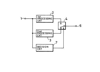
Fig. l is a diagram that schematically illustrates a
structure according to an embodiment of the present invention,
wherein a television signal received at a terminal l is fed to
a first signal processing circuit 2 having a video memory and
to a second signal processing circuit 3 without a video memory.
As will be described later in detail, the video memory has a
delay time that is nearly equal to the vertical scanning period
of the television signal or which is nearly equal to an
integral number of times such period.
Outputs of the circuits 2 and 3 are selected by a switch-
3S ing circuit 4. When signals that are not in conformity withstandard color television signals are to be processed, the
_ 4 ~26437Z
switching circuit 4 is controlled by a control signal
applied to a terminal 5 to select the output of circuit
3. When the input signal is standard, the output of the
circuit 2 is selected and passed to an output terminal 6.
Fig. 2 illustrates an embodiment wherein the circuits
2, 3 and 4 are the same as those of Fig. 1, but there is
also a decision circuit 7 which determines whether the
signal is standard or not, in accordance with whether
there is a predetermined offset relationship between the
color subcarrier frequency and the scanning frequency, or
if there is a change in time in the field period or in the
frame period.
Fig. 3 illustrates another embodiment of the present
invention wherein circuits 2 and 3 are the same as those
of Figs. 1 and 2. The outputs of these circuits 2 and 3
are fed to coefficient circuits 8 and 9 where they are
respectively multiplied by k and (l-k) and added in an
adder circuit 11, the resultant output appearing on
terminal 6. Symbol k denotes a motion coefficient which
varies between 0 and 1 depending upon the presence or
absence of motion. A motion detecting circuit 10 extracts
motion information that is contained in the television
signal and converts it into the motion coefficient k.
In a portion of a still picture where there is no motion,
the coefficient k approaches 1 and the output signal of
the first processing circuit 2 occupies most of the final
output. In a moving area where there is a large change,
the coefficient k approaches 0 and the final output signal
comes mostly from the second processing circuit 3. When
the signal to be processed is not standard, the motion
detecting circuit 10 is controlled by a control signal
appearing on a terminal 12 to force the motion coefficient
k to become 0, so that the output of the circuit 3 appears
at the terminal 6. The signal on the terminal 12 can be a
signal that is manually designated, or a signal that
126437z
-- 5 --
adapts to an input television siqnal entered through a
particular terminal, or an output signal of the decision
circuit 7 of Fiq. 2. The same is true for the signal
applied to the terminal 5 of Fig. 1.
Fig. 4 is a block diagram that provides more details
of the embodiment of Fig. 3 in relation to a motion-
adaptive YC separating circuit, i.e., a circuit that
separates a color television signal of the NTSC system
into a luminance signal Y and a modulated chrominance
signal C by using a frame memory and a line memory.
In a color television signal of the NTSC system, the
polarity of the modulated chrominance signal C is inverted
after every hori~ontal scanning period H and also relative
to the signal on a scanning line on the same position of
the screen one frame earlier, i.e., 525 H. If the input
television signal is denoted by XO, a signal delayed by lH
by the line memory is denoted by X-l, and a signal delayed
by 525H by the frame memory is denoted by X-525, a
modulated chrominance signal Cl is extracted by the first
processing circuit 2 as expressed by,
XO - X-525 . HBPF ----(1
Cl = 2
where HBPF denotes the transmission characteristics of
a band-pass filter which extracts signals in the
modulated chrominance signal band.
The second processing circuit 3, on the other hand,
extracts a modulated chrominance signal C2 as expressed by,
C2 XO - X-l . HBPF ----(2)
By adding proportions of equations (1) and (2) in the
following manner, therefore, a desired modulated chrominance
signal C is obtained as,
C = k . Cl + (1 - k) C2
= k . XO - X-525 . HBPF
+ (1 - k) . XO - X-l . EIBPF
= XO - [ (X - 525 - X - 1) . k + X-l] . HBPF ----(3)
:~264372
-- 6 --
Equation (3) is calculated by the circuit of Fig. 4 to
generate a modulated chrominance signal that is then
subtracted from the NTSC signal to obtain a luminance
signal Y. That is, an NTSC signal xO at input terminal 13
is delayed by lH in a line memory 14 to obtain the signal
X-l, and is delayed by 525H in a frame memory 15 to obtain
the signal X-525. Outputs of the memories 14 and 15 are
subtracted from each other in a circuit 16, the subtracted
result being multiplied by k in a circuit 17, the output
of which is added to that of the memory 14 in a circuit
18, thereby to achieve the portion in square brackets in
equation (3). In a subtracting circuit 19 the output of
the adder circuit 18 is subtracted from the input signal
XO, and the result is halved in a circuit 20 and fed to a
band-pass filter 21 to yield at a terminal 25 the desired
modulated chrominance signal C in accordance with equation
(3~. A desired luminance signal Y can be obtained at
terminal 24 by subtracting the modulated chrominance
signal C in a circuit 23 from a signal that is obtained by
delaying the input NTSC signal by a delay circuit 22 by a
time equal to a delay time of the band-pass filter 21.
A frame-difference signal is obtained by a subtracting
circuit 26, and a low-frequency component thereof is
extracted by a low-pass filter 27. An absolute value of
the low-frequency component through an absolute value
circuit 28 represents the motion information in the
television signal which is proportional to the luminance
change between the frame period.
If a video signal on the terminal 13 is from a
household video tape recorder, it contains jitter due to
mechanical features in the VTR. Therefore, the phase
relationship of the opposite polarities is no longer
correctly maintained with respect to alternate frames.
Hence, an added signal between frames is observed in the
burst portion. If there is no such added signal, it is an
126437Z
indication that the signal is in conformity with the
standard color television system of NTSC. l~ the added
signal is not greater than a threshold value, it is
apparent that the input signal is from a household VTR.
In the embodiment of Fig. 4, the added signal between the
frames is ~alculated by an adder circuit 31 and is fed to
a band-pass filter 32 to extract the components of the
subcarrier signals. A gate circuit 33 then gates the
burst portion only from a gate signal obtained by a burst
gate circuit 37 which extracts a signal that indicates the
burst signal period among the input signals. The absolute
value thereof is found in a circuit 34 and is accumulated
during a burst period by an accumulator 35. This accum-
ulated value is then compared by a threshold circuit 36
with a predetermined threshold value. If a signal greater
than the threshold value is detected, the register 30 is
reset, and the motion coefficient k is forced to become
0. The operation of ~C separation can thus be realized as
intra-field processing without using the output of the
frame memory.
Fig. 5 is a diagram which illustrates the circuit of
Fig. 3 according to a further embodiment of the present
invention adopted to a signal processing circuit that
converts the interlaced-scanned television signal into
successive scanned television signals by using the motion
adoptive line interpolation. In Fig. 5, the interlaced
television signal is received at a terminal 38 and is also
fed to a line memory 39 that delays it by lH and to a
field memory 42 that delays it by 263H. Relative to the
present input signal ZO, a signal Z' of an interpolated
scanning line just above is found by the following motion-
adaptive calculation. The first signal processing circuit
prepares an interpolated signal Z'l relying upon a signal
Z-263 of a previous field delayed by 263H on a scanning
line of the same position, i.e.,
Z'l = Z-263 ----(4)
In the second signal processing circuit, on the other
hand, an interpolated signal Z'2 is prepared relying upon an
~26437;~:
average value of the present signal ZO and a signal Z-l ~elayed
by lH, i.e.,
Z'2 = ZO + Z-l -----(5)
The interpolated signal Z' is found by mixing Z'l and Z'2
together with the motion coefficient k as was explained in the
embodiment of Fig. 4, i.e.,
Z' = kZ'l + tl - k) Z'2
= k(z-263 - Zo + Z-l + zO + Z-l -----(6)
2 ) 2
In Fig. 5, an adder circuit 40, a one-half coefficient
circuit 41, a subtracting circuit 43, a coefficient circuit 44,
and an adder circuit 45 perform the arithmetic operation of
equation (6), being controlled by the motion coefficient k
that appears on a register 50, whereby to obtain the inter-
polated signal Z'. The signal ZO of the present scanning line
and the signal æ ~ of the interpolating scanning line are com-
pressed on their time axes into one-half by time compressing
circuits 46 and 47. A switching circuit 48 is switched to a
scanning line unit in which the time is compressed, whereby
there are obtained at a terminal 49 signals having a horizontal
scanning period that is reduced to one-half, the signals suc-
cessively scanning the whole scanning lines during the fieldperiod of the input television signals.
When the television signal received at the terminal 38
is from a household VTR having a jitter in the time axis, i.e.,
a non-standard television signal, the register 50 is reset and
the motion coefficient is forcibly caused to become 0, so that
a signal of average line interpolation is obtained as an inter-
polated signal. According to this embodiment, the presence or
1264372
_ 9
absence of the change in time axis is determined as
described below A start signal in the vertical
synchronization of the television signal ZO is extracted
by a pick-up circuit 51, the period of the vertical
synchronizing signals is measured by a counter 52 which
operates on clock signals of a sampling frequency, and the
measured value of the vertical scanning period is supplied
from a gate circuit 53 to a decision circuit 54 which
renders the decision that the signal is in conformity with
the standard television system when the measured value is
equal to a predetermined value. When it is not equal to
the predetermined value, the decision circuit 54 decides
that the signal has a large change in time axis, which is
not in conformity with the standard system, and resets the
register 50.
The decision method of Fig. 5 can also be adopted to
monochromatic television s~gnals and color television
signals of other systems (such as signals obtained by time-
compressing the component signals and color difference
signals and time-multiplexing them upon luminance signals)
in addition to color television signals of a standard
system such as the NTSC system.
When it is decided that the signal does not conform to
the standard system, as a result of a decision by the
decision circuit of the embodiment of Fig. 4 or the
decision circuit of the embodiment of Fig. 5, which are
arranged in parallel with each other, the second intra-
field processing circuit should be employed in order to
realize a signal processing circuit that can cope with a
wide range of signal sources.
As will be obvious from the structure of the
embodiment, the first and second signal processing circuits
126437Z
-- 10 --
share some common portions, and only those portions that
are substantially different will be placed in parallel to
simplify the circuit.
The embodiments of Figs. 2, 4 and 5 are provided with
a decision circuit to automatically decide whether the
input television signals are standard or not. However, it
is also possible to provide a plurality of pairs of input
terminals whereby to decide that a signal supplied to
particular terminals is the one that is not standard, or a
switching signal can be manually applied.
As an example of a signal processing circuit having a
video memory, the present invention has dealt with a YC
separating circuit and a circuit for converting the inter-
laced scanning signal into successive scanning signals.
The present invention, however, is in no way limited
thereto, but can be adopted to coding apparatus for inter-
frame coding and inter-field coding, as well as to general
signal processing circuits having video memories such as
noise-removing circuits in general.
Although the embodiments (Figs. 4 and 5) of the present
invention have dealt with television signals of the NTSC
system, it will be obvious that the invention can be
adopted to any other system (such as PAL, SECAM, or the
like).
Fig. 6 is a block diagram illustrating the structure
of a color television signal processing circuit according
to a further embodiment of the present invention.
In Fig. 6, composite color television signals of the
NTSC system are supplied to an input terminal 1 and are
digitized by an analog-to-digital converter 60. The input
signals are also fed to a clock generator 61 which produces
clock signals of which the phase is locked to color burst
signals of the input signals, the clock signals being
IZ64372
supplied to the converter 60 and the like. The output of
the converter 60 is fed to a motion-adaptive YC separating
circuit 63 which utilizes the frame memory and the line
memory, and to a motion detecting circuit 64. The
separated luminance signals Y are fed to a motion-adaptive
scanning line interpolation circuit 65 which utilizes the
field memory and the line memory, and are converted into
successive double scanned signals. The separated modulated
chrominance signals C are demodulated by a demodulating
circuit 66 into color difference signals, and are converted
into double scanned successive scanning signals by a
scanning line interpolation circuit 67 which utilizes the
line memory. The successive scanning signals obtained are
returned to analog signals by digital-to-analog converters
68, 69, converted through a matrix circuit 70 into signals
of three primary colors (red R, green G and blue B), and
are fed to a display device 73.
Horizontal synchronizing signals HD are separated by a
horizontal synchronizing signal separating circuit 71 from
the outputs of the converter 68 after the double scanning,
and are supplied to the display device 73.
A vertical synchronizing signal separating circuit 72
separates a vertical synchronizing signal VD from the Y
signal that is separated by the YC separating circuit 63,
and supplies it to the display.
The motion-adaptive YC separating circuit 63, scanning
line interpolation circuit 65, motion detecting circuit
64, and a decision circuit 62 that decides whether the
input television signals are standard or non-standard, are
the same as those used in the embodiments of Figs. 4 and 5.
The non-standard signals can be discriminated (1) by
the above-mentioned method whic'n forcibly assumes the
126437z
- 12 -
non-standard signal mode relying upon manual operation,
(2) by a method that provides input terminals for
exclusively receiving non-standard signals, and assumes
the non-standard signal mode when a signal is input
thereto, and (3) by a method that monitors a synchronizing
signal in the input color television signals and assumes
the non-standard signal mode when the phase changes between
the frames (specifically, when the number of clocks of the
frame period is different from a predetermined number of
clocks), or a method that monitors an added signal between
the lines of color burst portion and which, when a signal
of a color subcarrier wave component is greater than a
predetermined value indicating that an offset relationship
no longer exists, determines the presence or absence of
the signal and uses it as a decision signal. The decision
circuit 62 of Fig. 6 corresponds to method (3).
The signal is delayed in the YC separating circuit 63
or in the scanning line interpolation circuit 65 due to the
processing. Therefore, a time deviation develops between
the video signal and the synchronizing signal, if the
synchronizing signal (particularly, the horizontal
synchronizing signal), that drives the display monitor 14,
is picked up from the input signals and is supplied to the
monitor 73. This deviation does not affect the reproduced
picture when standard signals without jitter in time are
being inputted. When non-standard signals are being
inputted, on the other hand, the deviation is accompanied
by a jitter in time and results in a swing of the picture
to the right or left. To avoid this according to the
embodiment of Fig. 6, the converter 60 digitizes the
signals inclusive of the synchronizing signals, and the
circuit 71 separates horizontal synchronizing signals HD
from the output signals of the converter 68 after they
lZ64372
- 13 -
have been double scanned, in order to drive the display
monitor 73. Therefore, the video signals and the
horizontal synchronizing signals supplied to the display
monitor have the same jitter in time. Thus this jitter is
cancelled and the picture is reproduced correctly.
Fig. 7 is a diagram illustrating the structure of a YC
separating circuit in a television signal processing
circuit according to a further embodiment of the present
invention, wherein portions that correspond to those of
Fig 6 are denoted by the same reference numerals.
This embodiment is particularly effective when a clock
signal, the phase of which is locked to the horizontal
synchronzing siqnal of the input television signal, is to
be used. The clock generator 61 of Fig. 7 generates such
a clock signal.
If the circuit 62 decides that the input television
signal is standard, switches 74 and 75 are controlled to
select outputs Y and C of the circuit 63, the structure of
which is the same as in Fig. ~.
If the circut 62 decides that the input television
signal is non-standard, switches 74 and 75 are controlled
to selected outputs Y' and C' of the circuit 63'. The
luminance signal Y' is generated by a low-pass filter 76
from the input signal and the modulated color signal C' is
generated by a band-pass filter 77. In the case of non-
standard signals, such as from a household video tape
recorder, there is no offset relationship whereby the
phase of the color subcarrier signal is inverted between
the lines. Therefore, the YC separation is effected by
line processing using simply a low-pass filter or a
band-pass filter.
When the input signals are from a household video tape
recorder, the signal before the frame period or the field
period is not utilizable, since there is a jitter in the
1264372
- 13a -
time axis. This can be realized by setting the coe~ficient
k to "0" (motion picture mode). Fig. 8 illustrates the
structure of the motion detecting circuit 6. A motion data
signal My of a low-frequency component of a brightness
signal is obtained by finding the absolute value of a low-
frequency component having a frame difference from an input
color television signal XO and a signal X-525 delayed by a
frame memory 80, using a subtracting circuit 81, a low-pass
filter 82 and an absolute value circuit 83. On the other
hand, an absolute frame difference signal of a component of
a modulated color signal band is obtained through band-pass
filters 84 and 85, absolute value circuits 86 and 87, and
a subtracting circuit 88. When this signal is demodulated
by an absolute value circuit 93 and a low-pass filter 89,
there is obtained a motion data signal Mc of the color
difference signal. The two signals My and Mc are added
together in an adder circuit 90, and the resulting signal
is converted by a circuit 91 into a motion coefficient k.
If the input signal is non-standard, such as one from a
household video tape recorder, the motion coefficient is
forced to become "O", being controlled by a decision
signal S (explained later), and the YC separating circuit
63 and, as required, the scanning line interpolation
circit 65 are caused by a switching circuit 92 to assume
the inter-field processing mode.
Fig. 9 is a circuit diagram of the motion detecting
circuit 64 according to another embodiment which modifies the
output side of blocks 83, 89 of Fig. 8, the input side being
126437;~
- 19 -
the same as in Fig. 8. The absolute value circuit 83 produces
a motion data signal My of a low-frequency component of the
brightness signal, and a low-pass filter 89 produces a motion
data signal Mc of the color difference signal. When the input
signal is standard, a switch 94 is connected in its upper posi-
tion by an output from the decision circuit 62, and an adder
90 produces the sum of signals My and Mc, which is converted
into a motion coefficient by a circuit 91. When the input sig-
nal is non-standard, the modulated color signal does not have
a condition that the polarity is inverted between the frames,
and it is not appropriate to use the motion data Mc. Therefore,
the switch 94 is connected in its lower position by the decision
signal S, so that the signal Mc fed to the adder circuit 90 is
forced to assume the value "O" (no motion).
When a clock signal is to be locked in phase with the hori-
zontal scanning period of the input television signals, the
position of each of the picture elements always remains constant
relative to the picture despite the presence of jitter-
in the time axis. The jitter components are thus cancelled.
Therefore, attention need simply be given to the fact that the
phase of the modulated color signal does not establish an offset
relationship between the lines. The YC separation is therefore
performed by the interline processing, the motion coefficient
is generated by a frame difference signal of a low-frequency
2S component of the brightness signal, and a scanning line inter-
polation of the motion-adaptive type can be performed using a
field memory as in the case of standard television signals.
Fig. 10 illustrates the structure of the motion-adaptive
scanning line interpolation circuit 65 according to another
embodiment. In Fig. 10, the signal processing circuit consists
of a circuit 65-1 which obtains a first signal V1 of an inter-
polated scanning line from the input television signal VI~ and
obtains from this input signal VI a second signal V2 that is
delayed by 262H (H denotes a horizontal scanning period) that
is nearly equal to a vertical scanning period, and another
circuit 65-2 which compresses the first and second signals Vl
126437z
- 15 -
and v2 into one-half in time, and obtains a time-multiplexed
output television signal VO wlth the scanning line as a unit.
In the signal processing circuit 65-1, the input signal VI is
fed to delay circuits 101, 102 and 103 that have delay times
of 262H, lH and 262H, respectively, and which are connected in
cascade, and provides an average value Vt of signals delayed
by one frame (525H) with respect to the signal VI obtained
through an adder circuit 104 and a coefficient circuit 105.
Further, an average value Vs of the input and output signals
of the delay circuit 102 having a delay time of lH is obtained
through an adder circuit 107 and a coefficient circuit 108.
The two average value signals Vt and Vs are mixed through co-
efficient circuits 106, 109 and an adder circuit 120, the mix-
ing ratic being controlled by the motion coefficient k (O<k<l)
which represents the motion data of a subject picked up by a
motion detecting circuit (not shown). The first signal Vl
which is a signal of the interpolated scanning line is given by,
Vl = kVt + (1 - k)Vs
The second signal V2 is the one that is obtained by delaying
the input signal by 262H by the delay circuit 101. In the cir-
cuit 65-2, the two signals Vl and V2 are supplied to memories
110 and 111, each having a capacity of lH, and are read out at
double speed to compress the time into one-half. A switching
circuit 112 is switched into the scanning line unit, and the
signals are returned by a digital-to-analog circuit 113 back
to analog television signals. An output signal VO is thus
supplied to the display device is obtained from a terminal 116.
When the input TV signal VI is non-standard, e.g., from
a video tape recorder having large jitter, the aforementioned
motion coefficient k is forced to assume 0. The signal Vt
which is an average value of scanning lines of the preceding
and succeeding fields, is then no longer utilizable, and the
average value Vs of the upper and lower scanning lines that
126437z
- 15 -
are close in time to each other, is produced as the signal Vl.
Therefore, the average signal of the upper and lower display-
ed scanning lines is displayed as the picture. The synchroni-
zing signal works to display the above signal correctly on the
display unit. However, since the signal Vl consists of an
average value of the upper and lower scanning lines, the wave-
form of the vertical synchronizing signal is disturbed, and
it becomes difficult to generate the vertical synchronizing
signal. The embodiment of Fig. 10 is designed to solve this
problem, since the horizontal synchronizing signal HD is only
separated from the output signal VO by the synchronizing sig-
nal separating circuit 114, and the vertical synchronizing
signal VD is separated by the first synchronizing signal
separating circuit 115 from the second output signal V2 of the
circuit 65-1. The signal V2 is the one that is obtained by
simply delaying the input TV signal VI by the vertical scan-
ning period. Therefore, no disturbance is contained in the
vertically synchronized portion, and the vertically synchroni-
zing signal VD can be easily generated.
Fig. 11 illustrates a signal processing circuit similar
to that of Fig. 10 to generate synchronizing signals accord-
ing to a further embodiment. The second signal V2 of the
circuit 65-1 which is delayed, is returned to analog form by a
digital-to-analog converter circuit 121, and the horizontal
synchronizing signal HD' and the vertical synchronizing signal
VD are separated by a synchronizing signal separating circuit
122. If the signal HD' is double-scanned by a frequency multi-
plying circuit 123, the desired horizontal synchronizing sig-
nal HD is obtained.
When the circuit of Fig. 10 or 11 is used as t~e circuit
65 of Fig. 6, the input signal VI is a separated luminance
signal. The input signal VI, however, can be a composite
television signal that contains a synchronizing signal, or can
be a component signal of red (R?, blue (B) and green (G) that
contains a synchronizing signal.
When the input television signal VI consists of an analog
126~37z
- 17 -
signal, furthermore, the analog-to-digital converter must be
provided.
In the embodiment of Fig. 10, the horizontal synchroniziny
signal HD is generated from the output side of the converter
113. However, it is also possible to separate it digitally
from the input side of the converter 113. When the signal is
digitally extracted, nowever, jitter can easily take place in
the horizontal direction due to distortion caused by sampling.
In the case of the vertical synchronizing signal VD having a
long period, the effect of jitter by sampling can be neglected,
and the circuit 115 can be a digital circuit.