Note: Descriptions are shown in the official language in which they were submitted.
1269~38~
-- 1 --
SEMICONDUCTOR DEVICE
sAcKGRouND OF THE INVENTION
l) Field Q f the Invention
The present invention relates to a semicon-
ductor device. More particularly, it relates to a
package structure for housing a ultra-high frequency
semiconductor chip.
The package of the ultra-high frequency
semiconductor device comprising, for example, a gallium
arsenic field effect transistor (FET) used in a giga
hertz frequency band should be constructed so that the
function of the highly improved semiconductor chip is
not degraded and that the package is easily made.
2) Description of the Related Art
A semiconductor device utilizing an FET chip
comprises a package for housing the chip, an input lead
piece, an output lead piece, and two earth lead pieces
for grounding and power supply.
The conventional semiconductor device known to
the inventor comprises a semiconductor chip mounted on a
ceramic base plate, four ceramic side walls rectangularly
arranged surrounding the semiconductor chip, a cap
secured to the upper edges of the side walls via a
metallized film, an input lead piece and an output lead
piece extending from each of the pair of opposing side
walls, and two earth lead pieces extending from the
other pair of opposing side walls. The earth lead
pieces are connected to the semiconductor chip through a
metallized film coated on the base plate and side walls.
In the above conventional semiconductor device
structure, a satisfactory grounding function has not
been obtained since the metallized film is very thin.
Also, the characteristic of the device is unstable since
unnecessary noise signals are transmitted from the input
lead piece to the output lead piece or vice versa
through the metallized film coated on the upper edges of
2 1264380
the side walls.
SUMMARY OF THE INVENTION
The present invention aims to obviate the above
mentioned drawbacks of the conventional semiconductor
device by providing a semiconductor device which achieves
a satisfactory grounding function by reducing the
inductance of the grounding line, and which has a stable
characteristic inhibiting unnecessary transmittance of
signals from the input terminal to the output terminal or
vice versa, bypassing the semiconductor chip.
A semiconductor device in accordance with the
present invention comprises:
a base plate for mounting a semiconductor
chip;
side walls disposed on the base plate to
surround the semiconductor chip;
an input lead piece and an output lead piece,
both being connected to the semiconductor chip and
extending outward from the side walls; and
at least one earth lead piece extending
outward from the side wall between the positions from
where the input and output lead pieces are taken out,
characterized in that the side walls at the positions
from where the input and output lead pieces are taken
out are made of electric insulation material and that
the side wall at the position from where the earth lead
piece is taken out is made of metal integral with a
bonding terminal extending inward of the side wall and
the outer earth lead piece as one body.
Brief Description of the Drawings
Figure 1 shows a semiconductor device according to
the present invention, wherein (a) is a plan view
and (b) and (c) are partial sectional views thereof;
Figure 2 is a perspective view of the semiconductor
device of Fig. l;
Figure 3 is an equivalent circuit diagram of the
semiconductor device of Fig. l;
:
~"
1264380
-- 3 --
Figure 4 shows another embodiment of the semicon-
ductor device according to the present invention in a
way similar to Fig. 1;
Figure 5 is a perspective view of the semiconductor
device of Fig. 4;
Figure 6 shows still another embodiment of the
semiconductor device according to the present invention
in a way similar to Fig. l;
Figure 7 shows a related conventional semiconductor
device in a way similar to Fig. l; and
Figure 8 is an equivalent circuit diagram of the
semiconductor device of Fig. 7.
Description of the Preferred Embodiments
Embodiments of the present invention will now be
described with reference to the drawings and in
comparison with the related art known to the inventor.
A conventional pac~age structure utilized for an
ultra-high frequency semiconductor device is illustrated
in Fig. 7, wherein (a) is a plan view and (b) and (c)
are partial sectional views.
In the drawing, numeral 1 designates a rectangular
ceramic base plate. A side wall 2 having a continuous
rectangular frame shape in the plan view is disposed on
the base plate 1 along the four edges thereof. Metal-
lized films 3 are coated on the opposing outer surfacesof the side wall 2 and the base plate 1. The metallized
films 3 are made of, for sample, tungsten. Further
metallized films 4 for leading input and output signals
are coated on the further opposing outer surfaces of the
base plate 1. The upper edge surface of the side wall 2
is coated with a metallized film 5 in a rectangular
frame shape in plan view, for sealing a cap 11. The
metallized film 5 is connected to the metallized films 3.
The metallized films 4 and 5 are made of the same
material as the metallized film 3. The base plate 1,
the side wall 2, and the metallized film 3 to 5 simul-
taneously undergo sintering process to form a container
,: :
_ 4 _ lZ643~0
box shaped base unit 6.
Outer lead pieces 7 and input and output pieces 8
of metal such as Xovar (Westinghouse Electric Corp.) are
brazed to the bottom edges of the base plate 1 through
the metallized films 3 and 4 to form a package for the
semiconductor device. The lead pieces 7 and 8 are
plated with gold.
A semiconductor chip C is bonded on the base
plate 1 at the center thereof and connected through
wires W to metallized films 9 and 10 disposed on the
base plate 1 projecting inside of the side wall 2 and
connected to the metallized films 3 and 4, respectively,
to serve as inner bonding terminals. After that, the
cap 11 of, for example, Kovar is brazed on the upper
edge surface of the side wall 2 via the metallized
film 5 to seal the package.
- In the above mentioned structure, the semiconductor
chip C is connected to the outer earth lead pieces 7
through the metallized films 3 and 9, which are very
thin. Conventionally, the metallized film 3 has a
thickness of several ~m. Therefore, in a high frequency
band, the grounding function of the earth lead pieces 7
through the metallized films 3 and 9 is degraded due to
the inductance of the metallized films 3 and 9. Accord-
ingly, problems have occurred with the conventionalsemiconductor device in that a desired gain is not
obtained when the frequency is made higher and that a
stable function is not achieved due to the feedback
signals from the output terminal to the input terminal
through the metallized film 5 and the cap 11.
This is further described with reference to Fig. 8,
which is an equivalent circuit diagram of the semicon-
ductor device of Fig. 7.
Input terminal A and output terminal B are connected
to the semiconductor chip C such as an FET. The side
wall 2 serves as a condenser and the metallized film 5
coated on the side wall 2 serves as an inductance coil,
* Trade Mark
lZ6~380
-- 5 --
so that a circuit is formed bypassing the semicanductor
chip C from the input terminal A to the output terminal B
to transmit unnecessary noise signals, which degrade the
characteristic of the transistor. The earth lead
piece 7 is connected to the middle portion of the
metallized film 5 through the metallized film 3 coated
on the outer face of the side wall 2. The metallized
film 3 is very thin, as mentioned before, and the
inductance thereof is very large, so that it cannot
completely lead the unnecessary signals to the ground to
prevent the transmittance of the signals from the input
terminal A to the output terminal B or vice versa.
The terminal for grounding of the semiconductor
chip C is connected to the ground through the metallized
films 3 and 9 and the earth lead piece 7, in which the
metallized films 3 and 9 are very thin, as mentioned
before, and the inductance thereof is very large, which
adversely influences the grounding function.
Such drawbacks are obviated in a semiconductor
device according to the present invention and illustrated
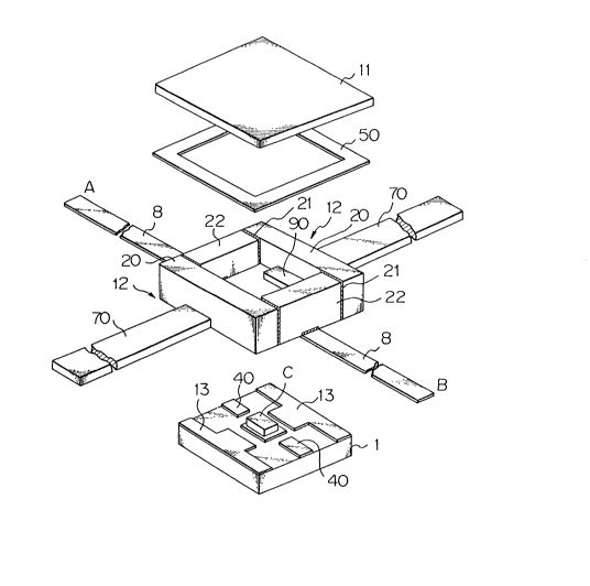
in Figs. 1 and 2. A primary difference of the package
structure of Fig. 1 over that of Fig. 7 resides in that
the side wall on the side from which the outer lead
piece 7 for grounding extends is formed by metal as a
metal wall 20, which is integral with an outer earth
lead piece and an inner bonding terminal.
In Figs. 1 and 2, numeral 1 designates a rectangular
base plate made of electric insulation material such as
ceramic. Metal walls 20 are disposed on the opposing
sides of the rectangular base plate 1. The metal
walIs 20 are made of e.g. oxygen-free copper. Ceramic
side walls 22 are disposed on the other opposing sides
of the rectangular base plate 1. From the ceramic side
walls 22, input and output outer lead pieces 8 extend
outward. The metal wall 20 is formed integral with an
outer earth lead piece 70 and an inner bonding
terminal 90 as one body to form an earth terminal
:::
,~
l Z64~B~
block 12. Input and output metallized films 40 are
formed on the base plate 1 to connect the semiconductor
chip C to the input and output lead pieces 8 through
wires W. A rectangular ring seal 50 of metal such as
Kovar is disposed on the upper edges of the metal
walls 20 and the ceramic walls 22 for sealing a cap 11.
The seal 50 corresponds to the metallized film 5 of
Fig. 7. The metallic earth terminal block 12 is bonded
to the base plate 1 through a metallized film 13. The
metal wall 20 and the ceramic wall 22 are bonded together
through a metallized fi;m 21.
The base plate 1, the ceramic walls 22 and metal-
lized films 40, 21, 13 undergo a sintering process
together to form a base unit. The earth terminal
blocks 12 are brazed at a predetermined position on the
unit. Also, the metal seal ring 50 and input and output
outer lead pieces 8 are brazed at a predetermined
position on the base unit to form a package. Each outer
lead piece is plated with gold.
A semiconductor chip C is mounted on the base
plate 1 in a same manner as depicted in Fig. 7 except
that the inner bonding terminal 9 of Fig. 7 is replaced
by a thickened inner bonding terminal 90. After the
semiconductor chip C is housed within the package, the
cap 11 is brazed onto the rectangular metal ring 50 to
seal the package.
In this package structure, the outer earth lead
piece 70, the inner bonding terminal 90, and the metal
ring 50 for sealing the cap are interconnected through
the thick metal side wall 20 having very little
inductance compared with the structure of Fig. 7, which
makes it possible to achieve a satisfactory grounding
function at a high frequency. For example, if the
maximum usab~e frequency in the structure of Fig. 7 is
about 12 GHz, it is possible to increase the maximum
frequency to about 20 GHz by adopting the structure of
Figs. 1 and 2.
. ~
. ;
1264~30
- 7 -
An equivalent circuit diagram of the semiconductor
device of Figs. 1 and 2 is illustrated in Fig. 3. As
can be seen from the diagram, in comparison with the
diagram of Fig. 8, the unnecessary signals transmitted
from the input terminal A to the output terminal B or
vice versa through the metal ring 50 which constitutes a
bypass circuit are almost completely lead to the ground
in the middle of the metal ring S0 since the metal
ring 50 is connected to the ground through a thic~ metal
side wall 20 which has almost no inductance, thus
inhibiting the transmittance of signals between the
terminals A and B through the bypass circuit, which
stabilizes the characteristic of the semiconductor
device. Also, the earth terminal of the transistor
chip C is lead to the ground through the thick inner
bonding terminal 90, the metal side wall 20, and outer
lead piece 70 which are made integrally as one metal
block having almost no inductance, thus achieving a
satisfactory and reliable grounding function.
With the structure of Figs. 1 and 2, when assembling
the semiconductor device, a pair of earth terminal
blocks 12 composed of the inner terminal 90, the side
~-~ wall 20, and the outer lead piece 70 is disposed on the
base plate 1, the two blocks 12 being aligned with each
other at a predetermined position. The actual dimension
of the semiconductor device is usually very small, for
instance, the package container box is 1.8 mm square,
the length of each lead piece is about 3 mm, the height
of the package is about 0.7 mm. The assembling operation
of such minute parts in alignment with each other is not
easy.
Figures 4 and 5 show another embodiment of the
present invention wherein a further improvement resides
~; in that the package is easily assembled. In this
embodiment, the two opposing metal side walls 20 are
interconnected through the same metal connecting
~ bridges 20a above the ceramic side walls 22 to form an
.',..~,:, ~ ~
, ~
:: '
lZ6~;~80
- 8 -
earth terminal block 30 as one metal body.
The ceramic side wall 22 from which the input or
output lead piece 8 extends must have a sufficient
height for reliable insulation, to stabilize the charac-
teristic of the semiconductor device. The inventorshave found that, in the structure of Fig. l, a desirable
maximum usable frequency can be maintained even if the
height of the ceramic side wall 22 is shortened by about
a half. This is because of the reduction of inductance
in the circuit connected to the ground due to the metal
side wall 20. Accordingly, it becomes possible to
thicken the connecting bridge 20a which corresponds to
the metal ring 50 of Fig. 1 without increasing the
height of the package, thus realizing the earth terminal
block 30 as one body having a compact size.
The other construction, function and effect of this
embodiment are substantially the same as those of the
embodiment of Figs. l and 2, as described below.
This embodiment is further described hereinafter
with reference to Figs. 4 and 5~ In the drawings, a
bottom plate l, a ceramic insulation wall 22, input and
output metallized films 40, and metallized films 13 for
bonding are sintered together to form a base unit of the
package, similar to the structure of Fig. 1. The height
of the insulation wall 22 is about 2/3 that of Fig. l.
An earth block 30 is made of a metal such as
oxygen-free copper to form one body composed of two
metal walls 20, each of which is integral with an inner
;~ bonding terminal 90 and an outer earth lead piece 70 as
the metal wall of Fig. l, the metal walls 20 being
interconnected together by connecting bridges 20a at
shoulder portions thereof. The height of each metal
wall 20 is about the same as that of the assembled
structure of the metal wall and the metal ring 50 of
Fig. l. The upper surfaces of the connecting bridge 20a
and the metal wall 20 are in a same plane. The height
of the connecting bridge 20a is substantially equal to
.;, ~
. ~ . ,,
1264;~1~0
the height difference between the metal wall 20 and the
ceramic insulation wall 22. The earth terminal block 30
and outer input and output lead piece 8 are brazed at
predetermined positions on the base unit to form a
package. Outer lead pieces 8 and 70 are plated with
gold. The package can be easily assembled since the two
metal walls 20 are preassembled as one block 30 in
alignment with each other and with an inner terminal 90
and outer piece 70.
A semiconductor chip C is mounted on the base
plate 1 in a similar manner to that of Fig. l. A cap ll
is brazed onto the earth terminal block 30 to seal the
package.
The embodiment possesses all of the advantageous
features of the embodiment of Fig. l, and is further
featured by the structure which can be easily assembled
and used at a desirable high frequency without increasing
the size thereof.
Still another embodiment of the present invention
is illustrated in Fig. 6. In this embodiment, heat
generated from the semiconductor chip C is effectively
radiated. A mount la for mounting the semiconductor
chip C is made of metal and disposed in the center of
ceramic base plate l. The mount la is bonded to the
base plate l through a metallized film 55. The other
construction, function and effect of this embodiment is
substantially the same as those of the embodiment of
Fig. l.
With such a package structure, heat radiation from
the semiconductor chip C is greatly enhanced since the
semiconductor chip is mounted on the metal base mount la,
thus the semiconductor chip C is effectively cooled,
which prolongs the life thereof and enhances the
reliability of the semiconductor device.
According to an experiment by the inventor, the
temperature of the FET chip in this structure is about
100C lower than in the structure wherein the chip is
lZ6~38~
-- 10 --
mounted on the ceramic base plate instead of the metal
mount.
Note that the metal mount la may be enlarged to
overlap the inner bonding terminal 90 if it is allowed
to come into electrically contact with the earth terminal
block 12, instead of being isolated in the center of the
base plate 1 as illustrated in Fig. 6. If the mount la
is enlarged, the heat radiation is further enhanced.
'~