Note: Descriptions are shown in the official language in which they were submitted.
-:L-
The present invention relates, in general, to an
improved optical wav~guide and method of making same
and, in particular, to an i~proved Integrated Optical
Spectrum Analyzer.
BACKG~OUND OF THE INVENTION
__ _____ ___
Optical waveguides, formed by the thermal
in-dif~usion of titanium into the surface of Lithium
Niobate (LiNbO3) crystals, have become the basis for
numerous advanced optical guided wave signal processing
devices such as the integrated optics spectrum analyzer
~IOSA~.
Titanium in-diffused waveguides are capable of
propagating optical waves with little attenuation in a
region very close (within 3 ~m) to the crystal surface
where the optical beam can interact efficiently with
high frequency surface acoustic waves ~5A~ through the
acousto-optic effect or with electric fields ~enerated
by metal surface electrodes vla the electro-optic
ef~ect. However, several problems attend the close
proximity of the guided wave to the ~urface of the
cry~tal.
Surface roughness, micro-scratches and
contaminatlon can increase the amount of in-plane
~cattering and thereby reduce the dynamic range of the
signal processor. Coupling light efficlently into and
out of the waveguide is also more difficult to achieve
when the wav~yulde is tightly confined to the crystal
surface. Laser diodes, which are often the light
sources for optical guided wave signal processors, have
highly divergent beams which neces~itate extremely
accurate and close positioning between the active region
~4~7
--2--
of the diode and the well polished edge of the
waveguide. Conver~ely, guided beams exiting the
waveguide diverge quickly and, therefore, preci~e butt
coupllng of a detector to the waveguide edge i5
e~ential in order to capture the maximum amount of
light.
Titanium in-diffu~ed waveguides ln LiNbO3 can
propagate transver Ply electric (TE) and transver~ely
magnetic ~TM) polarized modes simultaneously. The
~imultaneous presence of two types of mode~ lead~ to the
deterioration o~ the performance of geodesic lenses
since the lenses will exhibit a different focal length
~or each mode type. Furthermore, geod~sic len~es,
needed either ~or collimatin~ or focussing, operate with
light r~ys at large angle~ (65-90) with respect to the
optical axis of LiNbO3. In thi~ region, both TE and TM
mode~ are leaky modes with TE mode3 being dominant. It
is desirable to eliminate TM modes in order to suppress
the occurrence of double focussing in the detector
region and reduce the nolse floor, and, thus, improve
the dynamic range of the device.
Finally, these waveguides are susceptible to
optical damage at high optical power densities
e~pecially for vi~ible light wavelengths. Thi3 usually
occurs at the input coupling region wher~ the light beam
oten has its smallest cross-section. Consequently, the
maximum amount of optical power that can be coupled into
the guide i5 restricted to the damage threshold.
The problem of in-plane ~cattering cau~ed by
surface irregularities in the planar in-diffused
waveguides ha~ not yet been solved in a clear and
consi3tent mann*r. However, careful control of several
~3-
factor~ ln the waveguide preparatlon ha~ been shown to
reduce the level of ~¢attering. The~e ~actors include:
the thickne~ of the pre-dif~usion titanium layer on the
crystal, the duration and temperature of the diffusion
and the in~lux of argon and oxygen gase~ during the
diffusion. Careful sur~ac~ poli~hing may al~o aid in
lowering ~cattering but this is not always successful or
consistent.
A variet~ of techni~ueR have bPen developed ~or
coupling light into the .in-diffused waveguide~. Some of
the more efflcient techniques include: the direct
butt-coupling o~ a laser diode to a pol.ished waveguide
edge and the u~e of lenses to focus the llght onto the
polished edge. Both methods require very precise
po~itioning of the optical elements relative to the
waveguide edge.
Elimination of TM polarized waveguide modes can be
accomplished with a tapered tran~itional waveguide
~ituated between a high refractive index and a low
refractive index ~aveguide while ensuring the ~uided
beam i~ incident at the transition junction at ~he
Brewster angle. Methods ~or removing TM modes
propagated in the geodesic lenses have not as yet been
published.
The problem oP optical damage in LiNbO3 in-di~fu~ed
waveguides has not been solved for visible light
wavelengths, although dopln~ the cry~tal with MgO during
manuP~cture or adding water vapour to the argon gas
during in-di~fusion have been reported to help.
The proposed ~olutions to the planar scattering
problem are neither definitive nor necessarily
con~istent when implemented because o~ the many
5~77
varlables ~nvolv~d in wav~gulde ~abrication proce~se~
while solutlon~ to the non~planar scattering have yet to
be put forward.
The coupling problem has not been solved in an
optimal sense. Althou~h ef~icient edge coupling of
li~ht to the wavegu.ide can be attained, it ls at the
C08t 0~ ~reater complexity and preci~ion slnc~ the
available coupling reglon is only 3 ~m thick. Direct
coupling of a laser diode or photodetector results in a
compact device but it is a difficult task in practice.
On the other hand, while the use of focussing optics
makes the positio.ning re~uirements less stringent, they
increase the size and bulk of the si~nal processor.
Removal or filtering of TM modes by means of
transitional waveguides i5 complicated and impractical
in practice. Furthermore, imperfect waveguide matching
may cause unacceptably high levels of scattering loss.
Solutions to the problem with TM modes in geodesic
l~nse~ have not yet been advanced.
Techniques for lncreasing, in the visible li~ht
range, the optical dama~e resistance in titanium
in-diffu~ed waveguides have been ~ucce~sful but the
resistance is stlll lower than that of out-diffused
wavegu~des in LiNbO~.
In ~eneral, if all the prevlously de~cribed
so'lutions were incorporated into a single ~uided wave
~i~nal processing device, the complexity and cost o~
such a device would likely increase and the productlon
yield ~all and, in any case, there is no assurance ~hat
such solutions would function in concert and i~prove the
performance of the device. Therefore, it can be ~tated
that, at present, there is no single technique or system
~64~5~'7
--5--
which will alleviate aLl the aforementioned problems in a
simple and reproducible fashion.
SUMMARY OF THE INVENTION
The present invention prGvides an improved optical
waveguide which is capable of decreasing the level of
in-plane scattering caused by surface irregularities,
reducing the difficulty of coupling light into and out of
the waveguide, performing as a TM mode filter and
increasing the intensity of light which can be focused into
the guide beyond the limits imposed by the optical damage
resistance of a strictly in-diffused waveguide.
Generally, the present invention provides an optical
waveguide comprising a substrate, an out-diffused optical
waveguide section on a first surface of the substrate, an
in-diffused optical waveguide section on a second surface
of the substrate, the depth of the out-diffused section
being greater than the depth of the in-diffused sec~ion by
about one order of magnitude, and a narrow transition
region intimately connecting the out-diffused waveguide
section and the in-diffused waveguide section, the width of
the transition region along its optical axis being much
greater than the wavelength of the optical signal passing
through the waveguide.
The present invention ~`urther provides an optical
guided wave signal processing device comprising a
substrate, a waveguide in a surEace of the substrate, the
waveguide having an input edge at one end of the substrate
and an output edge at another end of the substrate remote
from and opposed to the first edge, an input out-diffused
waveguide section extending from the input edge towards the
output edge, an output out-diffused waveguide section
extending from the output edge towards the input edge, an
in-diffused waveguide section extending transversely of the
substrate and intimately connected to each the input and
output waveguide sections by means of a narrow transition
,
5~
reg.io~, the ~epths oE the input out~diffused waveyuide
secki.on and the output out-diffused section beiny yreater
than the dep~h of the in-diffused waveguide section by an
order of magnitude, and the transition region having a
width alony its optical axis which is greater than the
wavelength of the optical siynal passing through the
waveguide, a collimating lens in the in-diffused section
adjacent the input section, a Fourier lens longitudinally
spaced from the collimating lens in the in-dif~used section
adjacent the output section, a surface acoustic wave signal
means in the in-diffused section intermediate the lenses,
a light source coupled to the input edge in light
transmitting relation thereto, and detector means coupled
to the output edge in light transmitting relation thereto.
The present invention also provides a simple and
reproducible process of simultaneously forming an
in-diffused waveguide section and an out-diffused waveguide
section in the surface of a substrate. The method
comprises the steps of (a) depositing a layer of a metal
on a portion of the surface of the substrate while masking
the balance of the surface, (b) heating the sur~ace at a
predetermined temperature below the Curie temperature of
the substrate for a first predetermined time interval and
simultaneously exposing the substrate to an Argon gas and
water vapour environment to form a metal in-diffused
waveguide section on said portion of the surface,
(c) heating the surface at a predetermined temperature
below the Curie temperature of the substrate for a second
predetermined time interval and simultaneously exposing the
substrate to a dry Argon gas env.ironment to form
out-diffused waveguide sections on the balance of the
surface, and (d) exposing the substrate to an oxygen
environment while permitting the substrate to cool to
ambient temperature thereby forming a transition region
intimately connecting the out-diffused waveguide and the
in-diffused waveguide section, the width of the transition
5~
-6cl-
region alony its optical axis being much yreater than the
wavelength of the optical signal passing throuyh the
waveguide and the depth of the out~diffused section being
greater than the depth of the in-diffused section by about
one order of magnitude.
~q~4s~7
BRI~' DESCRIPTION 0~' T E DRAWINGS
These and other ~eatures of the invention will
becomQ more apparent from the following description in
which reference is made to the appended drawings,
wherein:
FIGUR~ a diagrammatic, perspective view of an
integrated optic spectrum analyzer constructed in
accordance with the present invention; and
FI~URE 2 is a diagrammatic, longitudinal, ~ide
elevational view through the substrate in which a
waveguide cons~ructed in accordance with ~he present
invention is formed.
DETAILE:D DESCRIPTION O~ THE INVENTION
The pre~ent invention will now be described with
reference to an inte~rated optics spectrum analyzer.
However, it is to be understood at the outset that the
invention ha~ wide application in other areas such as
integrated optic circuits, both single and multi-mode,
flbre coupled lntegrated optics substrates, both fibre
and inte~rated optics interferometers, channel
waveguid~s in Titanium in-diffused LiNbO3 technolo~y.
Accordingly, tha present inventlon is not to be
considered a6 being limited to the speci~ic application
of an integrated optic~ ~pectrum analyzer.
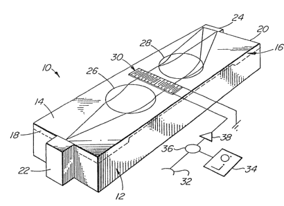
With reference to FI~UR~ 1, there is illustrated an
integrated optical spectrum analyzer 10, compri~ing a
~ubstrate 12, ~ormed of Lithium Niobate (LiNbO~), having
a sur~ace 14 in which the waveguide 16 of .the pre~ent
invention i5 formed. The waveguide i5 formed with an
input edge 18 at one end of the ~ub~trate and an output
edge 20 at the other end of the substrate remote from
. A ,.
and opposed tQ the first edge. A light ~ource 22, ~uch
a~ a laser diode, is coupled to the input edge in l~ght
transmitting relation thereto while a detector means 24
is coupled to the output edge in light transmitting
r lation thereto both ln well known fashion. The
wavegulde further includes a collimating lens 26 and a
Fourier lens 28 longitudinally spaced from the
collimating len3 tnwarAs the output ed~e. A surface
activated wave (SAW~ mean~ 30 i8 secured to the
waveguide, in transverse relatlon thereto, between the
collimating and Fourier lenses in well known fashion.
As is also well known, an electrical signal to be
analyzed i5 input at 32 and mixed with the output of a
local o~cillator 34 in a mixer 36. The resulting signal
ls amplified by an amplifier 38 and applied to SAW means
30 which directs the signal txansversely of the
longitudinal or optical axis of the waveguide.
With particularly reference to ~I~URE 2 of the
drawings, waveguide 16 will be seen to include an input
out-diffused waveguide section 40 extending from input
edge 18 toward~ output edge 20, an output out-diffu~ed
waveguide section 42 extending from output. edge ~0
towards input edge 18, and a titanium in-diffu~ed SAW
propagation waveguide section 44 extendin~ transver~ely
of the ~ubstrate and intima~ely connec~ed to eaah of the
input and output waveguide sections by means of narrow
transition regions 46 and 48. Collimating lens 26 and
Four1er lens 28 are disposed in the in-diffused
waveguide section 40. The depth of each out-di~fu~ed
s~ction is madQ greater than the d~pth of said
in-diffused ~ection by about one order oP magnituda.
, ....
i4~
g
It will be understood by tho~e s~illed in the art
that while the transitlon region~ are descr~bed a~ being
narrow, the width, along the longitudinal or optical
a~is ~f ~aid waveguide, of the transition regions must
be much greater than the wavelength of the optical
~ignal pa~sed throu~h the wave~uide in order to avoid
reflection oP the si~nal in the traneition regions.
The above described waveguide structure po~es~e~
several favourable attributes. It can decrea~e the
level of in-plane scattering cau~ed by surface
irregularities in both planar and non-planar surfaces,
reduce th~ dif~iculty o~ coupling light into and out o~
the waveguide, ~unction as a TM mode ~ilter, and
increase the inten~ity of light ~ocussed in-to the gulde
beyond the li~its imposed by the optical damage
r~sistance o~ a strictly in-dif~used waveguide. In
addition, no visible scattering occurs at the transition
region. These attributes may be explained in part by
the i~dividual characteristic~ of the out-diffused and
in-diffu~ed waveguide section~.
A low loss out-di~fu~ed wav~guide i9 created by
heating a LiNbO3 crystal -for a period ran~ing from a few
minutes to several hour~ at a temperature near lOOO~C
(but less than the Curie temperature of the crystal3.
Heatin~ the cry~tal causes the Lithium to diffu~e out
and evaporate away leaving a re~ion at the Rurface which
exhibit~ an extraordinary refractive index of refraction
sllghtly higher in value than the bulk crystal index of
refraction. The increa~e in the index allows only T~
polarized modes to propagate ~ince the ordinary
rePractive index of the crystal remains unaffected by
the dlf fusion proce~s.
, ....
~6~7
--10--
Th~!? rasulting waveguide penetrates the cry~tal
~;ub~trate much further than in-dlffused guides:
extending 10 or 20 ~m or more into the sur~ace of the
crystal. Con~equently, most of the energy in the
propagating modes lies further from the surface o~ the
crystal than the energy in the in-diffused waveguide
modc~.
The out-diffused waveguide i~ also inherently more
r~sistant to optical damage than in-diffused guides for
reasons that are not completely understood.
These characteristic~ may be exploited in the
several way~. Because of the ~eeper mode penetration,
the modes are le~s susceptible to surface imperfections
and hence the level of in-plane sca~terin~ is reduced.
Further, no surface polishing is required to remove
diffusion ~y-product~ which may appear in the
in-diff U5 ion process.
The deeper waveguides also decreases the coupling
difficulty since the physical constraints imposed by
couplin~ to a 20 ~m thick waveguide are ~ar less
string0nt than those imposed by a 2 ~m thick wave~uide.
This is a qi~ni~icant advanta~e when direct
butt-coupling is used ~or input and output coupllng.
The relatively large waveyuide thickne~s alleviates the
a~ial and trar~verse la~er diode positioning
di~icultie~ as well as provides a low diver~ence beam
when light exits the waveguide. Furthermore, coupliny
to optical ~lbers could be improved since the fiber core
diameter and planar waveguide thicknes~ are more closely
matched in size. The inability of out-diffused
waveguldeq to carry TM modes allows the wav~guide
struc~ure to act aæ a mode ~ilter ~or beams pas~ing from
.
the in-diffu~ed waveguide 3ection to the out-di~fused
wavegulde ~ection.
Notwith~tanding the aforedescribed advantages,
out-dif~used waveguides are not suitable media for
acousto-opti~ Bragg interaction because the deep optical
mode penetration offers a poor overlap with hi~h
frequency surface acoustic waves. The poor overlap
results in inefficient Bragg deflection at frequencies
nearing 1 GHz and beyond. On the other hand,
in-diffu~ed waveguides are ideally suited to this
~unction but suffer from the disadvantages ~entioned
earlier. Accordingly, the waveguide structure of the
present invention Gombines both types of guides and
provides the option of placing the type of waveguide on
the crystal where it is the most advantageou~ to the
d~vice as a whole. For example, as described earlier
with respect to an ~OSA, the edge~ employ out-diffu~ed
waveguides whereas the SAW propagation section and
~eodesic lenses employ an in-diffused guide.
The fabrication of the waveguide of the pr~sent
invention is simple, straightforward and readily
reproducibl~. A non-contact mask is used to deposit a
layer of titanium on one side of the cry~tal with a
gradcd thickne~s transltion re~ion of approximately 1 mm
in width. The cryetal i~ then placed in a tube ~urnace
where it is heated to 1000C whlle argon gas i8 bubbled
through water and pas~ed through the furnace for a
suitable time interval, including the heating up period
and up to the first few hours of the diffusion period,
at 1000C. Titanium ln-diffusion is well known in the
art and, accordingly, the details thereof are not
described in detail herein. This forms the in-dif~used
,
-.12-
waveguide on the titanium covered ~idc o~ thc crystal
while preventing any out-dl~fu6ed region from forming
elsewhere.
In th~ next step, the wa~er bu~bler is by-passed
and only dry argon is used during a time interval, which
may ran~e from several minutes to several hours
depending upon the des~red depth o~ the out-diffu~ed
s~ction, ~o that the out-diffused waveguide can be made
on the part of the crystal ~urface which was not covered
inltially with the titaniu~ ~ilm. Following this, the
argon is replaced by oxygen and the crystal i8 permitted
to cool to room temperature. This procedur~ results in
clear waveguides with no visible transition regions.