Note: Descriptions are shown in the official language in which they were submitted.
~z~
SPECIFICATION
Backqround of the Invention
The present invention relates generally to loss
of voltage detectors, and in particular to circuitry for
detecting and indicatin~ the loss of voltage in a power
di&tribution ~ystem.
It is often neces6ary in comanercial electrical
di~tribution ~y~tem~ to provide an alarm and/oÆ control
function in the event of a power interruptio~. For example,
it may be required that electrical power generating
equipment be started in the event of a power failure to
maintain critical e~uipment in operation, or that certain
types of electrical equipment be disconnected from power
mains in the event of a power failure to prevent damage upon
restoration of power. Furthermore, in the case of
multi-phase power ~ystems, it may be required that certain
equipmen~ be di~connected following a failure in one phase
in order ko avoid potentially damaging ~ingle-phase
~peration of the equipment. Loss of voltage detector~,
particu~arly those adapted for use with commercial power
distribution sy~tems, are useful for automatically
implementing such procedures in the even~ of power failure.
In the case of high voltage power mains, high
impedance coupl ing of the loss of voltage detector to the
25 power mains is de~irable in order to provide isolation from
'che high vol~age~ present in the mains. The }085 of voltage
"~
detector of the pre~ent invention utilizes such preferred
high impedance coupling for both energization of its
circuitry and for providing an external control effect.
Consequently, coupling to high voltage conductors can be
readily accompli~hed at such conventional locations as high
impedance underground cable termination te~t point~.
The loss of voltage detector of the present
invention constitutes an imprsvement over the detector .
described in U.S. Patent No. 4,550,288 of the present
inventor, in that it provides a higher impedance input,
facilitating its use high impedance test points and on high
voltage overhead lines, and a faster recharge time,
facilitating the detection of recurring voltage
interruptions. Like the detector described in U.S. Patent
No. 4,550,288~ the detector of the present inventîon
provide~ a control effect in the form of closure of a ~et of
relay contacts, which can easily be adapted to actuate other
electrical system~ and equipment, a~ described in ~he
patent.
Accordingly, it i~ a general object of the present
invention to provide a new and improved loss of voltage
detector.
It is another object of thi~ invention to provide
a 10~6 of voltage detector having a high impedance input
suitable for use in conjunction with high impedance test
points and high vol~age electrical power line~.
It i~ another object of this invention to provide
-- 2 --
~L~6~
a new and improved loss of voltage voltage detector which is
energized and triggered by means of high impedance coupling
to a hi~3h voltage power line.
Sumlnary of the. Invention
A loss of voltage detector for proclucing a control
effect in response to the loss of voltage in a monitored
conductor includes a fi~t capacitor, a ~econd capacitor,
and charge circuit mean~ powered by alternating current in
the conductor for developiny a charging current for char~ing
the first and second capacitors. Voltage limiting means
connected across the second capacitor limit the ~oltage
developed across that capacitor during charging. Charge
transfer circuit means operable upon interruption of the
charginq current transfer a portion of the charge on the
first capacitor to the ~econd capacitorg causing the
terminal voltage across the second capacitor to reverse
polarity and progressively increa e in the reverse direction
a6 the charge i~ transferred. Trigger circuit means
responsive to the voltage acro~s the second capacitor
increasing beyond a predetermined threshold level discharge
the firs~ capaci~sr through an indicating device to pro,7ide
a control effect followi~g loss of voltage in the
cond~ctor~
Brief Description of the Drawings
The features of the present invention which are
believed to be novel are ~et forth with particularity in the
appended claim6. The invention, together with the further
obje~t~ and advantages thereof~ can best be understood by
reference to the following description taken in conjunction
with the accompanying drawings, in the several figures of
which like reference numerals identify like elements, and in
which:
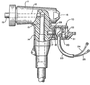
Figure 1 is a ~ide elevational view, partially in
~ection, of a loss of volta~e detector constructed in
accordance with the in~entiGn installed on the test point
terminal of a conventional elbow connector of the type
commonly used in power distribution systems.
Figure 2 is an electrical fichematic diagram of the
10SB of voltage detector shown in Figure 1.
Figure 3 i6 a perspective view of an alternate
embodiment of the 10~6 of voltage detector of the invention
installed on an overhead power line~
Figure 4 i8 a cros~-sectional view of the
alternate con~truction taken along line 4-4 of Figure 3.
Figure 5 i6 a cro~s-sectional view taken alony
line 5-5 of Figure 4.
20Figure 6 is a cross-sectional view taken along
line 6-6 of Figure 5.
Figure 7 is an elec~rical ~chema~ic diagram of the
loss of voltage detector shown in Figure 3.
~igure~ 8-10 are a series of views illustrating
the functioning of the indicator flag assembly utilized in
the 108~ of voltage detector of F~gure 4
Description of the Preferred Embodiment
~2~
Referring to the drawings, and particularly to
Figure 1, a loss of ~oltage detector lû constructed in
accordance with the invention is shown in conjunction with a
conventional plug-in el~ow connector 11 of the type commonly
5 used in high voltage alternating current sy~tems for
establishing plug-in connections to transformers or other
devices (not shown). As ~hvwn, the connector 11 includes
generally an axial conductor 12, an insulating jacket 13,
and an electrically-conductive outer sheath 14, the sheat~
being grounded in accordance with conventional practice. A
plug-in contact 15 extends from conductor 12 and is arranged
to connect with a comple~entary contact on the transformer
or device to which the c.onnector i6 connected. A hancllinq
loop 16 having e nds anchor ed i n the co nductive sheath
lS extends from the connector to receive the hooked end of a
lineman' s tool to facilitate installation and removal of the
connector~
In accordance with conventional practice, elbow
connector ll includes along one ~ide a radially-projecting
test point 17 which includes an exposed contact 18
capaciti~ely coupled to conductor 12. In operation, loss of
voltage detector 10 is mounted on this test point~ as
illustrated in Figure 1.
Los~ of voltage detector lû includes a hollow
rubber outer shell 20 which i5 open and dimensioned at one
end to engage test poi~t 17. Electrical component~ of the
detector are mounted on a disc-shaped circuit board 22
-- 5 --
~ ~6 ~
within a cylindrical housing 21 contained within the outer
shell.
In order to interconnect the loss of voltage
detector 10 with other equipment, such as an alarm or
control sy~tem, the detector includes an electrical cable 23
which extends through an aperture in the bottom of shell 200
A pair of conductors 24 and 25 within the cable connect at
one end to circuitry on circuit board 22, and at their other
end to the equipment to be controlled (not shown).
Circuit board 22 is preferably mounted perpen-
dicular to the axis of housing 21 in a location intermediate
the ends thereof, and may be secured in position by a layer
of epoxy within the housing. An electrical connection is
established between the circuitry of the detector and test
15 point contact 18 by means of a helical ~pring 29, which is
anchored to the ci rcuit board at one end and bia6ed against
contact 18 at its other endO Contact 18 i~ rigidly mounted
within the insulating material 13 of connector 11 EO that
the di~tal end of the contact i8 in proximity to conductor
12. This establishes capacitive coupling bet,ween the
conductor and the contact, thereby providing operating power
and loss of voltage sensing capability to the detector. A
feature of the lo~ of voltage detector of the present
invention i~ that ~atisfactory operation can be achieved
with a capacitive coupling between contact 18 and conductor
12 a~ low a~ 5 picofaradsO
Referring to Figure 2, the loss of voltage
~ILZ~4~9
detector circuit includes circuit mean~ for producing a
pulsatîng unidirectional charging c~rrent in response to
alternating voltage present on test point 1~., In
particular, thi~ circuit means include a briclge rectifier
network 30 compri~ing four rectifier diodes 31~34. One
input terminal of network 30, formed at the juncture of the
anode of diode 31 and the cathode of diode 32~ is
electrically connected throu~h helical ~pring 29 to test
point contact 18. The other input terminal of the rectifier
network, formed at the juncture of the cathode of diode 33
and the anode of diode 34, is connected to ground through
the conductive sheath 14 of the elbow connector. The
positive polarity output terminal of the bridge rectifier
network i6 formed at the juncture of the cathodes of diodes
31 and 34, and the negative polarity output terminal is
formed at the juncture of the anodes oP diodes 32 and 33
The pul~ating unidirectional chargin~ current
developed at ~he output terminals of bridge rectifier
network 30 i~ applied to fir~t and ~econd capacitor~ 35 and
~0 36, which are connected in series-circuit relationship
acro~s the positive and negative polarity output terminals
of the network. This causes the capacitors to be charged in
the presence of an alternating voltage on conductor 12. A
foward-biased diode 37 i~ connected across capacitor 36 to
25 limit the voltage developed across this capacitor during
charging to the forward voltage drop of the diode, typically
in ~he order of 0~7 volts. Capacitor 35 i6 con~equen ly
charged to the difference between this voltage drop and the
output of the rectifie{ network, which may be limited by a
zener diode 39 to approximately ~ volt~
To provide for a portion of the reiati~ely greater
charge on capacitor 35 to be transferred to capacitor 36 in
the absence of a charging current from recti~Eier netw~rk 30,
a re i~tor 38 i5 connected acros6 the ~eries co~bination Df
capacitors 35 and 36. Upon loss of output from rectifier
network 30, the r~latively greater voltage level acros~
capacitor 35 causes current flow from thi~ capacitor throuyh
resistor 3B to capacitor 36. This results in a sudden
rever~al in polarity and a progressively increasing voltage
in the reverse direction across capacitor 36.
To ~ignal the occurrence of the increasing rever~e
polarity ~oltage acros~ capacitor 36, an enhanced FET-type
transi~tor 40 i8 provided with control electrode~ connected
acro~s the capacitor. In particular, one principal
electrode of the transistor is connected directly to the
co~mon terminal~ of capacitors 35 and 36, and the gate
20 elec~rode of the transistor i8 connected through a resistor
41 ~o the remaining non-common terminal of capacitor 36.
The remaining principal electrode of the transi~tor is
connected through the magnetic winding of indicator means in
the form of a relay 42 to the remaining non-common terminal
2S of capacitor 35. A ~et of normally open contact~ 43
associated with the relay are connected by conductors 24 and
25 to an external device to be controlled.
~Z1~ 9
In operation, with AC voltage present on conductor
12, the unidirectional current pulses produced by bridge
rectifier network 30 are applied to capacitors 35 and 36,
causing capacitor 36 to be charged to the fo:cward-bias
5 voltage drop of diode 37, and capacitor 35 to be charged to
the output voltage level of network 30, less the forward
drop of diode 37. In a 60 hertz system, the unidirectional
current pulses are produced by network 30 at a rate of 120
hertz, and the discharge time constant of the capacitor
circuit, determined primarily by the capacitances of the
capacitors and resistor 38, i5 sufficiently long so that the
capacitors remain ~ubstantially fully charged to their
respective terminal voltages between charge current
pul~es.
In the event of a power failure in conduc~or 12,
the output of bridge rectifie~ network 30 drops to zero,
whereupon a portion of the relati~ely greater charge in
capacitor 35 i~ transferred through resi~tor 38 into the
relatively lesser charged capacitor ~6. Since diode 37 is
20 reverse-biased to this current flow, the diode has no effect
on the charge transfer, Relative to the common connection
between capacitors 35 and 36, capacitor 36 experiences a
change in polarity and a progre~sively increasing terminal
voltage a~ the charge transfer progresses. The rate of
25 charge transfer i8 dependent on the time constant provided
by the serie~ combination of capacitors 35 and 3~ and
resistor 38, and in practice is selected to avoid triggering
~;~64~
of the detector in respon~e to transient~, while providing a
~ufficiently fast re~ponse to actual voltage los~es to avoid
damage to controlled equipment. ~urthermore; the capaci-
tance of capacitor 36 is preferably ~ubstantially les~ than
that of capacitor 35 ~o that only a ~mall portion of the
accumulated charge on capacitor 35 i~ transferred to
capacitor 360 In practice, a capacitance ratio of 100-to-1
or greater may be provided between the two capacitor~.
The progres~ively increa~ing ~oltage acro~
10 capacitor 36 is applied to the gate electrode and one main
electrode of transistor 40 through resi~tor 41. When the
applied voltage has rever~ed polarity ~o a~ to forward bias
the transi~tor, and has reached the threshold level of the
transi~tor, typically 3.5 volt~, the transi~tor becomes
conductive and capacitor 35 i8 di~charged through the
winding of relay 42, closing contact~ 43 and providing a
control e~fect to an external device.
Contact~ 43 remain closed until capacitor 35 ha~
di~charged to a level where insuff icient current exist~ to
continue to actuate the relay, after which ~he contact~
open. Since no out~ut i~ being developed by bridge
rectifier network 30 at this time, capacitors 35 and 36 are
not recharged and no further control effect i8 developed.
~owever, upon re~toration of voltaye in conductor 12 the
25 Gapacitor~ are again charged and the voltage rever~al acros~
capacitor 36 again conditions transi~tor 40 to cut-of0
In a typical embodiment intended or use with 60
-- 10 -- `
~264 51~9
hert~ alternating current power distribution system~,
capacitor 35 may have a value of 1 microfarad and capacitor
36 may have a value of .01 microfarad. Resi~tor 38 may have
a value of 50 megohm6 and 2ener diode 39 may have a
5 threshold voltage of 50 volts. The~e component values
re6ult in capacitor 35 havin~ a discharge time constant o~
approximately 0.1 second7 allowing the voltage lo~ detector
to remain insen~itive to momemtary vol~age losses of 6hort
duration, such as those which may occur during 6witchin~
operations. Diode 37 may comprise a type lN4007, transistor
40 may comprise a type IRFD lZ3 enhanced FET, and resistor
41 may have a value of approximately 50 megohms to provide
i~olation between capacitor 36 and the transistvr~
An alternate embodiment of the invention ~uitable
15 fsr mounting directly to a high voltage cable of a power
distribution ~y~tem is ~hown in Figures 3-7~ As shown, this
loss of voltage detector 60 includes a generally cylindrical
housing 61 formed of a hard electrically insulating
weather-re6istanS material such as LEXAN ta trademark of
General Electric Company, Schenectady, New York). The
detector 60 i8 secured to a conventional high voltage cable
62 including an internal conductor 12 by mean~ of a pair of
resilient inwardly-bia~ed non-electrically conductive
retaining arms 63 and 64. The retaining arms, which project
rearwardly from housing 61 ? include end portions 63a and
S4a, respectively, which are inwardly formed so as to grasp
and hold cable 62 in close proximity to the rear wall 65
-- 11 --
~648Q~
~Figure 4) of housing 61. A pair of ~emi-resilient
stiÇfening member~ 66 and 67 may be provided in close
a~sociation with member~ 63 and 64 to as~ist in biasiag ~he
~etain~ng member against cable 62~
As shown to bes advantage in Figure 4, upon
inser~cion of cable 62 between the retaining member~, the
ends of the retaining members are forced apart as shown.
Thi~ allows housing 61 to be pushed up against the cabl~,
and as the cable abut~ the housing the end portions of the
retaining members push the cable into engagement. This
.
cable attachment arrangeme~t is described and claimed in
the copending ~pplication of the preserlt inven~or~ enti~led
~Cable Moun'ced Capacitively-Coupl~d Electrical Indica~ing
DeYice"~ U.S. Patent No. 4,794,329, issued December ?7, 1988.
~o provide an indication of voltage loss, detector
60 in~lude~ on the front wall 68 o~ housing 61 a window 70
1:hrough which an indica~or ~lag agsembly 71 proviae~ a
visible indication following voltage 10~:8. A handling loop
72 having end~ anchored in the front wall extends ~rom
housing 61 to receive the hooked end of a lineman' ~ tool to
facilitate installation and removal of the indicator from
cable 62.
~he various circuit components of the ~os~ of
2~ voltage de~ector are mounted on a circu~t board 73 contained
within housing 61. Electro6ta'cic coupllng between the high
impedance detector clrcuitry and a fir~t pick-up point in
:~2~ 9
the electric f ield ~urrounding conduc'cor 12 is provided by a
flat electrically conductive plate 74 positioned within
housing 61 near rear wall 65 and electrically connected S~o
the circuitry by a conductor 75. Electrostatic coupling to
5 a second pick-up point radially ~paced from the first
pick-up point relative to conductor 12 i~ provided b~ an
electrically canductive ring 79 and an underlying
electrically conductive coating on the inside surf ace of
housing 61 adj~cent and behind front wall 68. Thi~ housing
10 construction, which advantageously provides sufficient
ex~ltation to the circuitry without the use o~ external
ground plane elements, is described in detail in the
aforementioned u.s. Patent No. 4,794,329.
of the pr esent inventor .
Referring to Figure 70 the circuitry of loss of
voltage indicator 60 may be basically identi~al o that of
indicator 10. Specifically, pic~up ~late 74 is connected by
conductor 75 to one input terminal of a bridge rectifier
ne~work 80 comprisillg rectif ier diodes 81-84 . Th~ other
20 input terminal of rectif ier network 80 i8 connected to ring
79. With this arrangement, in the presence of a high
voltage alternating curren on conductor 12 the potential
difference provided by plate 40 and by ring 79 i~ impressed
across the input terminals of the rectifier network. The
2$ network rectifies this current to develop a pulsating
charging current which is applled to capacitor~ 85 and 86,
which are connected in ~erles across the network outpu~
13
~'~6~8~'~
terminal~. A forward-biased diode 87 limit the voltage
developed across capacitor 86 by the changing current and a
zener diode 88 connected across the netw~rk limit~ the
voltage developed by the network.
Upon loss of excitation a portion of the chaxge on
capacitor 85 i~ transferred through resistor 8g to capacitor
86, causing the voltage across that device to reverse
polarity, and to progre~sively incr ase in the reverse
direction as the capacitor is charged. When thi6 increa6ing
voltage of reverse polarity reaches the conduction threshold
voltage level of an enhanced FET-type transistor 90 having
control electrodes connected to the capacitor through a
re~istor 91, the transistor become~ conductive and cause6
capacitor 85 to discharge through a magnetic winding 92 of
indicator flag assembly 71. This cau~es the repo~itioninq
of a member flag contained in the assembly which, when seen
through window 70, alerts an observer that a 1058 of voltage
ha~ occurred in conductor 12.
The con~truction and operation of the indicator
fla~ assembly 71 is illustrated in Figure~ 8-10. ~he
indicator assembly, which i8 located at the forward end of
housing 61, i seen to comprise a disc-shaped flag member
95, a shaft 96, a flag actuator magnet 97, and a generally
U-shaped pole piece 100. ~he 1ag member include~ red and
white indicator seyment~ 95a and 95b on oppo~ite ~ide~ of
the axi~ of rotation~ When the fla~ member i~ aligned in
the reset po6ition ~hown in Figure~ 8a and 8b only the white
6~8~
indicator segment 95b is visible to the observer through
window 70, indicating a reset condition. ~owever, upon
~cc~rrence of a fault condition, the flag member rotates
180 such that the red indicator segment 9~a i~ vi6ible
through the window indicating that a los~ of voltage ha~
occurred.
Actuation of flag member 95 between the reset and
fault indicating position6 is ac~omplished by actuator
magnet 97, which i8 rotatably coupled to the flag member by
10 shaft 96~ The shaft is maintained in alignment with the
axis of housing ~1 by means of a bearing surface in an
interior divider wall 98, located behind the front wall 68,
and a bearing surface in the f ront wall.
The actuator magnet 97, which may be formed of a
magnetic material havinq a high coerci~e ~orce, ~uch as ~
ceramict is forme~ to provide a pair of diagonally opposed
magnetic poles of opposite polarity. The actuator magnet,
and hence the indicator flag, are normally biased to the
reset-indicating position 6hown in Figure6 8a-8b by means of
magnetic pole piece 100, which is formed of a magnetic
material having a relatively low coercive force, ~uch a~
chro~e steel, and which includes two magnetic pole6 of the
magnetic polarities shown in Figure6 8a-8b in magnetic
communication with the actuator magnet.
Vpon 106s of voltage in conductor 12, pole piece
100 and an adjacent auxiliary pole piece 101 are
remagnetized to the magnetic polaritie~ ~hown in ~igure~
- 15 -
9a-9b and lOa-lOb by the di~charge of capacitor 85 through
magnetic winding 92, which is located on the pole piece, as
shown. As a result, the poles of flag a tua~or ~agnet 97
~re repelled by adjacent like-polarity poles of the pole
5 pieces and the indicator flag i~ caused to rotate 180 to
the indicating position shown in Figure~ lOa lOb. In this
position, the red indicator segment 9Sa of the indicator
flag is visible through window 70 and a li.neman viewing the
los~ of voltage indicator is advised that a voltage loss has
occurred in conductor 12.
The indicator fla~ remains in the loss of voltage
indicating pos.ition until pole pieces 100 amd 101 are
subsequently remagnetized to the magnetic polarities shown
in Figures 8a-8b by momentary application of a remagnetizing
force from external means. In particular, ~uch
remagnetizing force may be provided by a permanent magnet
held in close proximity to the front wall 68 of lcss of
voltage indicator ~0, the desired remagnetizing effect being
confirmed by a sim~ltaneous repositioning of flag indicator
20 95 to a reset-indicating position as viewed through window
70.
A magnetic shield 105 comprising a flat plate of
magnetically conductive material i6 provided between the
actuator assembly and conductor 12 to shield the a~tuator
25 assembly from the magnet field which accompanies occurrence
of a fault current in conductor 120
While the indicator flag as&embly 71 has been shown
- 16 -
in conjunction with the cable-suspended loss of voltage
indicator of Figures 3-7, it will be appreciated that the
indicator assembly can al~o be provided in the test point
mounted indicator of Figure 1. In this caset the indicator
flag mechani6m would be preferably dimensione~d to fit within
the indicator housing 21, and magnetic winding 92 would be
connected in place of relay winding 42.
By reason of the high input impedance provided by
the los~ of voltage indicating circuit, sufficient
excitation is obtained in test point-mounted and
cable-mounted environments for operation of the indicator
without the need for external grounding connection~ or
electrically conductive members projecting from the housing.
Thi~ result~ in a compact and efficient 10ss of voltaye
indicator completely free of external appendages which might
produce corona or present a shock hazzard.
While particular embodiment~ of the invention
have been shown and described, it will be obvious to those
~killed in the art that change6 and modification~ may be
20 made therein without departing f rom the invention in its
~roader aspect6, and, therefore, the aim in the appended
claims is to cover all such changes and modif ications as
fall within the true spirit and scope of the invention.
- 17 -