Note: Descriptions are shown in the official language in which they were submitted.
A DIGITAL TELEPHONE SWITCHING SYSTEM H~ING A MESSAGE
SWITCH WITH ADDRESS TRANSLATION
The invention relates general:Ly to a digital
telephone switching system and more particularly to such a
system having a message switch that provides address
translation.
The contemporary telephone switching system is a
common control stored-program machine usually comprising a
central processing unit, a switching network and a plurality
o~ peripheral units for connecting to subscriber lines,
trunks or digital carrier facilities. The central processing
unit communicates with the peripheral units through the
switching network via a central message controller. The
processor receives operational requests and responds thereto
with commands to the various functional units oE the system.
A complete description of such a system is available from
United States patent number 4,213,20~ issued July 15, 1980 to
the same assignee as that of the present application. The
main hardware modules of that system are the central control
unit (CC), the central message controller (CMC), the input-
output controller (IOC), the switching network (NM~, and the
peripheral modules (PM).
The core equipment (CC, CMC, IOC, and NM) is
continuously being evolved mainly to increase system capacity
and remove capacity bottlenecks in network traffic handling,
system control messaging, and real time processing of calls.
In a recent architectural evolution of the system, the
control message multiplexing function of the CMC (one CC to
many network/peripheral modules) was replaced by the message
distribution function of a new system element, the message
switch (MS). The message switch is a high capacity frame
switch which can route messages between any and all of its
ports. It operates as a high-bandwidth local area network,
interconnecting various system processors. Thus, multiple
control processors can share access to multiple
network/peripheral modules via the message switch. In
addition, autonomous messaging between network/peripheral
modules can occur~ The message switch provides a greatly
~,~
3L264~4L5
increased message bandwidth over the CMC.
In conjunction with the introduction o-f the
message switch, a new computing module (CM) was developed to
replace the CC and thus provide increased processing power.
To provide communications between the MS and CM a shor~ range
fiber optic transmission link operating at high bit rates is
used. Its full bandwidth is available for CM message
transmission, thus ensuring that transmission links are not a
control message bottleneck in the system.
Since the message switch is configured as a LAN,
its funetion consists in transferring a message from one of
its ports to another one of its ports under control of its
microprocessor. Thus, the MS is the messaging hub of the
system, allowing various subsystems connected directly
(computing module, switching network, I/O controller) or
indireetly (peripherals) to it~ ports, to eommunieate freely
with each other.
The m~ssage switeh eomprises a proeessor (MSP), a
transaction-bus (T-bus) for performing port-to-port
switchin~, a processor bus (P-bus) for interconnecting the
MSP with other elements of the MS and data port cards for
eommunieation between the MS and the remainder of the system.
The transfer of messages through the MS is done over the T-
bus which performs basieally as a packet switch. Each
message to be routed contains a header comprising a
destination address eoxresponding to an outgoing port o:E the
switch. Eaeh port is adapted to recognize is own address and
thus aceept messages on the bus. Therefore, in a message
transfer/ the destination for a data ~r message transfer is
identified during an address eyele that precedes the data
transfer.
In this type of system which has large portions
thereof duplicated for reliability and which operates as a
distributed processor it has been found desirable to define
the destination of some messages by the function of its
reeipient and not by its physical appearance on a port of the
message switch. Thus, whenever data links from the MS to
functional units are reconfigured for whatever reason such as
~264 514~
failure, maintenance, evolution of the system, or other, the
functional destination remains the same.
Therefore, in accordance with the invention, the
message switch is provided with a mapper circuit. ~ach
message header is provided with a phys:ical address and a
logical address and the mapper circuit is responsive to a
predetermined physical address for translating the logical
address to a physical address and for replacing the
predetermined physical address with the translated physical
address.
A further advantage of having a mapper circuit in
the message switch is that it provides the capability to flag
various logical addresses for monitoring purposes and allows
multiple logical addresses to be mapped to the same physical
address.
An example embodiment of the invention will IIOW be
described in conjunction with the drawings in which:
Figure l is a block diagram illustrating the
architecture of a prior art telephone switching system;
Figure 2 is a block diagram illustrating the
architecture of a digital telephone system having a
distributed control structure and a message switch with
address translation in accordance with the invention;
Figure 3 is a block diagram of the message switch
of figure 2;
Figure 4 is a diagram of the message format used
in the message switch of figure 3;
Figure 5 is a block diagram of the mapper circuit
of figure 3;
Figure 6 shows the configuration of the data
tables in the memory illustrated in figure 5; and
Figure 7 is a flow chart illustrating the
operation of the control state machine shown in figure 5.
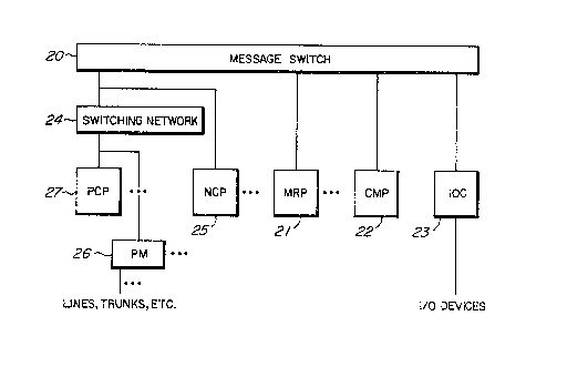
Figure 1 illustrates the control structure of a
contemporary digital telephone switching system which
comprises a central control unit (CC) 10 connected to
input/output devices via a central message controller (CMC)
11 and an input/output controller (IOC) 12. The central
i4~
control unit 10 is also connected to lines and trunks of the
telephone network via the CMC 11, a switching network (NM) 13
and peripheral modules (PM) 15, the latter being controlled
by peripheral control processors (PCP) 14. Although some or
all of the blocks or modules of such a system comprise a
respective microprocessor, the call process control resides
enti.rely in the central control 10 of the system. That is,
the CC 10 receives info.rmation from the other units of the
system and responds appropriately with commands and
instructions to perform the usual functions of a switching
office such as call routing and maintenance procedures.
In order to unload the central processor and thus
increase the call handling capability of the system, it is
desirable to replace the central message controller 11 which
simply routed calls from and to the CC 10 with a device that
allows the various subsystems connected directly or
indirectly to its ports to communicate freely with each
other.
Figure 2 shows the architecture of a telephone
system having a distributed control structure and comprising
a message switch 20 which is the messaging hub of the system.
Its data ports are shown connected to various functional
units of the system such as the message routing processor 21,
the call management processor 22, and the input/output
controller 23. It is also connected to the switching network
24 controlled by the network control processor 25 and to the
peripheral modules 26 controlled by the peripheral control
processor 27 via the switching network 24. Since the message
switch is basically a high capacity frame switch, any pair of
the units or nodes connected to it may exchange messages
autonomouslyO Each unit wishing to send a message to another
unit assembles the message as a packet of data preceded by
the address of the destination and each message received at
the message switch is routed in accordance with the
destination address.
Figure 3 is a block diagram showing a message
switch 30 comprising a message switch processor (MSP) 31, a
clock circuit 32, a mapper circuit 33 as well as a processor
6igl8~
bus (P-bus) and a transaction bus (T-bus). The switch 30 is
connected to the functional units of the switching system
(fig.2) via port cards 34 which are adapted to receive data
messages in accordance with any one predetermined protocol
such as DS-30, DMS-X, DMS-Y, HDLC, DS-512. These protocols
are discussed in various publications including United States
patents number 4,698,809 and 4,750,165.
Each port card handles bidirectional data streams
and includes input and output buffers for storing the data
messages in transit. The port cards 34 are connected to the
T-bus of the message switch and each one is adapted to
recognize its own address on the bus. Therefore, each data
link channel to the functional units is addressable by
specifying the card and channel address identification of the
destination node. A port card contains multiple ports (e.g.
32) which are referred to as channels. They may indeed be
channels in a time division multiplex data link or they may
be separate physical links. ~lthough not shown, the port
cards, are also connected to the P-bus for configuration
control and maintenance.
From a functional point of view, the T-bus
consists of an address/data bus which comprises a 32-bit
wide, bidirectional bus carrying multiplexed address and data
information, a control/status bus identifying the various
states of the address/data bus, such as address cycles, data
cycles, end-of-message cycle, etc..., an access control bus
for implementing an arbitration scheme for resolving bus
contention, and a timing bus carrying all the necessary clock
signals for the operation of the bus and the port cards.
As will be discussed later, the mapper circuit
includes address translation tables. The MSP 31, clock
circuit 32 and mapper circuit 33 communicate over the P-bus
which controls the functions of the message switch~ The MSP
is allowed to communicate with other ports of the MS via a T-
bus appearance through interface circuit 35. The translation
tables of the mapper circuit 33 may be updated via the P-bus.
4~
As discussed previously, it is desirable in many
cases to identify the destination address of a message by its
logical or functional address. Therefore, the message switch
must be able to support two types of addressing modes as
shown in the message header field of the message format
illustrated in fiyure 4. The physical address of a message
destination is identified by thP port card and data channel
on that port card. The logical address of a message
destination corresponds to a destination node identification.
These two addressing modes are referred to as mapper bypass
and mapper assist respectively. The source of the message
indicates explicitly which mode is to be used by the message
switch by using one predetermined physical address in the
header, for example all ONE bits, which is recognized by the
mapper circuit only. The latter is then responsive to its
predetermined physical address to translate the logical
address contained in the header of the message to a physical
address on the T-bus. This is done without the mapper
circuit 33 receiving the body of the messa~e; it manipulates
only the message header.
Figure 5 is a blocX schematic diagram of the
mapper circuit 33. It comprises a mapping memory 40
controlled by a state machine circuit 41. Locations of the
memory 40 are selected by an address select circuit 42 which
is connected directly to the P-bus, and is connected to the
T-bus via a logical address register 43. The address select
circuit 42 is also connected to a refresh circuit 44 adapted
to refresh the content of the memory 40. The data port of
the memory 40 is connected directly to the P-bus and to the
T-bus via a physical address register 45. The mapping memory
40 thus receives: 1) T-bus logical addresses to be mapped to
corresponding physical addresses, 2) translated physical
addresses to be checked for validity, 3) refresh addresses,
and 4) P-bus addresses from the MSP 31. In this embodiment,
the memory 40 is a dynamic RAM, which therefore requires a
periodic refresh. This may be done using a staggered refresh
in which successive locations are refreshed at a rate such
that the time to refresh them all is equal to the refresh
7 ~2~
rate. Of course, a static RAM which does not require refresh
may also be used.
A mapping or translation operation consists of
three to five separate phases which are initiated when a
mapper-assist request is received on the T--bus: that is, when
the mapper circuit 33 detects its predetermined address (e.g.
all 'ls') in the physical address portion of the header in a
message. This operation presents the memory with the first
two of the four addresses referred to above.
The mapping memory 40 contains several data tables
which hold th~ data used to per~orm map operations for the T-
bus. These tables are shown in figure 6. Two of the tables
- the primary and secondary physical address tables - hold
data about each of 65536 logical addresses (LA). The first
piece of data is the physical address (PPA) associated with
the LA and the second is a usable/unusable flag (PL~C) for
the LA. Th~re is also parity data for each of the two
entries mentioned. As discussed above, primary and secondary
(SPA, SLAC) tables are provided so that if the primary data
is unusable, for whatever reason, the mapper can possibly map
the LA to the secondary table rather than have the map
operation fail. The other two tables - the physical address
(PAC) and card (CAC) closure tables - contain the
usable/unusable flag for each of the 65536 PAs. There is
also parity data for these entries. All these tables are
updated as necessary by the message switch 31.
The sequence of operations followed in response to
a map request are as follows:
1. The LA obtained from the T-bus during Mapper-
assist request phase is applied to the primary table to
obtain the primary physical address (PPA~. At the same time,
the LA is applied to the same table to obtain the primary
logical address closure bit (PLAC). This is used to verify
that this is an allowable LA for the primary pass.
2. The PPA obtained from step 1 is applied to the
physical address closure table and the card address closure
table to obtain the physical address closure (PAC) and the
card address closure (CAC). These are used to verify that
8 ~69L~4~
the PA can be used. The PAC indicates whether the PA can be
used, and the CAC indicates whether any of the PAs on the
card where this one is located can be used. The function of
the CAC is to shut down all the ports on a card more quickly.
3. If PL~C, PAC, or the CAC are closed, or the
parity is violated on any of the abo~e or on the PPA
obtained, then the Mapper proceeds to try a map using the
secondary table. If the above are all enabled, then the PPA
is presented on the T-bus as a valid address.
4. In the secondary pass, the sequence of
operations is almost identical to that of the primary pass.
The LA is applied to the secon~ary table to obtain the
secondary physical address (SPA). At the same time, the LA
is applied to the same table to obtain the secondary logical
address closure bit (SLAC). This is used to verify that this
is an allowable LA for the seondary pass.
5. The SPA is applied to the physical adAress
closure table and the card address closure table to o~tain
the PAC and CAC for this PA.
6. This time, if SLAC, PAC, or the CAC are
closed, or the parity is violated on any of the above or on
the SPA, then the mapper presents a Mapper unable-to-map Port
~MUMP) signal on the T-bus and asserts an end-of sequence
(EOS) signal to show that the logical address could not be
mapped. If ~he above are all correct, then the SPA is
presented on the T-bus as a valid address.
The structure that initiates and sequences the
four memory accesses discussed is the control state machine
41. It also initiates error checking at the end of the map
sequence but its main function is to decide when a refresh,
MSP access, or Map will be performed. As such, it interprets
requests by the above and resolves priority disputes.
Priority in a simultaneous request situation is as follows:
1. T-Bus (Map)
2. R-Bus (MSP~
3. Refresh
unless the P-Bus has just been serviced, in which case the
order is:
~69~
1. T-Bus (Map)
2. Refresh
3. P-Bus (MSP)
These relationships only exist during a cycle
where all are requesting. No cycle, once initiated, can be
interrupted as this would corrupt the data in the mapping
memory.
A block diagram of the state flow is shown in
Figure 7 of the drawings. The state machine is controlled by
three inputs MAP, R, and MSP and is in three sections: the
MAP cycle, the refresh cycle and the MSP access cycle. The
initial state after reset and any of the cycles is IDLE.
The transfer of a message from one port to another
over the transaction bus of the message switch consists of
two phases:
1) An arbitration phase to resolve possible
contention among many port interface units to
determine which one should access the hus. This
is triggered by source units having messages ready
in their buffers, and is performed over an access
control bus using an arbitration algorithm; and
2) a message trans~er phase between the source port
granted access and a destination port, either
directly or with the assistance of the mapper.
The message transfer proceeds as follows. The
source port initiates an address cycle, indicated on the
control/status bus, placing on the address/data bus both
deskination address fields, physical and logical. It then
withdraws temporarily its access from the bus. If the
physical address field is not all l's, it will contain the
address of some existing message switch destination port
which will detect a match with its hardwired address and
accept the message. If, however, the physical address field
is all l's, the mapper will detect this data as its own
physical address. The mapper response will be another
address cycle containing the physical address translated from
the provided logical address. A destination port is expected
to match this field with its hardwired address. In either
~2~
~o
case, the destination port detecting a match will access the
control/;tatus bus to indicate whether or not it can accept
the message. If the destination is ready, the source will
regain control of the address/data bus, will enter a data
cycle to transfer the message, indicating :its end by a signal
on the control/status bus. Throughout the transfer, the
destination provides an indication to the source on its
readiness to accept more data and on the detected sanity of
the data, via bus parity. A problem encountered duxing a
lo message transfer (buffer overflow, parity error) will be
logged by the source to indicate the loss of that message, as
the destination will discard it from its buffer. If the
destination is non-existent or is not ready to accept a
message after it has been primed, the source will time-out
and log that condition as well. The source then releases the
bus and the cycle repeats.
The invention thus provides a message switch which
is adapted to transfer data messages between any two of its
ports and wherein a destination node of the machine may be
reached by a message source by specifying only the logical
address of that node thus allowing the paths of messages
within the switching system to be reconfigured without
hardware changes to the system. The mapper circuit of the
message switch performs the logical to physcial address
translation and allows multiple logical addresses to be
mapped to the same physical address. In addition, since the
address translation is performed dynamically while the
message data is retained in the source port buffer memory,
the body of the message occupies the transaction bus only
once.