Note: Descriptions are shown in the official language in which they were submitted.
SIMPLIFIED RECOVERY OF DATA SIGNALS
FROM QUADRATURE-RELATED CARRIER SIGNALS
Technical Field
The present invention relates to diyital
communications systems and, more particularly to such systems
wherein information is conveyed on quadrature-related carrier
signals, i.e., carrier signals having a phase angle of 90
degrees therebetween.
Backqround of the Invention
In the quest for communications systems with an ever
greater information-carrying capacity per unit of time, i.e.,
baud rate, modulation formats are used in which data signals
modulate a pair of quadrature-related carrier signals having
the same frequency. The frequency of the carrier signals
which is modulated is commonly referred to as the intermediate
frequency (IF) which may be transmitted or, in the case of
radio systems is generally upconverted or translated to a
higher frequency. Such modulation of phase quadrature carrier
signals is referred to by a variety of names, such as
quadrature amplitude modulation (QAM), phase shift keying
(PSK), or amplitude and phase modulation (APSK). The
information represented by the data signals is, of course,
virtually limitless and can represent voice, video, facsimile
and the like. In addition, the transmission channel
propagating the modulated carrier signals is also not limited
and, at present, may include air, wire, or lightguide.
In systems utilizing the above-described modulation
formats, the data signals are recovered in the system receiver
which utilizes a complex array of circuitry comprising
demodulators, Nyquist filters for spectral shaping, threshold
detectors, carrier and timing recovery circuits and distortion
compensation apparatus, such as equalizers and/or cancellers.
In order to reduce the cost and physical size of the system
receiver, a technique of recovering data signals from
quadrature-related carrier signals re~uiring less circuitry
would be highly desirable.
la
Summary of the Invention
In accordance with one aspect of the invention there
is provided transmitter apparatus comprising means for
delaying one signal of a pair of synchronized data signals
having a common symbol rate with respect to the other signal,
said delay being not greater than 1/4 of the inverse of said
common symbol rate, means for providing a first carrier signal
and a second carrier signal in phase quadrature with the
first, and means for modulating said ~irst carrier signal by
said one signal and said second carrier signal by the other
signal.
In accordance with another aspect of the invention
there is provided receiver apparatus for recovering data
signals having the same symbol rate from distorted quadrature-
related carrier signals, said receiver apparatus comprising anequalizer for removing distortion, an analog-to-digital
converter serially connected to said equalizer, the serial
combination of said equalizer and analog-to-digital converter
providing a plurality of distortion-free output signals within
a predetermined time interval when supplied with said
quadrature-related carrier signals having a center frequency
equal to N times said symbol rate, where N is any positive
integer, and means responsive to said output signals for
selecting a subset thereof within said time interval, said
selected outputs being said data signals.
In accordance with the present invention, the amount
of circuitry required for the recovery of synchronous data
- signals having a common symbol rate from quadrature-related
carrier signals is substantially reduced. This reduction is
achieved by first introducing a predetermined
~2~5Z~
-- 2 --
delay between the data signal which modulates one of the carrier signals
and the data signal which modulate the other one of the carrier signals.
These modulated carrier signals may be transmitted at some IF frequency or
translated to some other frequency. After propagating through a noisy
5 transmission channel, the modulated carrier signals enter the receiver and
are coupled to a serial combination of an equalizer and an analog-to-digital
converter. This combination provides multiple distortion-free data signal
samples per symbol interval. The data signals are then recovered by
selecting a subset of the distortion-free data signal samples provided each
10 symbol interval.
Brief Description of the Drawin~
FIG. 1 ls a block schematic diagram of the transmitter of an
illustrative communications system in accordance with the present
invention;
FIG. 2 is a block schematic diagram of the receiver of an
iliustrative communications system in accordance with the present
invention; and
FI(~S. 3 and 4 are time waveforms which are helpful in
understanding the principles of the present invention.
20 Detailed DescriPtion
FIG. 1 shows the transmitter of a communications system
utilizing QAM modulation and incorporating the present invention. For
purposes of illustration, it is assumed that a 16 QAM modulation format is
being used so that information is conveyed on each carrier signal at 4
25 discrete amplitude levels. As shown in FI(~. 1, an input bitstream on lead
120 is coupled through serial-to-parallel converter 121 which spreads
successive bits onto leads 131 through 134, respectively. Digital-to-analog
(D/A) converter 122, clocked by signal CLK, quantizes each of the different
bit combinations or digital symbols of the data signal simultaneously
30 appearing on leads 131 and 132 into an associated one of four signal voltageswhich appears on lead 135. Similarly, D/A converter 123, also clocked by
sigIlal CLK, quantizes each of the different combination of bits or digital
symbols of the other data signal simultaneously appearing on leads 133 and
134 into an associated one of four signal voltages. Each of these associated
35 signal voltages appears on lead 136. These signal voltages are respectively
- 3 --
smoothed by filters 124 and 125, which are typically half-Nyquist filters but
could be filters which provide more arbitrary spectral shaping. It should, of
course, be understood that while in 16 ~AM, 4 signal voltages appear on
leads 135 and 136, this number varies with the modulation format and the
5 present invention can be used with any number of signal voltages.
Furthermore, while in the disclosed embodiment, the value of each data
signal at any time is independent of the other, such independence is not
required for the present invention.
Multiplier 127 modulates the amplitude of a carrier signal
10 generated by oscillator 126 with the filtered signal on lead 1~7. In similar
fashion, multiplier 128 modulates the amplitude of a second carrier signal
with the data signal on lead 136 after the data signal is smoothed by filter
125, delayed by delay element 150, and coupled to lead 138. Delay element
150 introduces a delay which is a function of an IF frequency chosen a~ the
15 receiver which, in turn, is related to the baud or symbol rate of the signalsappearing on leads 135 and 136. This will be described in detail later. Of
course, this differential delay can be introduced into either one of signals
supplied to multipliers 127 and 128 and the delay element can be located
any place between D/A converter 122 or 123 and one of the multipliers. Or,
20 alternatively, this delay can be provided by delaying the clocking of one of
the D/A converters with respect to the other. ~s will be shown, use of this
differential delay simplifies the recovery of the data signals in the receiver.
The second carrier signal supplied to multiplier 128 is produced
by shifting the carrier signal generated by oscillator 126 by -~r/2 radians via
2S phase shifter 129. Hence, the pair of carrier signals supplied to multipliers127 and 128 are in phase quadrature to one another. Summer 130 then adds
the products provided by multipliers 127 and 128 and outputs this sum onto
lead 102. This IF signal may be directly transmitted to a system receiver or
can be frequency translated to some other frequency, typically a higher
30 frequency in the radio band, prior to transmission. For purposes of
illustration, it will be assumed that such frequency translation is performed
using conventional hardware ~not shown). In addition, it will be further
assumed that the IF frequency of the carrier signals generated by oscillator
126 is set at a typical value of 70 M~Iz. ~Iowever, as will be discussed,
35 further simplification of the receiver hardware necessary to recover the
~ ~5~
-- 4 --
digital data signals can be gained in system applications wherein the
transmitted carrier signals can have a frequency equal to an integer multiple
of the baud rate. Furthermore, this benel~lt is maximized wher. the
transmitted carrier frequency is equal to the baud rate.
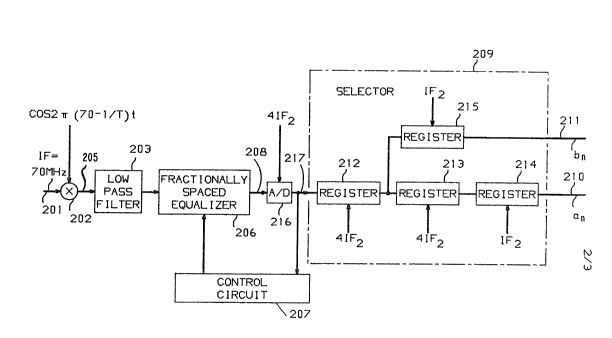
Refer now to FIG. 2. After propagating through a dispersive
transmission channel, the distorted modulated quadrature-related carrier
signals are coupled from the receiving antennas through conventional
frequency translation apparatus (both not shown). This frequency
translation apparatus in the illustrated embodiment provides a QAM signal
on lead 201 whose IF frequency is 70 M Hz. Now, pursuant to the present
invention, multiplier 202, supplied with an appropriate multiplying signal,
frequency $ranslates this 70 MHz IF frequency to provide a QAM signal on
lead 205 whose carrier frequency, designated as IF2, is an integer multiple of
the baud rate 1/T and is preferably equal to the baud rate. For this
preferred case, multiplier 202, as illustrated, is supplied with a multiplying
signal cos2~(70 - T )t.
The signal from multiplier 202 is passed through low p2SS
filter 203 to remove the harmonics introduced by frequency translation and
is then coupled through equalizer 206. Equalizer 206 is a single fractionally
spaced equalizer typically having a tapped delay line and a plurality of tap
weights which are regulated by conventional control circuit 207 so that the
distortion compensation provided varies with the distortion present in the
received QAM signal. Use of the latter eliminates the need to employ 1/2
Nyquist filters or the like in the receiver. Equalizer 206 can either be at the
input to the A/D converter, as shown, or it can be at the output of the A/D
converter, depending on whether it is to be implemented in an analog or
digital fashion, respectively. ~t this juncture, it should also be understood
that the use of multiplier 202 is not required if the IF signal created by
summing the outputs of multipliers 127 and 12~ in FIG. 1 has a frequency
30 which is an integer multiple of the baud rate and this frequency is
transmitted to the receiver. In such a case, the required mathematically
described relationship would be
~26S~
-- 5 --
fiF--m T Hz (1)
where f,F is the IF frequency in H~, m is a positive integer, and T is the
baud interval in seconds.
Assuming that equalizer 206 is a conventional, adaptive,
5 fractionally spaced equalizer whose coef~lcients are updated by control
circuit 207, it can be shown that the data signals appearing on leads 135
and 136 of FIG. 1 can be directly recovered by seiecting certain ones of the
outputs of A/D converter 216 each baud interval so long as A/D
converter 216 is clocked at a frequency which a~oids aliasing in the spectra
10 of the carrier signals on lead 208. One such clocking frequency is a~IF2, i.e.,
4 times the center frequency of the signal appearing on lead 205. Let us
assume that we would always conveniently choose the clocking frequency of
the A/D converter at the receiver to be 4IF2. Then the delay of
element 150 in FIG. 1 should be governed by:
Delay =--seconds (2)
4m
where T is again the baud interval and m is the positive integer used in
equation (1). Although other delay choices are possible under specific
conditions, the relationship expressed by equations (1) and (2) are also
appropriate. For purposes of discussion, it will hereinafter be assumed that
20 the QAM signal center frequency transmitted to the receiver = 1/T, which
means a selection of m = 1 in equations (1) and (2).
To understand how the data signals can be recovered by
selection of the certain ones of the outputs of A/D converter 216 each baud
interval, consider that an ideal IF QAM signal having a carrier frequency of
25 1/T can be represented as:
1 T
cos2~rTt ~ anp(t--nT~ ~ sin27rTt ~ bnp(t--nT--4 ); (~)
n----oo n~--oo
where an and bn are the digital
symbols embedded in the data signals on leads 135 and 136,
respectively, and the subscript n is an integer that denGtes
~%65~
-- 6 --
their position in time;
p(t) is the impulse response time function; and
T is the symbol period or baud interval.
FIG. 3 shows the waveform cos21r T t, designated as 301, and ~
5 single symbol weighted impulse time function aOp(t~, designated as 302. If
the A/I) converter 21B of FIG. 2 outputs signals every T/4 seconds and we
assume for the moment that the second term
oo T
sin2~r T t ~ bnp(t--nT--4 ~ is 0, then the output of A/D converter 21B,
n --oo
comprised of terms like the product of waveforms 301 and 302, can be
10 tabulated as a function of discrete time samples as shown in Table I.
T~BLE I
Output Time
aO OT
O T/4
aO 2T/4
0 3T/4
al T
0 11/4T
a11 1/2T
0 1 3/4T
a2 2T
o 2 1/4~
a2 21/2T
In the foregoing tabulation, aO, al, a2 represent successive digital
symbols on leads 135 and aO, al, a2 represent different combinations of the
30 transmitted aq, symbols. Accordingly, aO, al and a2 are each ~ymbol
sequence dependent and each bears no direct relationship to aO, al and a2,
~5~
-- 7 -
respectively.
Refer now to FIG. 4 which shows the function sin27r T ~
designated as 401, and a single symbol weighted impulse time function
bop(t--4 ) designated as 402, where delay element 150 of FIG. 1 has
5 provided a del~y of T/4 seconds. The product of waveforms like 401 and
402, exemplifying part of the sampled output of A/D converter 21~, can be
tabulated as shown in Table II.
TABLE II
Output Time
o OT
bo T/4
O ~/2
bo 3T/4
O T
bl1 1/4T
0 1 1/2T
bl1 3/4T
0 2T
b22 1/4T
In Table II, symbols bo~ bl, etc., represent successive digital
25 symbols on lead 13~ and symbols bo~ b1, etc., represent different
combinations of the transmitted bn symbols and are, therelore, symbol
sequence dependent. Consequently, bo and b1 each have no direct
relationship to bo and b1, respectively.
An examination of Tables I and II reveals that at the output of
30 A/D conve~ter 216, the symbols an and bn each appear explicitly at
different times and that the appearance of any an symbol in Table I is
concurrent with the appearance of a zero sample in Table II. Likewise, the
appearance of any bn symbol in Table II is concurrent with the appearance
~2652~
of a zero sample in Table I. Hence, with a delay of T/4 provided by delay
element 150 of FIG. 1, the initial assumption that the term
t ~r
sin27r T ~ bnp(t--nT-- 1 ) = O in forming Table I is not required and
n --oo 4
the results of Tables I and II can be superimposed in accordance with
5 equation (3) to yield Table III.
TABLE III
Output of A/D Converter 216 Time
a~ OT
bo T/4
10 aO T/2
bo 3T/4
al T
bl ST/4
al 6T/4
15 b l 7T/4
a2 2T
b2 2 1/4T
Table m clearly shows that 2 of the 4 outputs provided by A/D
converter 216 each symbol period are the digital symbols on leads 135 and
136. Speci~lcally, symbols aO, al, a2,..., which are the signals on lead 135 in
FIG. 1, appear at times t=OT, T, 2T,... and symbols bo~ bl, b2,..., which are
the signals on lead 136 in FIG. 1, appear at times t=T/4, 1 1/4T, 21/4T,
etc.
Now, refer back to FI(~. 2. The output of equalizer 206is
connected to A/D converter 216 which, clocked at 4IF2, quantizes the
analog QAM signal into a preselected number of digital signal levels. The
number of these digital signal levels is at least equal to those provided by
D/A converters 122 and 123 in FIG. 1. These signal levels appear on
bus 217 and are supplied to selector 20~.
Selector 209 is connected to bus 217 and respectively couples the
transmitted digital symbols designated as an and bn to buses 210 and 211.
These di~ital symbols are coupled to baseband receiver circuitry for further
signal processing. Control circuit 207 which adjusts the distortion
Z~32
compensation provided by equalizer 206 acts in conventional f~hion to the
outputs of A/D converter 216 appearing on bus 217.
Selector 20~ comprises three serially connected, parallel-in,
parallel-out registers 212, 213, 214 and a parallel-in, parallel-out register 215
5 connected to the output of register 212. To selectively couple only digital
symbols an and bn to buses 210 and 211, registers 212 and 213 are clocked
at 4IF2 and registers 214 and 215 are clocked at IF2. Each register provides
a delay equal to one period of its associated clocking signal.
It should, of course, be understood that while the present
10 invention has been disclosed in terms of a specific embodiment, numerous
other arrangements may be apparent to those sl~illed in the art without
departing from the spirit and scope of the invention. For example, if
equalizer 206 was digitally implemented, then A/D converter 216 would
immediately precede it and the outputs of equalizer 206 would be coupled to
15 selector 209 and control circuit 207.